Intel Labs Petersburg: Oleg Semenov about SoC, programmable accelerators and new algorithms
Habra Yesterday I touched on the subject of Intel laboratories, but very superficially. Today - an interview with one of the leaders of such a laboratory, and all this within the framework of the program " 5 weeks with Intel ".
Intel Labs is a research division of Intel, with offices in 11 countries and engaged in various innovative developments for the benefit of the company. Read more about Intel Labs in an interview with Jerry Baptiste, Chief Business Development Manager at Intel Labs; As of 2009, Intel Labs Europe includes about 900 scientists in 20 laboratories.
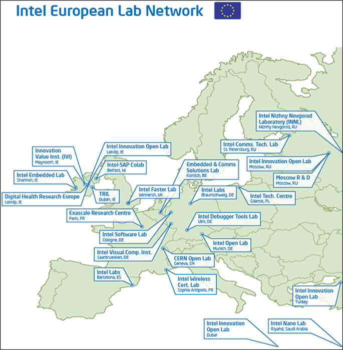
The Intel Labs Europe map, which shows not only the offices of Intel Labs, but also the laboratories of the organization Intel Labs Europe, belonging to other business groups of Intel.
In Russia, too, there is Intel Labs, it is part of the St. Petersburg office of the corporation and is now engaged in systems-on-chip, the creation of programmable accelerators and signal processing algorithms for mobile platforms. One of the successful projects of the laboratory was the development of wireless video transmission technology, which can be used to transmit video from mobile devices and laptops to televisions and plasma panels. The laboratory took part in the development and research of many wireless and wired standards (Wi-Fi, Wi-Max, UWB, WUSB, 10 Gbit Ethernet), dealt with the problems of "cognitive" radio in part of the study of effective programmable architectures for the integration of various wireless technologies in one chip .
')
The activities of the laboratory established in Nizhny Novgorod and eventually moving to St. Petersburg are supervised by Oleg Semenov. During its work, the laboratory issued more than 65 patents, and the number of filed applications for inventions has long exceeded 200.
Oleg agreed to talk about the activities of the St. Petersburg office of Intel Labs and show the development of his team, which already has about 30 people.

Tell about yourself and your work?
My main area of interest is DSP, digital signal processing. Since the early nineties, I headed the laboratory of digital signal processing at the State University of Telecommunications. Bonch-Bruevich, where we worked on various projects, one way or another related to DSP: speech processing, effective transmission of information through telephone lines, radio channels, and so on. At the end of 2002, Intel opened a telecommunications development lab in Nizhny Novgorod (at that time, Intel had an R & D site only in Nizhny Novgorod); My colleague Vladimir Ivanov and I were invited to head it, so in February 2003 we formed this laboratory from scratch.
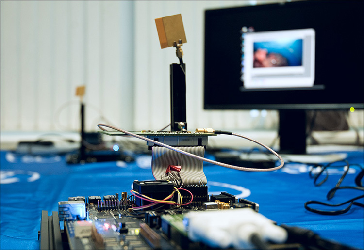
Intel Wireless Display Prototype The module and antenna transmitter are visible; the background is a signal receiver connected to the monitor. A distinctive feature of the prototype is a small delay (only a few milliseconds - significantly less than the Wi-Di product announced at the beginning of this year), which allows not only transmitting a video image, but even playing some 3D shooters.
It is noticeable that in the demo office of Intel Labs in St. Petersburg, DSP, digital signal processing runs the red thread.
Yes, without digital processing, nowhere is video processing and 3D processing, so it is not surprising that DSP underlies the activities of many of our groups within the laboratory. In addition, St. Petersburg is famous for the fact that there are a lot of specialists in the field of telecommunications and signal processing, so the relocation of the laboratory to St. Petersburg was also quite logical. It was also due to close contacts with some St. Petersburg universities, the technical and scientific expertise of which was in the interests of Intel.
What are the main areas of the St. Petersburg laboratory?
There are three of them: 1) development of system-on-chip design tools (SoC, system-on-chip), 2) development of architectures for programmable accelerators and 3) development of new algorithms for these accelerators. I will tell you more about each of our destinations.
The relevance of developing system-on-chip design methodologies is increasing every day, since the number of transistors on a chip is increasing at a tremendous pace and the cost of developing such systems is increasing very much.
Do you mean the tools for designing and modeling systems on a chip?
Yes, now this is a whole direction: modeling tools, design and programming of such systems. The degree of programmability of the components and units that make up the SoC, system-on-chip, may differ from the classical general purpose CPU (universal microprocessors) and classical DSP chips (digital signal processing units). In universal CPUs and DSP chips, the degree of programmability can be quite wide, but you have to pay for this with higher power consumption, lower performance, and larger chip area. As a result, a universal silicon solution may be less effective compared to a non-programmable “iron” solution that is focused on the solution of a concatenation problem (such non-programmable solution is called ASIC, Application Specific Integrated Circiut). But ASIC cannot be used for other applications. Therefore, the task of building an intermediate solution, which has limited programming capabilities (for example, is focused on applications of a particular class), but at the same time having performance indicators much better than a CPU or DSP and solving problems from the same class of applications, is a pressing problem today. features - for modern mobile platforms. The use of programmable accelerators oriented to different classes of applications is presented as a reasonable way to increase the efficiency of devices based on SoC solutions. Obviously, system-on-chip development methods are extremely important especially for the mobile platform and embedded systems markets, so Intel pays serious attention to these highly competitive markets to grow their business. But to be a leader in this market, it is necessary to develop effective methods for developing systems on a chip, which we are doing.
As I have already mentioned, we are also engaged in effective architectures of programmable accelerators, accelerators, and tools for their design and programming. One of the demonstrations you saw relates to building efficient accelerator structures that can be programmable, but not universal.
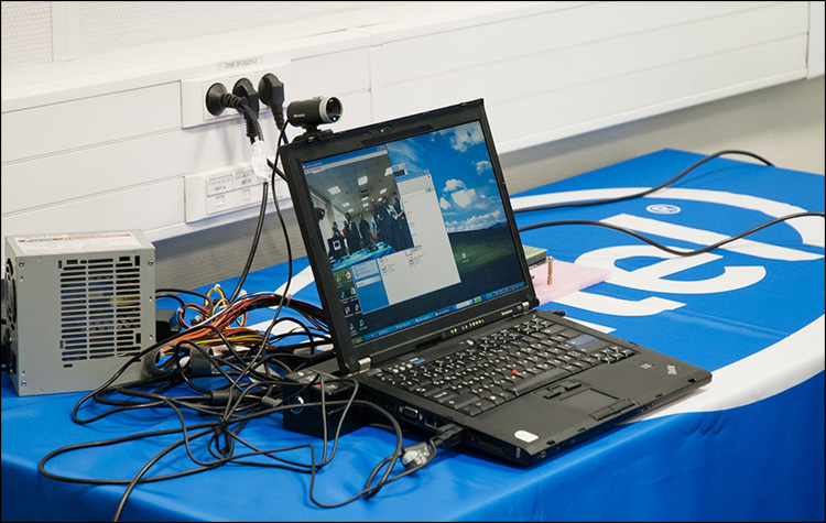
A video camera is connected to the laptop, recognizing objects (for example, a logo drawn on paper) using a specialized accelerator. It doesn’t look too impressive, but the future of mobile platforms stands behind energy-efficient specialized accelerators.
A demo that recognizes the image - it can be developed in some mobile devices that will allow you to do pattern recognition or perform augmented reality applications?
Of course. Actually, it was for these purposes that this project was put. It is necessary to create design tools for such an accelerator, and for this purpose an approach called workload-driven design is used. Let me explain: you have an application that you want to speed up hardware in the future, and the chip designer, who will speed up this application, needs some tool that will help this designer, given this application, design the architecture of the future accelerator. If the design of such a chip is done manually, then it will take you a lot of time, and the effectiveness of this solution may be worse than using special development tools.
There is a direction that is called high-level synthesis, that is, high-level synthesis, when you go from the application and go down in the design process in order to obtain an efficient architecture of the future chip, aimed at this application. At the same time there are special tools that allow you to do this in the most efficient way. This does not mean that such tools will work at the touch of a single button. Of course, the designer’s active involvement in the chip development process is relied upon, but the main benefit of such a development tool is that you can evaluate the quality of the future crystal in terms of area and energy efficiency at an early design stage, without bringing the design to real silicon baking and, accordingly by avoiding huge production losses.
Again, at an early stage of development, you can test the future chip as much as possible, since it is no secret that there are always errors that it is better not to bring to real silicon, and to solve which costs a higher level. There is a so-called RTL level, register transfer level - this is when you present your microcircuit, which will be baked in silicon in the future, in the form of a certain description in a more or less high-level language called HDL (hardware description language - the most popular representatives of HDL Verilog and VHDL). Then you lower the RTL to real transistors, a logic level, and so on. There, the level of abstraction is significantly lower, and it is difficult to find design errors. If you can carry out the verification process of your future crystal at earlier design stages and remove the maximum number of errors that occur, then this will allow you to significantly reduce the cost of the chip and reduce the time it takes for the device to enter the market (time to market) and, naturally, be ahead in a tough competitive environment.
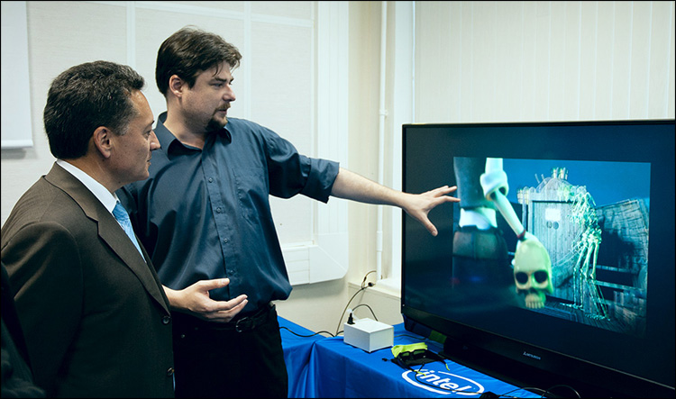
An employee of the laboratory demonstrates Intel's CEO in Europe, the Middle East and Asia, Christian Morales, a technology for creating a signal depth map based on a two-dimensional image. A three-dimensional image that requires special glasses is obtained using an ingenious algorithm that processes a completely ordinary Bluray film shot without the use of a stereo camera. This technology will soon appear on the market and allow you to view movies shot in the usual way, in a very convincing 3D.
That is, it is hoped that in the foreseeable future there will be small teams that can quickly and cheaply design some specialized solutions based on such tools?
Exactly. And our developments are aimed at improving the competitiveness of the company in the field of SoC design, primarily in terms of time to market, that is, in time to bring these solutions to the market, because the SoC market itself is very diversified and dynamic.
We are engaged in accelerator architectures, tools for their development, and it is quite natural that we are also engaged in new algorithms. Why? Because, as I said, the accelerators themselves must be workload-driven, that is, determined primarily by the tasks performed, so we need to keep abreast of modern algorithms, to understand what computational procedures are used in modern applications. Knowledge of applications, their deep understanding is very important in order to build an effective accelerator architecture and tools for designing these accelerators.
It turns out that these are some such Eulerian circles of related topics that in the St. Petersburg laboratory rather strongly overlap each other?
Right. If earlier there was a clear division into algorithmic engineers, programmers and hardware engineers who made the crystal, and it was difficult to find a person who would cover all three parts of the task. Now there is a process of convergence of these themes in some kind of universal chip designer, who dances from the application and which, in principle, at least at the first stage of design, may not be a strong connoisseur of the hardware. Development tools should allow him to implement the chip design, without being strongly aware of the details of the hardware design, that is, significantly increase the level of design abstractions of the chip. Further, when the designer reaches the RTL level mentioned above, the register transfer level, standard tools from different companies that already exist on the market, such as Synopsys and Cadence, can be used to bring the design to real silicon. But the process of high-level design today has the greatest complexity. Chip designers spend a lot of time on it, and it is there that it is important to get a time gain in terms of time to market.
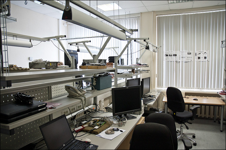
One of the premises of Intel Labs in St. Petersburg.
Do you work with universities and external teams?
We are actively working with Russian universities and pay great attention to this. Within our projects, university staff and scientists defended several dozen patents, including those for Intel. For example, we consider our partners in the University of Aerospace Instrumentation as a kind of lablet - a laboratory inside our laboratory. Formally, these are not our employees, but, nevertheless, we regard them as a serious potential for the growth of our scientific baggage, and attract them to solve rather complex problems. The resource that we have at the university seriously expands our possibilities in the field of researching those things that we simply could not reach. In addition, we try to work with universities where there are world-class experts, since Intel is only interested in the highest-class projects. Fortunately, such potential has remained at Russian universities, and it’s great that we manage to find common points of contact and common points of interest. We continue to expand our cooperation with Russian universities.
To be continued!
Intel Labs is a research division of Intel, with offices in 11 countries and engaged in various innovative developments for the benefit of the company. Read more about Intel Labs in an interview with Jerry Baptiste, Chief Business Development Manager at Intel Labs; As of 2009, Intel Labs Europe includes about 900 scientists in 20 laboratories.
The Intel Labs Europe map, which shows not only the offices of Intel Labs, but also the laboratories of the organization Intel Labs Europe, belonging to other business groups of Intel.
In Russia, too, there is Intel Labs, it is part of the St. Petersburg office of the corporation and is now engaged in systems-on-chip, the creation of programmable accelerators and signal processing algorithms for mobile platforms. One of the successful projects of the laboratory was the development of wireless video transmission technology, which can be used to transmit video from mobile devices and laptops to televisions and plasma panels. The laboratory took part in the development and research of many wireless and wired standards (Wi-Fi, Wi-Max, UWB, WUSB, 10 Gbit Ethernet), dealt with the problems of "cognitive" radio in part of the study of effective programmable architectures for the integration of various wireless technologies in one chip .
')
The activities of the laboratory established in Nizhny Novgorod and eventually moving to St. Petersburg are supervised by Oleg Semenov. During its work, the laboratory issued more than 65 patents, and the number of filed applications for inventions has long exceeded 200.
Oleg agreed to talk about the activities of the St. Petersburg office of Intel Labs and show the development of his team, which already has about 30 people.
Tell about yourself and your work?
My main area of interest is DSP, digital signal processing. Since the early nineties, I headed the laboratory of digital signal processing at the State University of Telecommunications. Bonch-Bruevich, where we worked on various projects, one way or another related to DSP: speech processing, effective transmission of information through telephone lines, radio channels, and so on. At the end of 2002, Intel opened a telecommunications development lab in Nizhny Novgorod (at that time, Intel had an R & D site only in Nizhny Novgorod); My colleague Vladimir Ivanov and I were invited to head it, so in February 2003 we formed this laboratory from scratch.
Intel Wireless Display Prototype The module and antenna transmitter are visible; the background is a signal receiver connected to the monitor. A distinctive feature of the prototype is a small delay (only a few milliseconds - significantly less than the Wi-Di product announced at the beginning of this year), which allows not only transmitting a video image, but even playing some 3D shooters.
It is noticeable that in the demo office of Intel Labs in St. Petersburg, DSP, digital signal processing runs the red thread.
Yes, without digital processing, nowhere is video processing and 3D processing, so it is not surprising that DSP underlies the activities of many of our groups within the laboratory. In addition, St. Petersburg is famous for the fact that there are a lot of specialists in the field of telecommunications and signal processing, so the relocation of the laboratory to St. Petersburg was also quite logical. It was also due to close contacts with some St. Petersburg universities, the technical and scientific expertise of which was in the interests of Intel.
What are the main areas of the St. Petersburg laboratory?
There are three of them: 1) development of system-on-chip design tools (SoC, system-on-chip), 2) development of architectures for programmable accelerators and 3) development of new algorithms for these accelerators. I will tell you more about each of our destinations.
The relevance of developing system-on-chip design methodologies is increasing every day, since the number of transistors on a chip is increasing at a tremendous pace and the cost of developing such systems is increasing very much.
Do you mean the tools for designing and modeling systems on a chip?
Yes, now this is a whole direction: modeling tools, design and programming of such systems. The degree of programmability of the components and units that make up the SoC, system-on-chip, may differ from the classical general purpose CPU (universal microprocessors) and classical DSP chips (digital signal processing units). In universal CPUs and DSP chips, the degree of programmability can be quite wide, but you have to pay for this with higher power consumption, lower performance, and larger chip area. As a result, a universal silicon solution may be less effective compared to a non-programmable “iron” solution that is focused on the solution of a concatenation problem (such non-programmable solution is called ASIC, Application Specific Integrated Circiut). But ASIC cannot be used for other applications. Therefore, the task of building an intermediate solution, which has limited programming capabilities (for example, is focused on applications of a particular class), but at the same time having performance indicators much better than a CPU or DSP and solving problems from the same class of applications, is a pressing problem today. features - for modern mobile platforms. The use of programmable accelerators oriented to different classes of applications is presented as a reasonable way to increase the efficiency of devices based on SoC solutions. Obviously, system-on-chip development methods are extremely important especially for the mobile platform and embedded systems markets, so Intel pays serious attention to these highly competitive markets to grow their business. But to be a leader in this market, it is necessary to develop effective methods for developing systems on a chip, which we are doing.
As I have already mentioned, we are also engaged in effective architectures of programmable accelerators, accelerators, and tools for their design and programming. One of the demonstrations you saw relates to building efficient accelerator structures that can be programmable, but not universal.
A video camera is connected to the laptop, recognizing objects (for example, a logo drawn on paper) using a specialized accelerator. It doesn’t look too impressive, but the future of mobile platforms stands behind energy-efficient specialized accelerators.
A demo that recognizes the image - it can be developed in some mobile devices that will allow you to do pattern recognition or perform augmented reality applications?
Of course. Actually, it was for these purposes that this project was put. It is necessary to create design tools for such an accelerator, and for this purpose an approach called workload-driven design is used. Let me explain: you have an application that you want to speed up hardware in the future, and the chip designer, who will speed up this application, needs some tool that will help this designer, given this application, design the architecture of the future accelerator. If the design of such a chip is done manually, then it will take you a lot of time, and the effectiveness of this solution may be worse than using special development tools.
There is a direction that is called high-level synthesis, that is, high-level synthesis, when you go from the application and go down in the design process in order to obtain an efficient architecture of the future chip, aimed at this application. At the same time there are special tools that allow you to do this in the most efficient way. This does not mean that such tools will work at the touch of a single button. Of course, the designer’s active involvement in the chip development process is relied upon, but the main benefit of such a development tool is that you can evaluate the quality of the future crystal in terms of area and energy efficiency at an early design stage, without bringing the design to real silicon baking and, accordingly by avoiding huge production losses.
Again, at an early stage of development, you can test the future chip as much as possible, since it is no secret that there are always errors that it is better not to bring to real silicon, and to solve which costs a higher level. There is a so-called RTL level, register transfer level - this is when you present your microcircuit, which will be baked in silicon in the future, in the form of a certain description in a more or less high-level language called HDL (hardware description language - the most popular representatives of HDL Verilog and VHDL). Then you lower the RTL to real transistors, a logic level, and so on. There, the level of abstraction is significantly lower, and it is difficult to find design errors. If you can carry out the verification process of your future crystal at earlier design stages and remove the maximum number of errors that occur, then this will allow you to significantly reduce the cost of the chip and reduce the time it takes for the device to enter the market (time to market) and, naturally, be ahead in a tough competitive environment.
An employee of the laboratory demonstrates Intel's CEO in Europe, the Middle East and Asia, Christian Morales, a technology for creating a signal depth map based on a two-dimensional image. A three-dimensional image that requires special glasses is obtained using an ingenious algorithm that processes a completely ordinary Bluray film shot without the use of a stereo camera. This technology will soon appear on the market and allow you to view movies shot in the usual way, in a very convincing 3D.
That is, it is hoped that in the foreseeable future there will be small teams that can quickly and cheaply design some specialized solutions based on such tools?
Exactly. And our developments are aimed at improving the competitiveness of the company in the field of SoC design, primarily in terms of time to market, that is, in time to bring these solutions to the market, because the SoC market itself is very diversified and dynamic.
We are engaged in accelerator architectures, tools for their development, and it is quite natural that we are also engaged in new algorithms. Why? Because, as I said, the accelerators themselves must be workload-driven, that is, determined primarily by the tasks performed, so we need to keep abreast of modern algorithms, to understand what computational procedures are used in modern applications. Knowledge of applications, their deep understanding is very important in order to build an effective accelerator architecture and tools for designing these accelerators.
It turns out that these are some such Eulerian circles of related topics that in the St. Petersburg laboratory rather strongly overlap each other?
Right. If earlier there was a clear division into algorithmic engineers, programmers and hardware engineers who made the crystal, and it was difficult to find a person who would cover all three parts of the task. Now there is a process of convergence of these themes in some kind of universal chip designer, who dances from the application and which, in principle, at least at the first stage of design, may not be a strong connoisseur of the hardware. Development tools should allow him to implement the chip design, without being strongly aware of the details of the hardware design, that is, significantly increase the level of design abstractions of the chip. Further, when the designer reaches the RTL level mentioned above, the register transfer level, standard tools from different companies that already exist on the market, such as Synopsys and Cadence, can be used to bring the design to real silicon. But the process of high-level design today has the greatest complexity. Chip designers spend a lot of time on it, and it is there that it is important to get a time gain in terms of time to market.
One of the premises of Intel Labs in St. Petersburg.
Do you work with universities and external teams?
We are actively working with Russian universities and pay great attention to this. Within our projects, university staff and scientists defended several dozen patents, including those for Intel. For example, we consider our partners in the University of Aerospace Instrumentation as a kind of lablet - a laboratory inside our laboratory. Formally, these are not our employees, but, nevertheless, we regard them as a serious potential for the growth of our scientific baggage, and attract them to solve rather complex problems. The resource that we have at the university seriously expands our possibilities in the field of researching those things that we simply could not reach. In addition, we try to work with universities where there are world-class experts, since Intel is only interested in the highest-class projects. Fortunately, such potential has remained at Russian universities, and it’s great that we manage to find common points of contact and common points of interest. We continue to expand our cooperation with Russian universities.
Let me remind you that this post was written as part of the " 5 weeks with Intel " program - we chose 5 interesting topics and every week we will post one interview with one of the company's executives. All registered users will be able to ask questions under the topic, and a little later - to receive a response directly from the employee of the company. The most interesting questions we will encourage prizes;) By the way, last week, dedicated to the MeeGo operating system , the “winner” was the user of Labinskiy , with which we congratulate him. By the way, last week, dedicated to the MeeGo operating system , the “winner” was the user of Labinskiy , with which we congratulate him.And yet - do not forget to connect to the company's blog on the site! |
Source: https://habr.com/ru/post/97350/
All Articles