DIY debug board for Atmega32
1. Introduction
After reading a lot of posts and comments from DIY, it seemed to me that there are a lot of people here who are interested in microcontrollers and their programming. Even more people who would like to start, but do not know where.
I think that you need to start with the practice, because I will not consider emulators.
First you need a programmer, but there are tons of information about this on the Internet, so I’ll stop only superficially. The easiest of them is the so-called "5 wires", to make it easy - take the LPT cable and connect it to the MK via resistors, as shown in the figure:
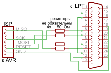
It is necessary to do everything with the utmost care, to burn the LPT like this - at times.
It is much better to do something more decent - for example, USBasp is safer and works via USB.
As an option - buy a programmer in the same Voltmaster or Chip-and-Dip.
The parameters are not so important for the beginning, except for the price and supported chips.
')
Essentially everything. Crystal + programmer + desire and desire, this is enough to do programming MK. But still very important is the organization of the circuit itself and the periphery (strapping) of the IC.
Of course, you can make a printed circuit board for every occasion when you want to play, but I am for more versatile and fast solutions.
Of course, there are prototypes, but for me, the web of wires and jumpers looks awful, and unreliable and, most importantly, not intuitive (and this is important when developing and training).
There are debug boards for various microcontrollers. And everything in them is good, except for the price (the simplest of 2-3 thousand rubles - it is certainly worth it, but then it is amateur radio, so that if possible you can do it yourself). So I decided to create my own simple debugging board that will meet my requirements.
What are the requirements for this board:
- Ease of execution
- Visibility
- Versatility
- Cheapness
- Easy to create test device
- LCD display
- Built-in keyboard
- 2 free ports (with the option to use them at your discretion)
- COM port at the board for computer integration
What was used in the manufacture of:
- One-side glass fiber laminate ~ 70p
- Pads for connecting peripherals and switching (pins as on motherboards, on which jumpers are hung) ~ 50p
- Clock buttons - ~ 50p
- Socket for chip 30p
- Connector for COM port 20p
- Chip MAX232a 50r
- LCD indicator - from 250r
- The ATmega32 chip from 200r
total 720p at Moscow crazy prices for radio components (or rather, the price of Voltmaster).
that's what I ended up with:

2. Wiring
Now in order. Let's start with the layout of the board in Sprint-Layout. In fact, this is the most crucial moment in the creation of the device, you need to take into account all the nuances, and at this point you need to understand what exactly is required of the board, how it should look, how more convenient. Therefore, I do not advise you to repeat blindly, it is worth sitting down and looking at analogs, isolating interesting solutions or nodes for yourself. I did it like this:

More about the periphery, for this you should look at the pinout of the crystal:

- The keyboard will hang on the PORTA - 7 buttons arranged so that they can be used to navigate, if necessary, for example, through the menu (cross), and a pair of buttons for additional functions.
- on PORTB, I placed the LCD display, in a way that is provided for in codevision avr by standard means (three command display registers and 4 data registers are used)
- PORTC and PORTD brought pads for connecting peripherals. I also provided collet panels next to the pads, but in my household they didn’t turn out and their installation was postponed until better times
- I also placed the max232 with a capacitor strapping and a COM port connector.
more about connecting max232 - For versatility, each pin of the controller is displayed on the pads parallel to the socket for the chip.
- The programming pins SCK, MISO, MOSI and RESET are duplicated by another row of pads
3. Making signets
As soon as the board was diluted, a signet was made using a laser-iron method. it makes no sense to dwell on the method, as it has been described on the Internet hundreds of times, and at least a detailed description is on Habré . Result:

4. The final stage
further we drill, we puddle, we solder our board.

5. Conclusion
And so, our debug board to simplify development on the MK is ready. Now, in order to learn how to work with the AVR MK functionality, we will not have to sculpt a tangle of wires. we simply connect the necessary peripherals to the free ports (be it LEDs, sensors, drivers, drives and servos, as well as many other things), and calmly write the program.
In conclusion, I want to say that the type and functionality of this board was formed on the subjective requirements and desires, and everyone who wants to make such a device should sit down and think about the formulation of the problem and requirements.
All the work went one evening.
Article written by nortonix .
Source: https://habr.com/ru/post/93099/
All Articles