5 nm vs 3 nm
Intermediate manufacturing processes, different types of transistors, and many other options add uncertainty to the electronics manufacturing process.
Electronics manufacturers are gearing up for the next wave of cutting-edge manufacturing processes, but their customers will be confused with a bunch of confusing options - whether to develop chips using the 5 nm process technology, wait 3 nm, or choose something in between.
The path to 5 nm is well defined, unlike 3 nm. After that, the landscape becomes confused as factories add intermediate manufacturing processes, such as 6 nm and 4 nm. Switching to any of these technical processes is very expensive, and the benefits are not always obvious.
Another cause for concern is the shrinking manufacturing base. In the case of the most advanced technical processes, the choice of manufacturers is small. There were several leading manufacturers in the industry, but over time this area has narrowed due to a sharp increase in cost and a decrease in the user base. In general, the fewer manufacturers, the fewer options for technology and price tag.
Today, Samsung and TSMC are the only two manufacturers working with technological processes of 7 nm or lower, although this may change. Intel and the Chinese company SMIC are developing advanced manufacturing processes. Intel, not the largest player in the field of commercial production, is experiencing problems with the development of the 10 nm process technology. And it is unclear whether SMIC will be able to give out 7 nm, since this topic is still in the research and development stage (the same thing happens with Intel with the 10 nm process technology).
')
As for more advanced manufacturing processes, Samsung and TSMC work with 7 nm using finFET transistors, and both manufacturers are going to continue this at 5 nm. Unlike traditional planar transistors, finFETs are three-dimensional structures with better performance and less leakage.
Then at 3 nm Samsung will move from finFET to the new nanosheet FET transistor architecture, which is a development of finFET technology. TSMC has not yet revealed its plans for 3 nm, leaving many customers in limbo. TSMC, according to sources, weighs a variety of options, including nanolayers, nanowires and forced finFETs. Intel, TSMC, and others are also working on new forms of advanced packaging as possible options for downscaling.
However, at 3 nm the size of transistor technology can go in different directions. finFET can still play, but this technology needs some breakthroughs. Apparently, the industry will have to prepare for the transition to the new architecture of the 3 nm process technology, and the next intermediate process process at 2 nm, judging by the development plans of one organization working in this area.
“5 nm is still finFET,” said Naoto Horiguchi, program director at Imec. - Let's say that at 3 nm we will enter a transition period from finFET to other architectures. We believe that these will be nanolayers. ”
Nanolayer FETs relate to the architecture of gate-all-around transistors (GAA). And this is not the only option. “The industry is very conservative. Its participants will try to squeeze everything from finFET to the limit, ”said Horiguchi. - At the 3 nm manufacturing process, we have the opportunity to use finFET. But we will need to make a few finFET innovations, to improve it in general. ”
Will chip manufacturers stay on the 7 nm process technology, migrate to 5 nm, 3 nm or to the intermediate? 7 nm provides enough performance for almost all applications, so this process will live for a long time. Outside there are several high-performance options, and they all cost more. And we will see if these technologies have time to appear on time.
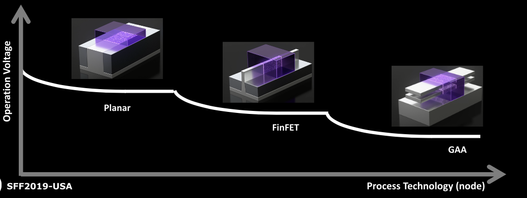
The operating voltage of various manufacturing processes is planar transistors, finFET and nanolayer FET.
Ruin of production
The chip consists of many transistors acting as switches. For many decades, the progress of integrated circuits was in accordance with Moore's law, according to which the density of transistors on a device doubles in a period of 18 to 24 months.
In a similar rhythm, manufacturers introduced new technological processes with a higher density of transistors, which allowed the industry to reduce the cost of chips in terms of the number of transistors. At each manufacturing process, manufacturers scaled transistor specifications 0.7 times, allowing the industry to increase productivity by 40% with the same energy consumption and a two-fold reduction in area.
The integrated circuit industry followed this formula and flourished. Since the 1980s, it has paved the way for fast PCs at discounted prices.
By 2001, there were already at least 18 manufacturers with factories where they could manufacture chips at 130 nm, which at that time was an advanced technical process, according to IBS. Also then, several more new manufacturers appeared, making custom-made chips at other people's factories. In addition, chip manufacturing was practiced for laboratories that developed them, but did not have their own production.
By the end of the decade, the cost of production and manufacturing processes surged. Unable to cope with the price increase, many chip manufacturers switched to the fab lite model. They produced some chips at home, and the rest were outsourced.
Over time, fewer chip manufacturers made advanced devices at their own facilities. Some completely got rid of production or left this business.
However, in the 2000s, a business model of silicon workshops appeared. Workshops lagged behind Intel and other technology companies, but gave design companies access to various processes.
The next major change occurred at the 20 nm stage, when traditional planar transistors hit a wall and encountered a short channel effect . In response, Intel switched to next-generation transistor technology, finFET, at 22 nm in 2011. Workshops switched to finFET at 16/14 nm.
FinFET has several advantages over planar transistors. “In this scheme, the entire transistor extends vertically so that the channel rises above the substrate, and the valve wraps around three sides of the fin. The increased contact area of the valve allows better control of the leakage current, ”write Matt Kogorno and Toshihiko Miyashita from Applied Materials. Kogorno is the director of global product management, and Miyashita is the chief technologist.
FinFET is also more complex devices, it is more difficult to produce and scale them for each next technological process. As a result, the cost of R&D rose to heaven. So now the rhythm of a full-fledged process change has grown from 18 months to 2.5 years or more.
Integrated circuit prices also continue to rise. The cost of developing a planar device at 28 nm varies from $ 10 million to $ 35 million, according to Gartner. For comparison, the cost of designing a single-chip system (SoC) at 7 nm varies from $ 120 million to $ 420 million.
“The development cost is highly dependent on SoC complexity,” said Samuel Wen, an analyst at Gartner. - Two-thirds go to the development of the chip. The rest is the development of submarines, the cost of masks and improved output. Over time, the cost of design also falls. ”
However, price trends have changed the landscape of the world of integrated circuits. Over time, fewer companies can afford to pay for chip design for the most advanced manufacturing processes. Many of them rely on workshops for production issues.
A decrease in the number of customers along with an increase in the cost of production influenced the landscape of workshops producing advanced chips. For example, there are five manufacturers / workshops left on the 16/14 nm market: GlobalFoundries, Intel, Samsung, TSMC and UMC. SMIC also works with finFET on a 14 nm process technology.
And at 7 nm another transition occurred. Technological processes and the cost of production continued to grow, and the return on investment was already in question. As a result, GlobalFoundries and UMC last year stopped trying to develop a 7 nm process technology. Both companies continue to operate in the 16/14 nm market.
Trying to develop further, Samsung and TSMC rush at full speed to the turn of 7 nm and beyond. After several delays, Intel plans to launch production at 10 nm in mid-2019, and at 7 gm - by 2021. SMIC, meanwhile, does not promise any deadlines.
But not all workshop customers require advanced manufacturing processes. There is a thriving market for 28 nm chips. “It all depends on the characteristics of the product,” said Ven of Gartner. - Some products require maximum performance. Developers can still use outdated technical processes. And chips for applications that do not require high performance can live on the N-1 and N-2 manufacturing processes. ”
Others echo him. “How many companies can afford the latest silicon today from an economic point of view? Their number is decreasing. In markets requiring extremely high performance, such a need will always be. But in the supply chain, in terms of volumes, a fault forms in the middle. The most demanding customers require technological processes at 7, 5, and possibly someday 3 nm. But everyone else slowed down a bit, ”said Walter Eun, vice president of business management at UMC.
But in certain cases, there is a need for the most advanced chips - these are servers and smartphones. There is also a sea of new startups related to AI chips. Many companies design chips for machine learning and deep learning.
“Nobody argues that the need to count something 10 times faster than today will always be commercially useful and competitive, even in non-technical markets. All these unique achievements of deep learning technology are evidence of this. There is literally no end to the demand for ever-increasing computer power, ”said Aki Fujimura, director of D2S.
“Demands for computing power have experienced several major shifts - at first it was the GPU, and later - deep learning,” Fujimura said. - Deep learning is a massive technology for finding suitable patterns, and training neural networks is the task of consistent optimization. Now that the world has come up with a mechanism for processing a huge amount of data and turning it into useful information in the form of a program capable of logical conclusions, the number of necessary calculations grows with the amount of data available. And since the amount of data in all areas is growing exponentially, the requirements for computing power are guaranteed to grow significantly, at least in the field of deep learning. ”
Whether the AI chips require technical processes of 5 nm or more remains unclear, but there are definitely requirements for an increase in computing power. But migration to these technical processes does not become an easier or cheaper process.
5 nm vs 3 nm
Meanwhile, at the beginning of 2018, TSMC reached another milestone, becoming the first manufacturer in the world to use the 7 nm process technology. Samsung later joined the 7 nm race. The process of manufacturing chips at 7 nm is mainly based on finFET, and consists of manufacturing chips with a gate step of 56 to 57 nm and a minimum step of placing metal conductors [metal pitch] at 40 nm, according to information from IC Knowledge and TEL.
In the first version of 7 nm, TSMC used 193 nm immersion lithography and multiple patterning. This year TSMC promises to release a new version of 7 nm using extreme ultraviolet lithography (EUV). EUV simplifies the steps of the process, but it is an expensive technology and it has its own set of difficulties.
TSMC is preparing its new 5 nm process technology for release in the first half of 2020. New technology from TSMC at 5 nm will be 15% faster than 7 nm, and consume 30% less energy. The second version of the 5 nm process technology, coming out next year, will be 7% faster. Both versions will use EUV.
TSMC is already gaining orders at 5 nm. “Big orders are expected from Apple, HiSilicon and Qualcomm,” said Handel Jones, IBS Director. “The volume of substrates will be between 40,000 and 60,000 per month by the fourth quarter of 2020.”
The transition speed at 5 nm for TSMC is less than 7 nm. Firstly, 5nm is a completely new process, with updated EDA tools and patents. In addition, it is more expensive. On average, the cost of developing a device at 5 nm varies from $ 210 million to $ 680 million, according to Gartner.
Some chip makers want to get away from 7nm without spending as much money as 5nm. Therefore, TSMC recently introduced a new 6 nm process technology, cheaper, but with a few compromises.
“The numbers N6 and N5 do not seem to be different, but in fact the gap is large,” said S. S. Wei, director of TSMC at the last meeting. - At N5, in comparison with N7, the logical density is increased by 80%. N6 compared to N7 only 18%. As you can see, there is a big difference between the logical density and the efficiency of transistors. As a result, the overall power consumption of the N5 chip is lower. Switching to N5 has many advantages. But N5 is a full-fledged technical process, and it takes time for customers to develop new products for it. The beauty of N6 is that if they already have a project under N7, then they will have to spend very little effort. They can upgrade to N6 and get certain benefits. And depending on the characteristics of the product and the market, customers will decide what to do. ”
Meanwhile, Samsung rolled out 5 nm, which will appear in the first half of 2020. Compared to 7 nm, Samsung’s new 5 nm process technology at finFET provides up to 25% logic compaction and 20% less power consumption, or 10% more speed.
Samsung also introduced a new 6 nm process technology, giving customers another option. “6nm has the advantage of scalability with 7nm and reuse of intellectual property,” said Ryan Lee, vice president of marketing for workshops at Samsung. And Samsung plans already have the development of the 4 nm process technology finFET. So far, there is practically no open information on this technology.
After 5 nm, a number of full-fledged manufacturing processes costs 3 nm. But 3 nm is not for wimps. The cost of developing a device for the 3 nm process technology ranges from $ 500 million to $ 1.5 billion, according to IBS. The cost of the development process varies from $ 4 billion to $ 5 billion, and production - from $ 15 to $ 20. “The cost of 3 nm transistors should be 20-25% more than 5 nm of the same availability,” said Jones from IBS. “We can expect a 15% increase in efficiency and a 25% reduction in energy consumption compared to 5 nm finFET.”
Samsung is the only company to announce plans to develop a 3 nm process technology. For this, the workshop will switch to the architecture of circular transistors, nanolayers. TSMC has not yet disclosed plans, which is why some believe that the company is lagging behind. “At 3nm, Samsung is highly likely to enter volume production in 2021,” Jones said. “TSMC speeds up development by trying to keep up with Samsung.”
At 3 nm, TSMC studies nanolayer FETs, nanowire FETs, and even finFETs. One of the ways to expand finFET technology is to use high mobility materials in the channels, namely Germany. Today's finFET devices use silicon or silicon-germanium (SiGe) in channels. By increasing the admixture of germanium, you can increase the mobility of the channel - that is, the speed of passage of electrons through the device. And here the problem is defect management.
Extending finFET technology makes sense. finFET at 3 nm provides a transition path from 5 nm. However, there are problems. Theoretically, finFET technology runs into a dead end when the fin width reaches 5 nm, which is close to the current state. “Today we use two fins for NMOS and three for PMOS in a standard cell,” said Horiguchi from Imec. - One of the important aspects of 3 nm is that we need to switch to a single-fin architecture for standard cell designs. A single fin should work well enough. To expand finFET technology to N3, we need a special technology to improve the power of a single fin and reduce background spurious phenomena. ”
In addition to the high mobility of finFET, the next option is GAA. In 2017, Samsung introduced the Multi Bridge Channel FET (MBCFET) for 3 nm. MBCFET - Nanolayer FET. Samsung's MBCFET trial batch will appear in 2020.
Nanolayer chips have advantages over finFET. In finFET, the shutter bends around the fin from three sides. In nanolayers, the shutter is located on four sides of the fin, which gives more control over the current.
Compared to 5 nm, Samsung's nanolayer FETs provide up to 45% increase in logical area efficiency and 50% reduction in power consumption or 35% faster performance. “The finFET structure has its own limitations on scalability, since the supply voltage cannot be lowered below 0.75 V. Our innovation using nanolayers allows us to reduce the voltage to values less than 0.7 V,” said Samsung Samsung.
There are several types of GAA technologies, including nanolayer FET and nanowire FET. GAA itself is the next step after finFET. In this system, finFET is located on its side, and then divided into horizontal pieces. Pieces form channels. Shutter material wraps around each layer.
Compared to nanowire FET, such a circuit has wider channels, that is, higher productivity and excitation current. “Nanolayers have more effective widths,” said Imec Horiguchi. “Nanowires do much better with electrostatics.” But their cross section is very small. This will not give advantages in terms of effective channel width. ”
GAA architectures have several issues. Usually they give an extremely small increase compared to finFET at 5 nm. Making chips using this technology is quite difficult.
“The next generation GAA at 3 nm and below adds another level of complexity to manufacturing,” said Richard Gotshaw, vice president and technical director of Lam Research . - At first glance, it looks like a modification to finFET. However, the requirements are increasing and the complexity of this GAA architecture is significantly higher than finFET. ”
In the process of production of nanolayer chips, the first step is the placement of thin alternating layers of SiGe and silicon on the substrate. “We get a stack of silicon, silicon-germanium, silicon. We call it superlattice, ”said Namsun Kim, chief engineering officer of Applied Materials, in a recent interview. “Having germanium content, you need to provide it with a good layer of insulation.”
At a minimum, the pack should consist of three layers of SiGe and three silicon. Then tiny sheet structures are applied to the pack. After this, insulation with grooves is formed, and then internal dividers.
Then, SiGe layers are removed from the superlattice, leaving silicon layers with an empty space between them. Each silicon layer forms the base of the sheet or channel in the device. Then you need to apply a material with a high dielectric constant to create a shutter. “There is a minimum distance between nanowires. Very small. The problem is to put metal of working thickness there, ”said Kim.
The industry has worked over the years to create GAA technology, but there are still some problems. “One of the main ones is the parasitic capacitance,” said Kim. - If you ask me what are the main problems of GAA technology, then there are two of them. Internal dividers and substrate insulation. "
What's next?
How long is GAA technology or nanolayers enough? “Nanolayers will survive the two or three of the following process technology. Workshops can make nanolayers on N3. The next generation is for sure. And after that, you may have to change the integration of nanolayers or architecture. But it will still be nanolayer architecture, ”said Horiguchi from Imec.
The industry is exploring ways to improve GAA and finFET technology in advanced manufacturing processes. GAA devices currently offer a slight advantage over finFET. For example, the shutter pitch of the previous Imec nano-layer chip was 42 nm, and the minimum pitch of metal conductors was 21 nm. In comparison, finFETs at 5 nm may have a gate pitch of 48 nm and a minimum pitch of metal conductors of 28 nm.
In the laboratory, Imec demonstrated the scalability of a p-type semiconductor device with a double stack of GAA and germanium in the channel. Using an extension-free circuit, Imec has developed a nanowire with a gate length of about 25 nm. It can be adapted for nanolayers. As with the previous version, the wire size is 9 nm.
Germanium can play a role in continuing to use finFET outside the 5 nm process technology. Imec showed Ge nFinFET with record high Gmsat / SSsat and PBTI. They were achieved by improving the replacement of material with high dielectric constant.
We will see if finFET technology can be expanded to 3 nm. It is also unclear whether nanolayer chips will appear on time. There are many unknowns and uncertainties in this changing landscape, and there is no timetable for clarifying the situation.
Source: https://habr.com/ru/post/461875/
All Articles