Verilog Cache Implementation
This article discusses the simplest RAM implementation in Verilog.
Before proceeding with code parsing, it is recommended that you learn the basic syntax of Verilog.
Here you can find training materials .
This implementation was integrated into Altera Max 10 FPGA, which has a 32-bit architecture, and therefore the size for data and address (word_size) is 32 bits.
')
An array declaration for storing data:
We will also need to store the previous input parameters in order to track their changes in the always block:
And the last two registers for updating the output signals after calculations in the always block:
We initialize the registers:
Always block is triggered by negedje, i.e. at the moment the clock moves from 1 to 0. This is done to correctly synchronize the RAM with the cache. Otherwise, there may be cases when the RAM does not have time to reset the ready status from 1 to 0 and at the next clock, the cache decides that the RAM has successfully processed its request, which is fundamentally wrong.
The logic of the always block algorithm is as follows: if the data is updated, reset the readiness status to 0 and write / read data, if the write / read is completed, we update the readiness status to 1.
At the end, add the following code section:
The type of output signals of our module is wire. The only way to change signals of this type is long-term assignment, which is forbidden inside the always block. For this reason, the always block uses registers, which are subsequently assigned to the output signals.
Direct mapping cache is one of the simplest types of cache. In this implementation, the cache consists of n elements, and RAM is conditionally divided into blocks by n, then the i-th element in the cache corresponds to all such k-th elements in RAM that satisfy the condition i = k% n.
The image below shows a cache of size 4 and RAM size of 16.
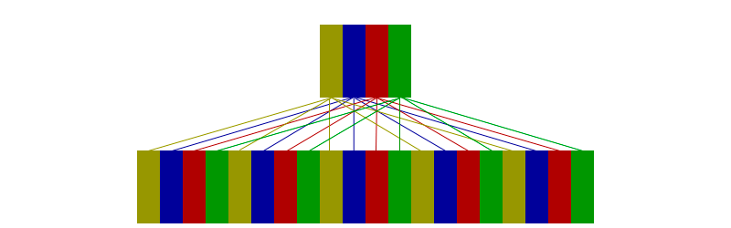
Each cache element contains the following information:
When requested to read, the cache divides the input address into two parts - a tag and an index. The size of the index is log (n), where n is the size of the cache.
The declaration of the cache module is identical to RAM, with the exception of the new output signal is_missrate. This output stores information about whether the last read request was missrate.
Before declaring the registers, we determine the size of the cache and index:
Next, we declare an array in which the data that we write and read will be stored:
We also need to store validity bits and tags for each item in the cache:
Registers into which the input address will be split:
Registers that store the input values on the previous clock (for tracking changes in input data):
Registers for updating the output signals after calculations in the always block:
Input Values for RAM:
Output values for RAM:
Declaring a RAM module and connecting input and output signals:
Register initialization:
To begin with, for each clock we have two states - the input data is changed or not changed. Based on this, we have the following condition:
Block 1. In case the input data is changed, the first thing we do is reset the readiness status to 0:
Next, we update the registers that stored the input values of the previous clock:
We break the input address into a tag and index:
To calculate the tag, a bitwise shift to the right is used, for the index, it is enough to simply assign, because Extra bits of the address are not taken into account.
The next step is to choose between writing and reading:
In the case of recording, we initially modify the data in the cache, then update the input data for RAM. In the case of reading, we check for the presence of this element in the cache and, if it exists, write it to out_reg, otherwise we access RAM.
Block 2. If the data has not been changed since the previous clock was executed, then we have the following code:
Here we are waiting for the completion of the access to RAM (if there was no access, ram_response is 1), we update the data if there was a read command and set the cache readiness to 1.
And last, update the output values:
Before proceeding with code parsing, it is recommended that you learn the basic syntax of Verilog.
Here you can find training materials .
RAM
Step 1: declaring the module with the corresponding input / output signals
module ram ( input [word_size - 1:0] data, input [word_size - 1:0] addr, input wr, input clk, output response, output [word_size - 1:0] out ); parameter word_size = 32; - data - data to write.
- addr - address to the memory in RAM.
- wr - status (read / write).
- clk - clock cycle system.
- response - RAM readiness (1 - if RAM processed the read / write request, 0 - otherwise).
- out - data read from RAM.
This implementation was integrated into Altera Max 10 FPGA, which has a 32-bit architecture, and therefore the size for data and address (word_size) is 32 bits.
')
Step 2: declaring the registers inside the module
An array declaration for storing data:
parameter size = 1<<32; reg [word_size-1:0] ram [size-1:0]; We will also need to store the previous input parameters in order to track their changes in the always block:
reg [word_size-1:0] data_reg; reg [word_size-1:0] addr_reg; reg wr_reg; And the last two registers for updating the output signals after calculations in the always block:
reg [word_size-1:0] out_reg; reg response_reg; We initialize the registers:
initial begin response_reg = 1; data_reg = 0; addr_reg = 0; wr_reg = 0; end Step 3: implementing the always logic of the block
always @(negedge clk) begin if ((data != data_reg) || (addr%size != addr_reg)|| (wr != wr_reg)) begin response_reg = 0; data_reg = data; addr_reg = addr%size; wr_reg = wr; end else begin if (response_reg == 0) begin if (wr) ram[addr] = data; else out_reg = ram[addr]; response_reg = 1; end end end Always block is triggered by negedje, i.e. at the moment the clock moves from 1 to 0. This is done to correctly synchronize the RAM with the cache. Otherwise, there may be cases when the RAM does not have time to reset the ready status from 1 to 0 and at the next clock, the cache decides that the RAM has successfully processed its request, which is fundamentally wrong.
The logic of the always block algorithm is as follows: if the data is updated, reset the readiness status to 0 and write / read data, if the write / read is completed, we update the readiness status to 1.
At the end, add the following code section:
assign out = out_reg; assign response = response_reg; The type of output signals of our module is wire. The only way to change signals of this type is long-term assignment, which is forbidden inside the always block. For this reason, the always block uses registers, which are subsequently assigned to the output signals.
Direct mapping cache
Direct mapping cache is one of the simplest types of cache. In this implementation, the cache consists of n elements, and RAM is conditionally divided into blocks by n, then the i-th element in the cache corresponds to all such k-th elements in RAM that satisfy the condition i = k% n.
The image below shows a cache of size 4 and RAM size of 16.
Each cache element contains the following information:
- validity bit - whether the information in the cache is relevant.
- tag is the block number in RAM where this element is located.
- data - information that we write / read.
When requested to read, the cache divides the input address into two parts - a tag and an index. The size of the index is log (n), where n is the size of the cache.
Step 1: declaring the module with the corresponding input / output signals
module direct_mapping_cache ( input [word_size-1:0] data, input [word_size-1:0] addr, input wr, input clk, output response, output is_missrate, output [word_size-1:0] out ); parameter word_size = 32; The declaration of the cache module is identical to RAM, with the exception of the new output signal is_missrate. This output stores information about whether the last read request was missrate.
Step 2: declaring the registers and RAM
Before declaring the registers, we determine the size of the cache and index:
parameter size = 64; parameter index_size = 6; Next, we declare an array in which the data that we write and read will be stored:
reg [word_size-1:0] data_array [size-1:0]; We also need to store validity bits and tags for each item in the cache:
reg validity_array [size-1:0]; reg [word_size-index_size-1:0] tag_array [size-1:0]; reg [index_size-1:0] index_array [size-1:0]; Registers into which the input address will be split:
reg [word_size-index_size-1:0] tag; reg [index_size-1:0] index; Registers that store the input values on the previous clock (for tracking changes in input data):
reg [word_size-1:0] data_reg; reg [word_size-1:0] addr_reg; reg wr_reg; Registers for updating the output signals after calculations in the always block:
reg response_reg; reg is_missrate_reg; reg [word_size-1:0] out_reg; Input Values for RAM:
reg [word_size-1:0] ram_data; reg [word_size-1:0] ram_addr; reg ram_wr; Output values for RAM:
wire ram_response; wire [word_size-1:0] ram_out; Declaring a RAM module and connecting input and output signals:
ram ram( .data(ram_data), .addr(ram_addr), .wr(ram_wr), .clk(clk), .response(ram_response), .out(ram_out)); Register initialization:
initial integer i initial begin data_reg = 0; addr_reg = 0; wr_reg = 0; for (i = 0; i < size; i=i+1) begin data_array[i] = 0; tag_array[i] = 0; validity_array[i] = 0; end end Step 3: implementing the always logic of the block
To begin with, for each clock we have two states - the input data is changed or not changed. Based on this, we have the following condition:
always @(posedge clk) begin if (data_reg != data || addr_reg != addr || wr_reg != wr) begin end // 1: else begin // 2: end end Block 1. In case the input data is changed, the first thing we do is reset the readiness status to 0:
response_reg = 0; Next, we update the registers that stored the input values of the previous clock:
data_reg = data; addr_reg = addr; wr_reg = wr; We break the input address into a tag and index:
tag = addr >> index_size; index = addr; To calculate the tag, a bitwise shift to the right is used, for the index, it is enough to simply assign, because Extra bits of the address are not taken into account.
The next step is to choose between writing and reading:
if (wr) begin // data_array[index] = data; tag_array[index] = tag; validity_array[index] = 1; ram_data = data; ram_addr = addr; ram_wr = wr; end else begin // if ((validity_array[index]) && (tag == tag_array[index])) begin // is_missrate_reg = 0; out_reg = data_array[index]; response_reg = 1; end else begin // is_missrate_reg = 1; ram_data = data; ram_addr = addr; ram_wr = wr; end end In the case of recording, we initially modify the data in the cache, then update the input data for RAM. In the case of reading, we check for the presence of this element in the cache and, if it exists, write it to out_reg, otherwise we access RAM.
Block 2. If the data has not been changed since the previous clock was executed, then we have the following code:
if ((ram_response) && (!response_reg)) begin if (wr == 0) begin validity_array [index] = 1; data_array [index] = ram_out; tag_array[index] = tag; out_reg = ram_out; end response_reg = 1; end Here we are waiting for the completion of the access to RAM (if there was no access, ram_response is 1), we update the data if there was a read command and set the cache readiness to 1.
And last, update the output values:
assign out = out_reg; assign is_missrate = is_missrate_reg; assign response = response_reg; Source: https://habr.com/ru/post/461611/
All Articles