Amateur radio technology: how I ordered the installation of a PCB in a Chinese factory
The purpose of the publication : to tell how to prepare a simple radio amateur design for production.
As I wrote earlier , the work of radio amateurs has a budget limited by the family and has a limit on the time taken from the family. Not every radio amateur can afford to have at home equipment for the manufacture of printed circuit boards and their installation. In the modern world, this is solved by CAD / CAM technologies, and CAM can be used for the manufacture of printed circuit boards and for the installation of components on these boards.
This article describes : how to install printed circuit boards in production; how to prepare in CAD Eagle 7.7.0 a project for assembling a prototype on a CAM located in the PRC.
')
This article does not consider : criteria for selecting a counterparty, economic aspects, logistics issues.
Preparation for production
The process of automated installation of a printed circuit board usually consists of the following steps:
- Manufacturing of printed circuit boards (PCB).
- Application to PCB soldering paste.
- PCB installation (Pick & Place) of SMD components.
- Melting solder paste in the oven.
- (If necessary) Installation on the bottom side of the SMD components board.
- (If necessary) Installation on the printed circuit board components THT (Through-Hole).
- Washing the assembled printed circuit assembly. Drying.
- Technical quality control of the installation of components.
- (If necessary) Repair the assembled printed circuit assembly.
- (If necessary) Coating.
How to make a printed circuit board in a Chinese factory, I described in a previous article in the cycle. When preparing a project for production, it is necessary to remember that:
- The printed circuit board must be rectangular. A non-rectangular printed circuit board must have a rectangular frame.
- Printed circuit boards are desirable to assemble in the panel. Small and non-rectangular printed circuit boards must be assembled in panels!
- Placing SMD components on only one side greatly simplifies and reduces the cost of the assembly process.
- The printed circuit board or panel should have enough free space around the components for mounting in the installer and the furnace.
- When applied to a printed circuit board solder paste is used stencil (stencil), which can be ordered together with the manufacture of printed circuit board.
- In order for the installer of the components to work correctly, reference signs must be applied to the printed circuit board (and / or on the technological fields of the panel).
- The range of components to download the installer is determined according to BOM (Bill Of Materials).
- Coordinates and orientation of components during installation (Pick & Place) contains a special file on the basis of which technologists create a task for the installer of components.
How I prepared my design for production
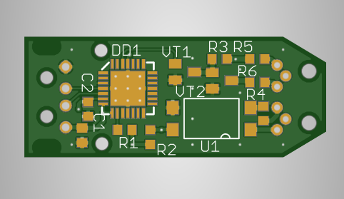
I decided to try to place an order for the assembly of a simple device from the article " Weekend Construction: A Simple MIDI Adapter ."
A simple and cheap SZOMK AK-S-27a was chosen as an adapter case. A small, rectangular-shaped PCB can be installed in this case.
Printed circuit boards for my amateur projects I usually order from pcbgogo.com . I decided to place an assembly order with them. Requirements for ordering the installation of printed circuit boards (PCBA) can be viewed here , samples of BOM files and Pick & Place can be viewed here .
The build process in PCBGOGO looks like this:

The minimum dimensions of the board are 50 * 100 mm. The minimum order for assembly is 5 printed circuit boards (panels), the minimum cost of work is $ 50 with a quantity of less than 20 printed circuit boards (panels). Stencil subject to order mounting is made free of charge. If the assembled panel fits into the preferential requirements for prototype boards, the manufacture of five or 10 such panels will cost $ 5.
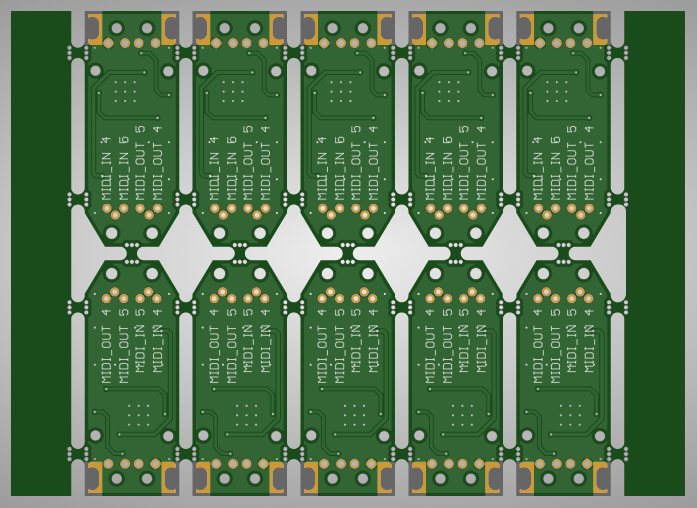
As a CAD in my amateur projects, I use the free version of Eagle 7.7.0 with a limited board size of 100 * 80 mm and the number of layers to two. I assembled the boards into the panel according to the instructions of Viktor's DIY Blog . The result was:

Since the panel assembled printed circuit boards of non-rectangular shape, they are separated by milling. Mill thickness in our case is 2 mm. A thin place jumpers - not less than 1.5 mm. The lintels are perforated with 0.5 mm drill bits with three holes on each side. The holes do not extend beyond the contours of the board, so that when removing the jumpers, no hemp is formed, and the edges of the board would not have to be processed before installation into the case.
If the panelable boards would be rectangular, they could be separated by scribing (v-scoring). Read more about scribing here .
The size of the panel turned out to be 100 * 72 mm. I located the SMD components on one side only. I oriented the boards in the panel in order to provide installation of USB output connectors without disassembling the panel. Technological fields on the left and on the right are intended for panel fastening in the production process. The requirement of the manufacturer to the minimum size of the board, not less than 50 * 100 mm, was fulfilled.
I did not apply the reference points to the panel: it was interesting what Chinese technologists would say to this!
Attention, spoiler
Chinese technologists have said nothing. They seem to be not the first time.
The initial data for the Pick & Place file was obtained as a result of exporting data from the panel project to the Mount SMD file format. From there, data on the positional notation of the components for the BOM were also taken.
It is necessary to pay attention to the fact that the reference designations of the same components in the BOM and Pick & Place files must completely coincide.
It should also be noted that component descriptions (component type, component manufacturer, nominal, footprint, etc.) are entered into the Pick & Place file for a more complete understanding by technologists of what this component is and how to install it correctly on the board.
A draft production-ready MIDI adapter panel is here .
Preparation for production by the manufacturer
After checking the project files, PCBGOGO technologists asked me
I ordered the complete set of the order to the manufacturer. Usually, when negotiating a BOM, they suggest replacing components with similar ones from other manufacturers or close ratings. In my case with BOM it was all simple: all the components found in the manufacturer's warehouse.
It should be noted that the customer can provide components for installation himself, but under the conditions of the manufacturer, the components must be sent in this case with a certain margin , and in our case also through customs. Unused trim will be returned with the order.
Visible to the customer part of the process of preparation for production by the manufacturer is over. Now that the process has been launched, I have to monitor the on-line order fulfillment and wait for the assembled printing units and stencil to be delivered to me.
Brief summary
This publication explores : the process of preparing a simple radio amateur design for production.
To order PCB fabrication and prototype assembly at a Chinese factory:
- Get acquainted with the requirements of the manufacturer.
- If necessary, assemble the printed circuit boards into the panel independently or provide it to the manufacturer.
- Unload files from the gerber project.
- Prepare BOM (Bill Of Materials).
- Prepare data for the installer component.
- Send project files to the manufacturer and coordinate with him the details.
- Pay the manufacturer production, packaging and delivery.
I really hope that the experience of ordering the installation of printed circuit boards described in the publication will help readers in organizing their technical creativity. And I also hope that any evaluation of the article will be accompanied by a comment.
73! Before communication!
Source: https://habr.com/ru/post/459850/
All Articles