The Las Vegas trade show is for electronics developers, not consumers. A report from Design Automation Conference

I decided to write this note on Habré in Russian and in English, in order to distribute a link to it both in English and Russian-speaking forums and groups. The Russian text is not a translation of English and vice versa - I just wrote a note twice (I hate to translate). Those who want to criticize my English immediately go to the end of the post, where they will be shocked by my accent in a long, hours-long video. I consider my accent not as a bug, but as a feature. We all know that many American women find, for example, the nasopharyngeal British accent attractive. It is time to give the same status and severe Russian accent. To do this, as many Russians as possible should make speeches at various international events. Our password is “years mi spik frome may hart”.
But first about the exhibition.
')
Millions of gadget consumers around the world are watching the Consumer Electronics Show (CES), which is being held in Las Vegas in January. They, who never knew what a D-trigger is, think it is important that four gigahertz are better than three in the latest processors from AMD and Qualcomm. But there is an exhibition focused not on consumers, but on electronics developers. This exhibition is called Design Automation Conference (DAC), and in some years it also takes place in Las Vegas, but not in December, but in June.
Millions of gadget lovers every year watch the Consumer Electronics Show (CES) which takes place in Las Vegas in January. It is a question of a technical publication. However, there is another conference, not for consumers, but for the creators of electronics. It is also a conference in the United States of America.
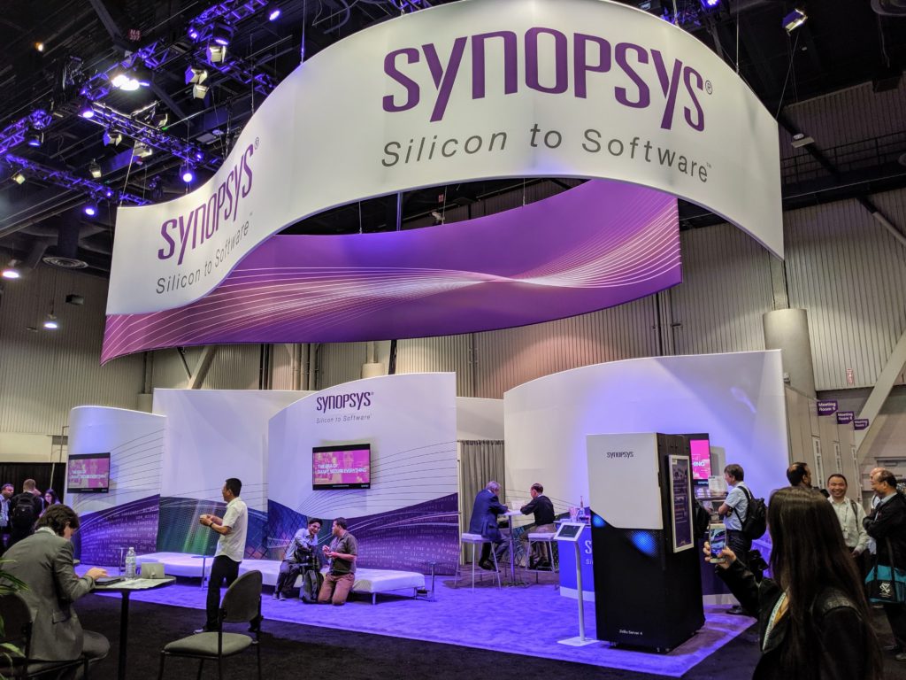
The industry of Electronic Design Automation (EDA) makes software for hardware designers. EDA is controlled by three large companies: Synopsys, Cadence and Mentor Graphics (now a part of Siemens). Both synopsys and cadence have a complete set of products. The design flow is called RTL2GDSII, it starts from the specification, coding it out, then it goes to the physical list. connect the standard cells and the building blocks of the ASICs (Application-Specific Integrated Circuits).
The electronics engineering automation industry is dominated by three large companies: Synopsys, Cadence and Mentor Graphics (which Siemens bought a couple of years ago). Synopsys and Cadence have created software that covers the entire RTL2GDSII design route. I briefly described this route in my previous article about the DAC four years ago:
Over the past25–30years, chip design has most often been written in the Verilog hardware description language (in Europe and in the military — VHDL), after which a special program (logic synthesis) turns the design into a graph of wires and logical primitives, another program (static timing analysis) informs the designer whether he fits into the speed budget, and the third program (place-and-route) lays out this design on the chip site.
When the design goes through all the stages: coding on the chain, debugging, verification, synthesis, static timing analysis, floorplanning, place-n-route, parasitics extraction, etc. - it turns out a file called GDSII, which is sent to the factory, and the factory bakes chips. The most famous factories of this type are owned by Taiwan Semiconductor Manufacturing Company or TSMC.

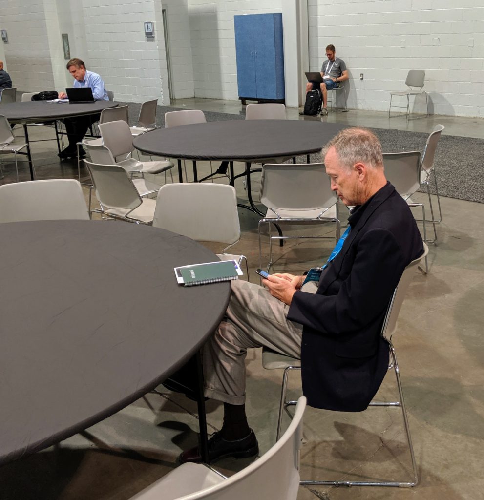
John Sanguinetti, a Verilog guru since the 1980s. Chronologic Simulation, which was created by VCS, a Verilog Compiled code Simulator. This simulator is now a property of Synopsys. VCS is used by large electronic companies. VCS brought to Synopsys billions dollars in revenue.
John Sanguinetti, the early guru of the velooga from the 1980s and the founder of the company Chronologic Simulation, is sitting apart from the exhibition hall. This company presented the world with a fast simulator of the Verilog Compiled code Simulator, which is now owned by Synopsys. This simulator is used by most major chip developers. VCS brought Synopsys billions of dollars:
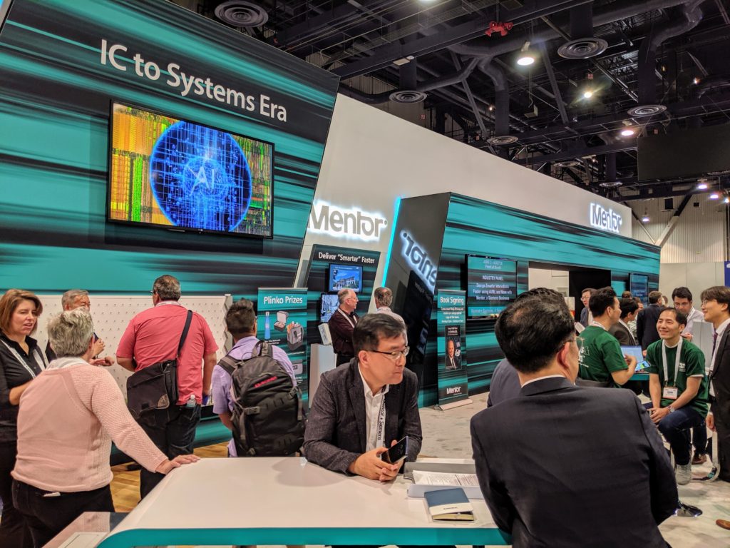
Mentor Graphics is the third-largest EDA company. Unlike Synopsys and Cadence, Mentor Graphics does not have a full line of RTL2GDSII tools. Calibre, a set of physical design tools, and a hardware emulator. Caliber includes: Veloce uses FPGA-like chips that
Mentor Graphics, the third largest company in the EDA industry, at the end of 2016 became part of Siemens. Unlike Synopsis and Kaydensa, Mentor does not have the entire chain of programs that cover the route RTL2GDSII. The two major sources of income for Mentor are the Caliber software package, which makes checks at the final design stage of microchips, and the Veloce emulator (pronounced “Velochi”). An example of a check in Caliber is the minimum distance between tracks on a chip
UPD: corrected on the basis of amartology comment: Antenna is generally about something else. It occurs when one track becomes so large that it begins to work as an antenna, receiving during production a signal at the plasma oscillation frequency for etching.
And the Veloce emulator uses FPGA-shaped ASICs to quickly
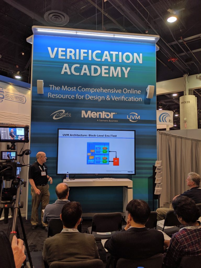
In addition to the highly profitable projects, Mentor has always been a large number of other projects, products, services, trainings and educational programs. For example, it is a critically important part of the digital design workflow.
In addition to highly profitable projects such as Caliber and Veloce, there are plenty of other projects, products, services, research projects and educational programs in Mentor. For example, in Mentor, functional verification is carried out - a crucial part of the production process:
A number of small companies, including Doulos, Willamette HDL and Sunburst Design, are selling hardware verification companies. There is no need to adopt new technologies, such as System Verification, UVM, Portable Stimulus, etc. Even Stanford doesn’t have to do with her graduates.
Functional verification feeds on several small companies that sell SystemVerilog and UVM trainings to large corporations at refreshingly high prices, such as a couple thousand dollars per person. They include Doulos, Willamette HDL, Sunburst Design and others:

Another small company called Verific. They are very successful in their niche. Verific sells SystemVerilog parsers adopted by important EDA companies, both large and small.
Here is another small, just a few people, but very successful company of its kind called Verific. She sells the Verilog parser, which is used by many EDA companies:

The EDA Cafe website is called the EDA Cafe. I like it a few days ago I’m not including John Cooley on DAC floor this time.
Here is the founder of Verific giving an interview to the popular EDA Cafe website:

Now let's talk about FPGA.
Now let's talk about the FPGA, they are PPMs (they will correct me now), they are FPGAs.
What it is, I also briefly described in my previous post about the DAC four years ago:
In its simplest form, an FPGA consists of a matrix of homogeneous cells, each function of which can be changed using multiplexers connected to the bits of the configuration memory. One cell can become an AND gate with four inputs and one output, the other one-bit register, etc. We load into the configuration memory a sequence of bits from the memory — and a predetermined electronic circuit is formed in the FPGA, which can be a processor, a display controller, etc.FPGA's two largest producers are Xilinx and Altera, now a part of Intel.
FPGAs / FPGAs are not processors, “programming” FPGAs (filling in the FPGA configuration memory) you create an electronic circuit (hardware), while programming a processor (fixed hardware), you slip a chain of sequential instructions written into the memory (software).
The two largest companies that produce FPGA are Xilinx and Altera, now part of Intel:
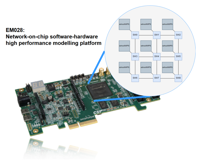
This week's round of the Innovate FPGA contest. One of the Russian entries is a mesh of schoolMIPS processor cores. schoolMIPS implements a subset of MIPS architecture. It exists in several variants, including a single-cycle data memory (a simplest one), a version with interrupts, a pipelined version, etc:
By the way, Intel is voting this week at the Innovate FPGA contest, which also includes Russian teams . One of the projects is the NoC-based multiprocessing system prototype . This is a prototype network on a chip with a large number of nodes based on Stanislav Zelio processors sparf (according to the book Harris & Harris “Digital Synthesis and Computer Architecture”) https://github.com/MIPSfpga/schoolMIPS . Does the student 4 courses MIEM HSE:
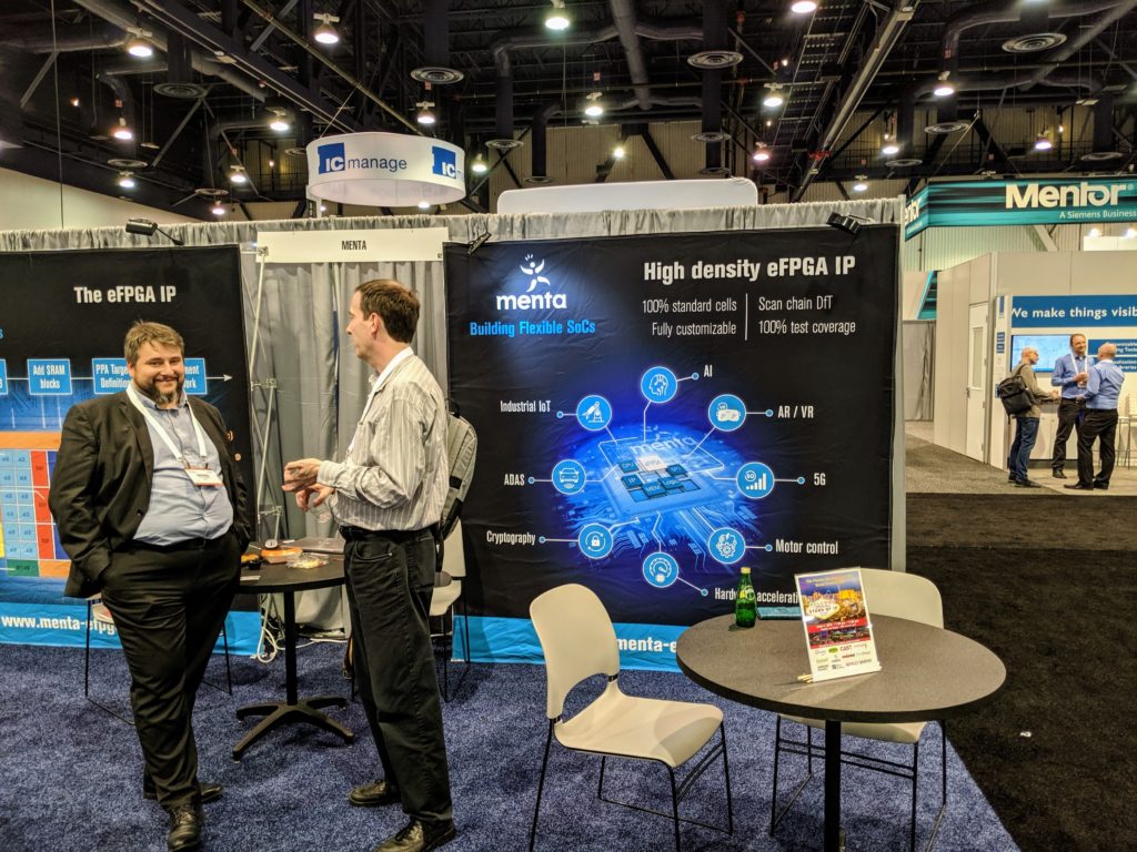
The World of FPGAs is not limited to Xilinx and Altera / Intel. There are also a small number of small and small companies. A coprocessor connected to a fixed high-frequency CPU core. Someone has been trying to find out what kind of time it is.
But there are smaller players in the FPGA world, for example, here are two companies that license the design of FPGA blocks that can be embedded in large-circulation fixed chips to give them flexibility.

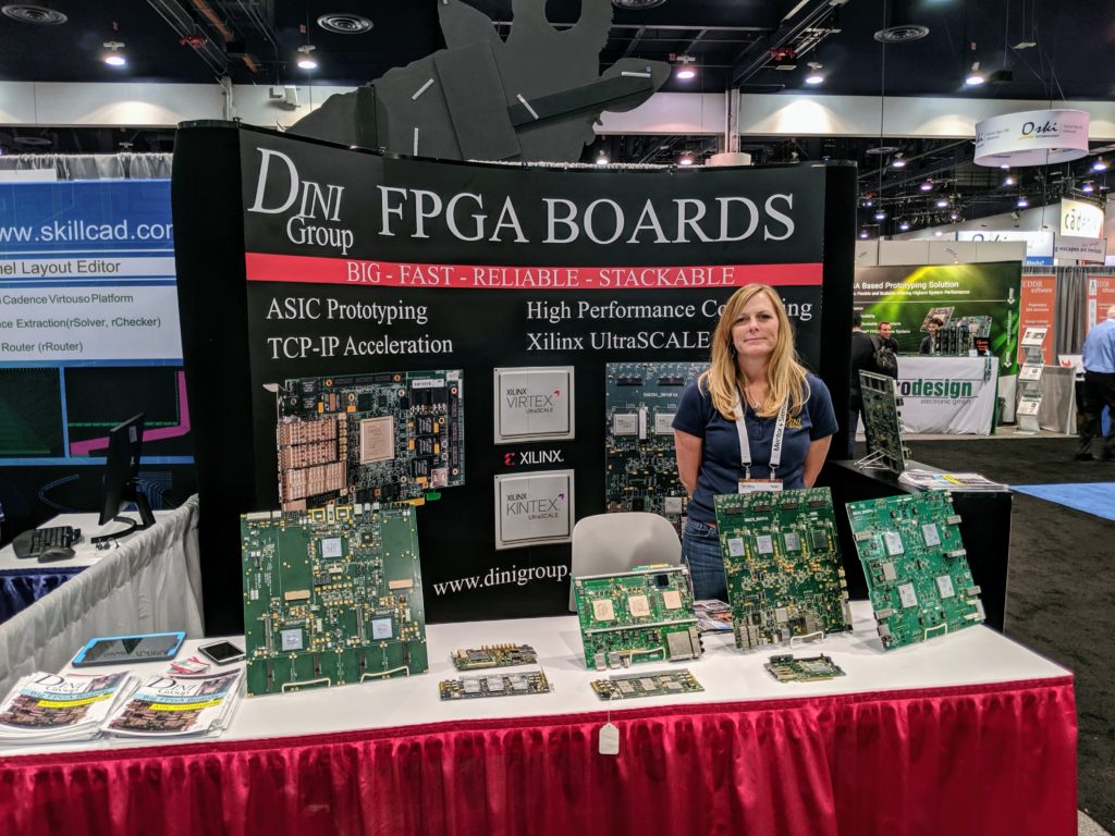
Every DAC has several FPGA board vendors. Do you need to pay for $ 30,000, or $ 100,000 or more.
On the DAC, manufacturers of FPGA boards are traditionally present. They are selling not cheap student fees for $ 55 dollars, but serious FPGA boards for $ 55 _ thousand dollars and above. Their client is not a student, but an austere ASIC development team that uses large fees for prototyping.
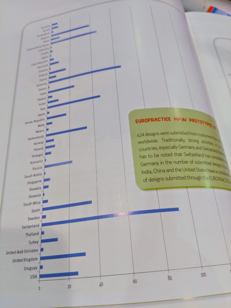
What if a researcher didn’t need any proof of concept using FPGA and now wants to manufacture its own ASIC? A typical commercial order to manufacture an ASIC usually requires the initial payment from ~ $ 300K to ~ $ 3,000,000 depending on process technology. However, there is a small number of shuttle services, or a multi-project wafer (MPW) services, 28nm.
But what if a student or a harsh company wanted to make a real ASIC in a factory, but you don’t have much or little money? Or, if it’s not a pity, is it a test chip or a very small batch? To do this, in America there is the company MOSIS, and in Europe - Europractice. Several thousand dollars - and you have in your hands a chip designed by you on a technology like 180 nanometers. A couple of tens of thousands - and you have your chip on the latest technology, for example, 28 nanometers, like the fifth iPhone. I note that for mass commercial production, the initial payment to the factory ranges from hundreds of thousands of dollars for old technologies to two or three million for new ones.
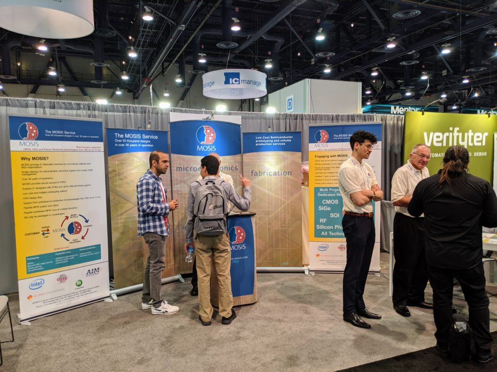
It is interesting that Europractice has customers in Russia, even in Omsk. Admit, who in Omsk designs ASIC-i.
Europractice has a number of Russian companies, including somebody in Omsk:
There are some business models that are mysterious to me. For example, I do not understand the Eclipse plugin. I guess they get the most revenue selling some consulting services.
There are companies about which I do not understand how they earn. For example, this one sells a very niche plugin to Eclipse. Surely they do not live on him, but on some consulting.
Another niche company with a non-obvious business model. They are a software of registers into software and other interface files. I’m guessing you’ve gotten a lot of Cisco-type customer.
Another niche company with an unobvious business model. They translate the description of the registers available to the programmer into verilog and interface files. Probably, they have some large client like Cisco, which once many years ago sunk into their tools, and since then has been paying, because the client’s management has failed to hire his engineer.

A melancholic gentleman from Huawei described their achievements in networking chips. Huawei is obviously dependent on the US EDA tools, even more than the ARM CPU cores. It is much more than a competitor for ARM cores.
At the exhibition, a representative of Huawei sat with an expression of light sadness on his face. I note that if the US government forces American EDA companies to ban Chinese, the Chinese situation will be much worse than it is now, as it is technically more difficult to clone the Synopsys IC Compiler than the ARM processor core and the Android Market.

Every DAC since 1998 was a C-to-Verilog compiler. Back in 1998 it was my own startup . This year it is somebody else:
At each DAC display since 1998, there has been at least one company that compiles C into Verilog. In 1998, such a company was my own startup. This year someone else:

This is a man who earns his life by the so-called “Zakladki” (a Russian term, a plurality of “Zakladka”). He agreed.
Here the companion earns his living by analyzing the bookmarks to the processors:

Daddy earns living:
I brought my daughter to Las Vegas to look at how people earn money in the harsh industrial world of the electronics industry, and I realized that my father's dollars are not growing on trees:

Party after the exhibition:
On the party after the exhibition:

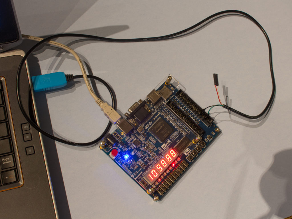
After the exhibition, I did a MIPS Open Developer Day together with my colleagues from Wave Comnputing. We have a number of people who want to go on business , and a Russian Silicon Valley. Digidant Nexys4 DDR and Terasic DE10-Lite FPGA boards.
Then I and my colleagues held a MIPS Open seminar. Comrades from some of the described companies came to him, including those that license the built-in FPGA and EDA tools, sell services for production, conduct training on verification, and also make chips as such. And also my old friends from the Russian company VivEng . My colleagues and I showed these slides , after which the participants tried examples on the FPGA boards of the Digilent Nexys4 DDR and Terasic DE10-Lite.
To repeat the results, you can download and combine two packages:
If you want to reproduce the results, you can do the following:
- Go to https://www.mipsopen.com/mips-open-components/mips-open-fpga-getting-started-guide .
- Download the standard MIPSfpga 2.0 package.
- Go to https://github.com/MIPSfpga/mipsfpga-plus .
- git clone github.com/MIPSfpga/mipsfpga-plus.git
- Copy Core RTL files from MIPS Open FPGA package to the subdirectory of the MIPSfpga + package - see instruction in https://github.com/MIPSfpga/mipsfpga-plus/tree/master/core
Your computer must have either the Intel FPGA Quartus Prime Lite Edition, or Xilinx Vivado, and the Codescape GCC Bare Metal Toolchain. After that you can follow the instructions from the slides:
You need to have the FPGA Quartus Prime Lite Edition or Xilinx. After this you can follow the instruction from the slides:
- cd your_git_directory / boards / board_directory (for example de10_lite or nexys4_ddr)
- make all load
- Press reset (or KEY 0 on some boards) to reset the processor.
- The default hardcoded program should start to work.
- cd your_git_directory / programs / 00_counter (or other program)
- make program srecord uart
- If your computer uses a serial connection, then the ttyUSB0 (the default), then:
- make program srecord uart UART = 1 (or 2, 3, etc)
- The program uploaded via USB-to-UART is now running.
In the presentation, I showed how to integrate into the processor a block that decodes and executes instructions additional to the main system of commands that the system designer on the chip can determine. The block can be synthesized and become part of the chip or be configured in FPGA / FPGA.
Additional instructions move along the processor pipeline along with the main ones. They get data from the general-purpose registers visible by the programmer and can return the result to the register. These instructions can also save a state in the coprocessor. They can be killed by exceptions if an exception occurs, for example, in the instruction following this instruction in the pipeline:
MIPS microAptiv UPC, FPGA board:
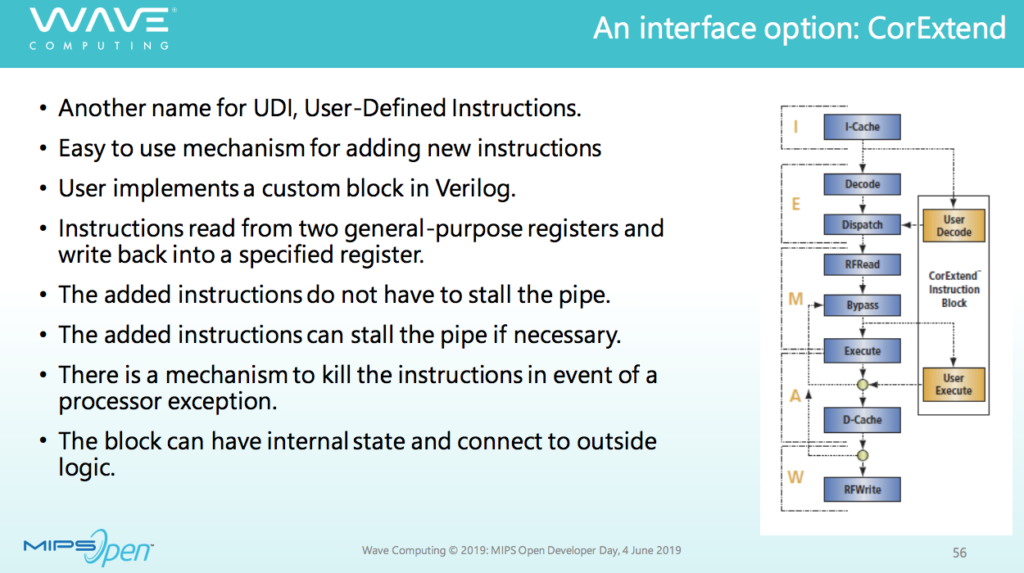
The code snippet in the Verilog hardware description language from the sample text. This code implements, at the Register Transfer Level (RTL), a specialized instruction for calculating a convolutional neural network:
CorExtend module custom implements for a special case of neural net computation:

I am interested in exploring careers of digital microelectronic design. For this trip I have been able to create a simple 2D videoprocessor for the VGA. Learn the basics of the RTL methodology:
And next Monday , July 8, I will be teaching the basics of developing digital schemes for schoolchildren in Zelenograd .
For him, I wrote examples of the implementation of simple sprite graphics on FPGA. The scheme, synthesized from a verilog, draws sprites on a VGA screen.
Here is a working example in pure hardware ( source code on github ). Variant of sea battle, where the red satellite-torpedo hunts for the enemy blue cross:
An example of a combination of hardware and software is a salute from sprites. Hardware part and software part :
Yes, and I promised to post my speeches in Las Vegas. Here is a piece:
There are no crowds yet:
And the view of the street on the strip when it is getting dark, but there are no crowds yet:
I played a chance to gamble, so I played it at the airport in Las Vegas.
For all this time in Las Vegas, I have not played, since I went around the exhibition and talked about electronic topics, then I conducted a seminar. But while landing on the plane, I nevertheless noted, lost one dollar:
Source: https://habr.com/ru/post/458760/
All Articles