How processors are developed and manufactured: chip manufacturing
This is the third article in a series on designing CPUs. In the first article, we reviewed the architecture of the computer and explained its work at a high level. The second article talked about the design and implementation of some of the components of the chip. In the third part, we learn how architectural designs and electrical circuits become physical chips.
How to turn a bunch of sand into a modern processor? Let's figure it out.
Part 1: Basics of computer architecture (instruction set architecture, caching, pipelines, hyperthreading)
Part 2: CPU Design Process (Wiring Diagrams, Transistors, Logic Elements, Timing)
Part 3: Compiling and physical chip manufacturing (VLSI and silicon fabrication)
Part 4: Current trends and important future directions in the architecture of computers (sea of accelerators, three-dimensional integration, FPGA, Near Memory Computing)
')
As mentioned earlier, processors and all other digital logic are made up of transistors. A transistor is an electrically controlled switch that can be turned on and off by applying or disconnecting the voltage at the gate. We said that there are two types of transistors: nMOS devices pass current when the gate is turned on, and pMOS devices pass current when the gate is turned off. The basic structure of the processor is transistors created from silicon. Silicon is a semiconductor , because it occupies an intermediate position - it does not conduct current completely, but it is not an insulator.
To transform a silicon wafer into a practical electrical circuit by adding transistors, production engineers use a process called " doping ". Doping is the process of adding carefully selected impurities to the base silicon substrate to change its conductivity. The goal is to change the behavior of electrons so that we can control them. There are two types of transistors, and therefore, two main types of doping.
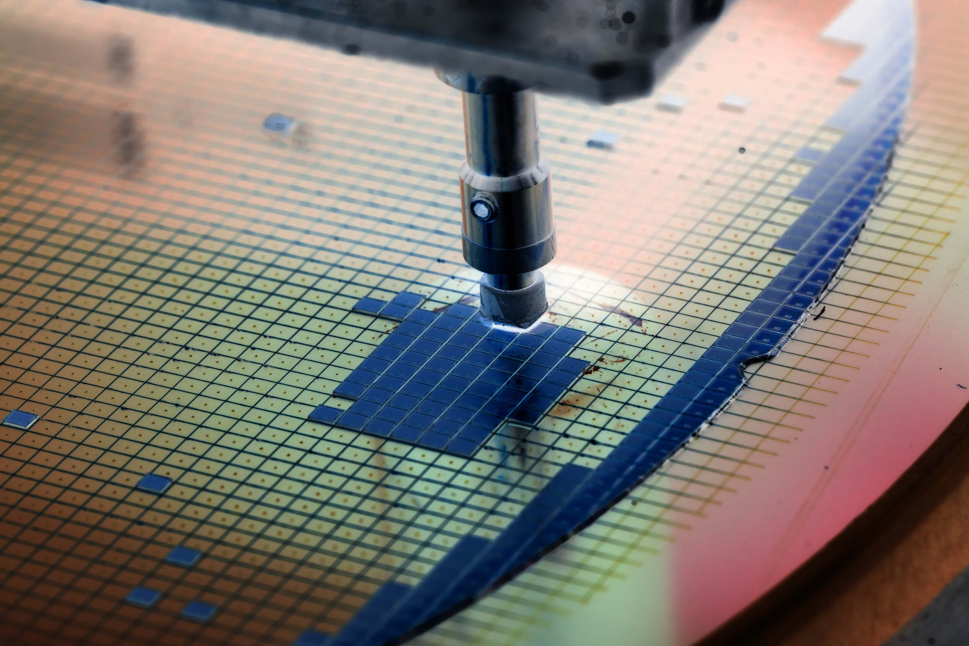
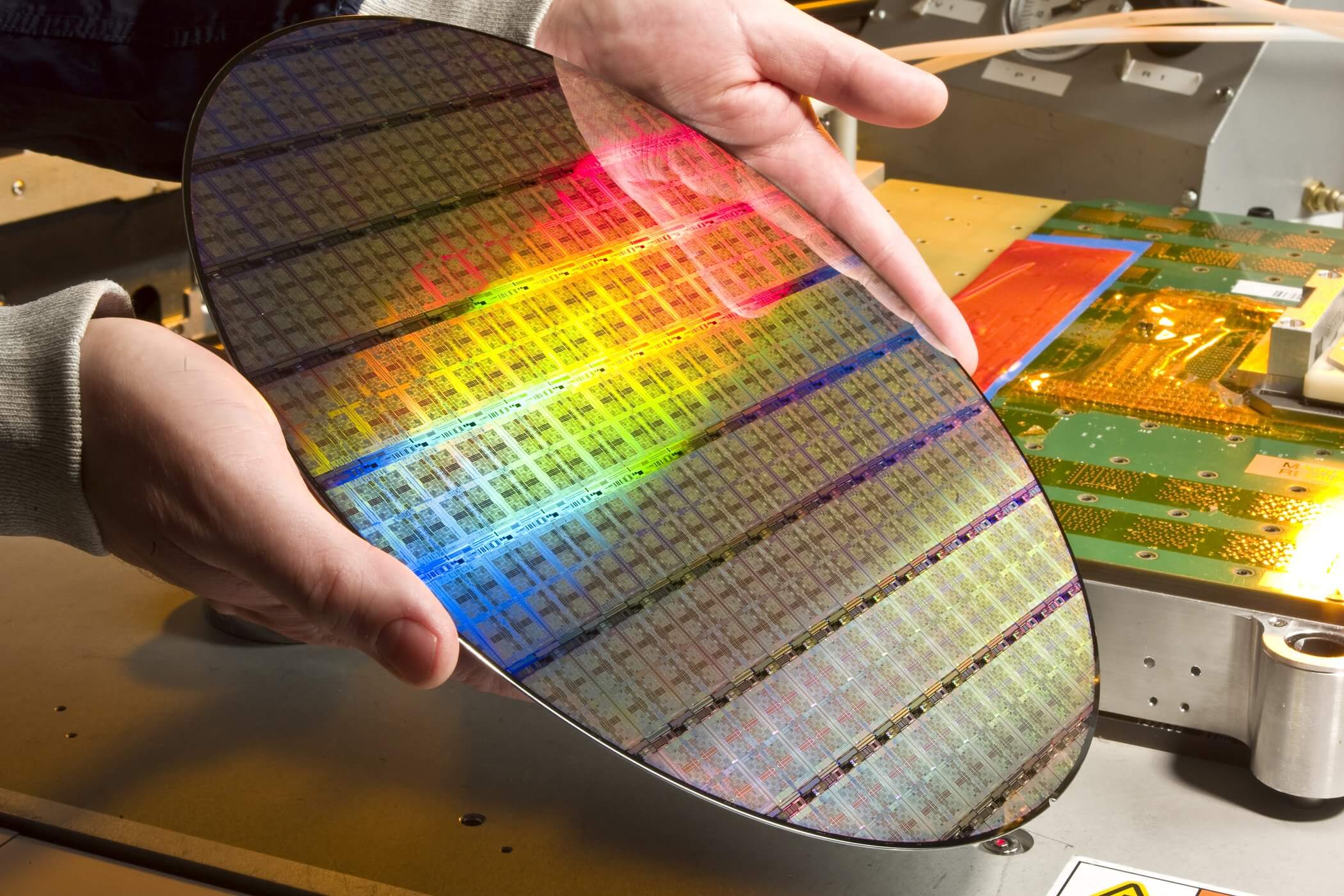
The process of making the plate before placing the chips in the case.
If we add a precisely controlled amount of electron donor elements, such as arsenic, antimony, or phosphorus, we can create an n-type region. Since the region of the plate on which these elements are deposited now has an excess of electrons, it becomes negatively charged. From here came the name of the type (n - negative) and the letter "n" in nMOS. By adding such electron acceptors as boron, indium or gallium to silicon, we can create a p-type region that is positively charged. From here came the letter "p" in the p-type and pMOS (p - positive). The specific processes of adding these impurities to silicon are called ion implantation and diffusion ; we will not consider them in the article.
Now that we can control the electrical conductivity of individual parts of the silicon wafer, we can combine the properties of several areas to create transistors. Transistors used in integrated circuits and called MOSFET (Metal Oxide Semiconductor Field Effect Transistors, MOS structures, metal oxide conductor structures) have four connections. The current we control flows between the source (Source) and the drain (Drain). In an n-channel device, current usually enters the drain and exits from the source, and in a p-channel device, it usually flows from the source and exits from the drain. A gate (Gate) is a switch used to turn the transistor on and off. Finally, the device has a transistor body (Body), which does not belong to the processor, so we will not consider it.
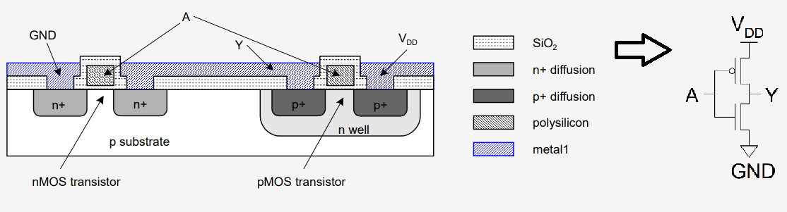
The physical structure of the inverter in silicon. Areas of different colors have different conductivity properties. Notice how the different silicon components correspond to the diagram on the right.
The technical details of the work of transistors and the interaction of individual areas is the content of the whole college course, so we will touch only the basics. A good analogy of their work is the drawbridge over the river. Cars - electrons in the transistor - they want to flow from one side of the river to the other, this is the source and drain of the transistor. Take for example the nMOS device: when the gate is not charged, the drawbridge is raised and the electrons cannot flow through the channel. When we lower the bridge, we will form a road over the river and the cars can move freely. The same thing happens in the transistor. Charging the gate forms a channel between the source and the drain, allowing current to flow.
For precise control over the location on silicon of different regions of p and n manufacturers, for example, Intel and TSMC use a process called photolithography . This is an extremely complex multi-step process and companies are spending billions of dollars to improve it in order to create smaller, faster and more energy-efficient transistors. Imagine an ultra-precise printer that you can use to draw patterns for each area on silicon.
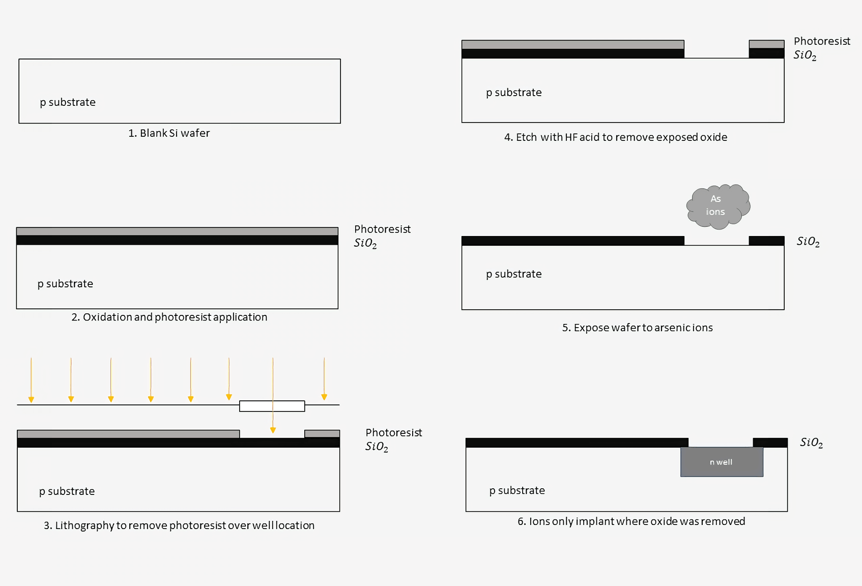
The process of manufacturing transistors on a chip begins with a clean silicon wafer (substrate). It is heated in a furnace to create a thin layer of silicon dioxide on the surface of the plate. Then a photosensitive photoresistive polymer is applied to the silica. Lighting the polymer with light of certain frequencies, we can expose the polymer in those areas where we want to do doping. This is a stage of lithography, and it is similar to how printers apply ink to certain areas of a page, only on a smaller scale.
The plate is etched with hydrofluoric acid to dissolve the silicon dioxide in the places where the polymer was removed. Then the photoresist is removed, leaving only the oxide layer below it. Now on the plate can be applied alloying ions, which are implanted only in places where there is no oxide.
This process of masking, shaping and doping is repeated dozens of times to slowly build each level of elements in a semiconductor. After completing the basic level of silicon on top, you can create metal connections connecting different transistors. A little later we will talk more about these compounds and layers of metallization.
Of course, chip manufacturers do not carry out the process of creating transistors under one. When designing a new chip, they generate masks for each stage of the manufacturing process. These masks contain the locations of each element of a billion transistor chip. Several chips are grouped together and made together on the same chip.
After making the plate, it is cut into individual crystals, which are placed
in the shell. Each plate can contain hundreds or even more chips. Usually, the more powerful a chip is produced, the larger the crystal will be, and the less chips a manufacturer can get from each plate.
You might think that we simply should produce huge super powerful chips with hundreds of cores, but this is impossible. Currently, the most serious factor preventing the creation of ever larger chips are defects in the production process. Modern chips contain billions of transistors and if at least one part of one transistor is broken, then the whole chip can be thrown out. As the size of the processors increases, the likelihood of a chip failure increases.
The efficiency of the manufacturing process of their chips companies carefully hide, but it can be roughly estimated at 70-90%. Companies usually make chips with a margin, because they know that some parts will not work. For example, Intel can design an 8-core chip, but only sell it as a 6-core chip, because it expects one or two cores to be broken. Chips with an unusually low defect count are usually set aside for sale at a higher price. This process is called binning .
One of the most serious marketing parameters associated with the manufacture of chips is the size of the elements. For example, Intel is mastering a 10-nanometer process, AMD is using a 7-nanometer for some GPUs, and TSMC has begun work on a 5-nanometer process. But what do all these numbers mean? Traditionally, the size of an element is called the minimum distance between the drain and the source of the transistor. In the process of technology development, we have learned how to reduce transistors so that they fit more and more on a single chip. When transistors are reduced, they also become faster and faster.
Looking at these numbers, it is important to remember that some companies can base the size of the process not on a standard distance, but on other values. This means that processes with different sizes for different companies can actually lead to the creation of transistors of the same size. On the other hand, not all transistors in a single process are the same size. Designers can decide for the sake of compromise to make some transistors larger than others. The fine transistor will be faster, because it takes less time to charge and discharge its gate. However, small transistors can control only a very small number of outputs. If some piece of logic will manage something that requires a lot of power, for example, an output pin, then it will have to be done much more. Such output transistors may be orders of magnitude larger than transistors of internal logic.
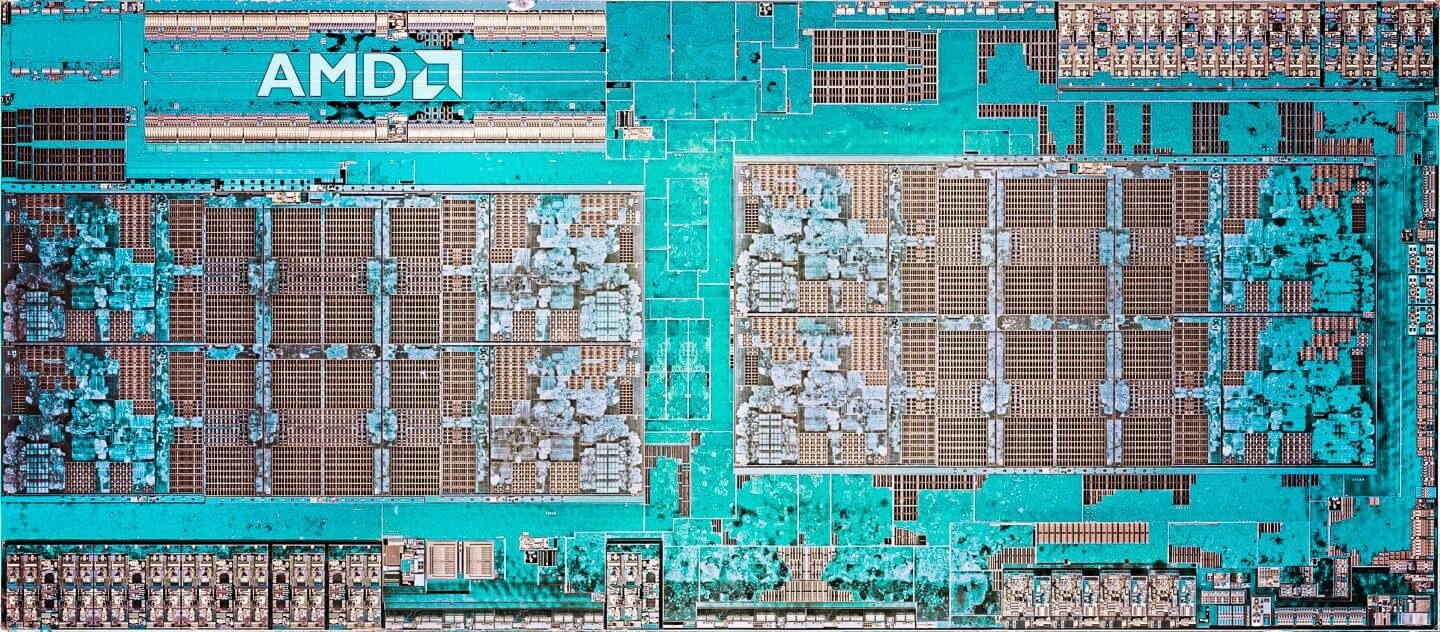
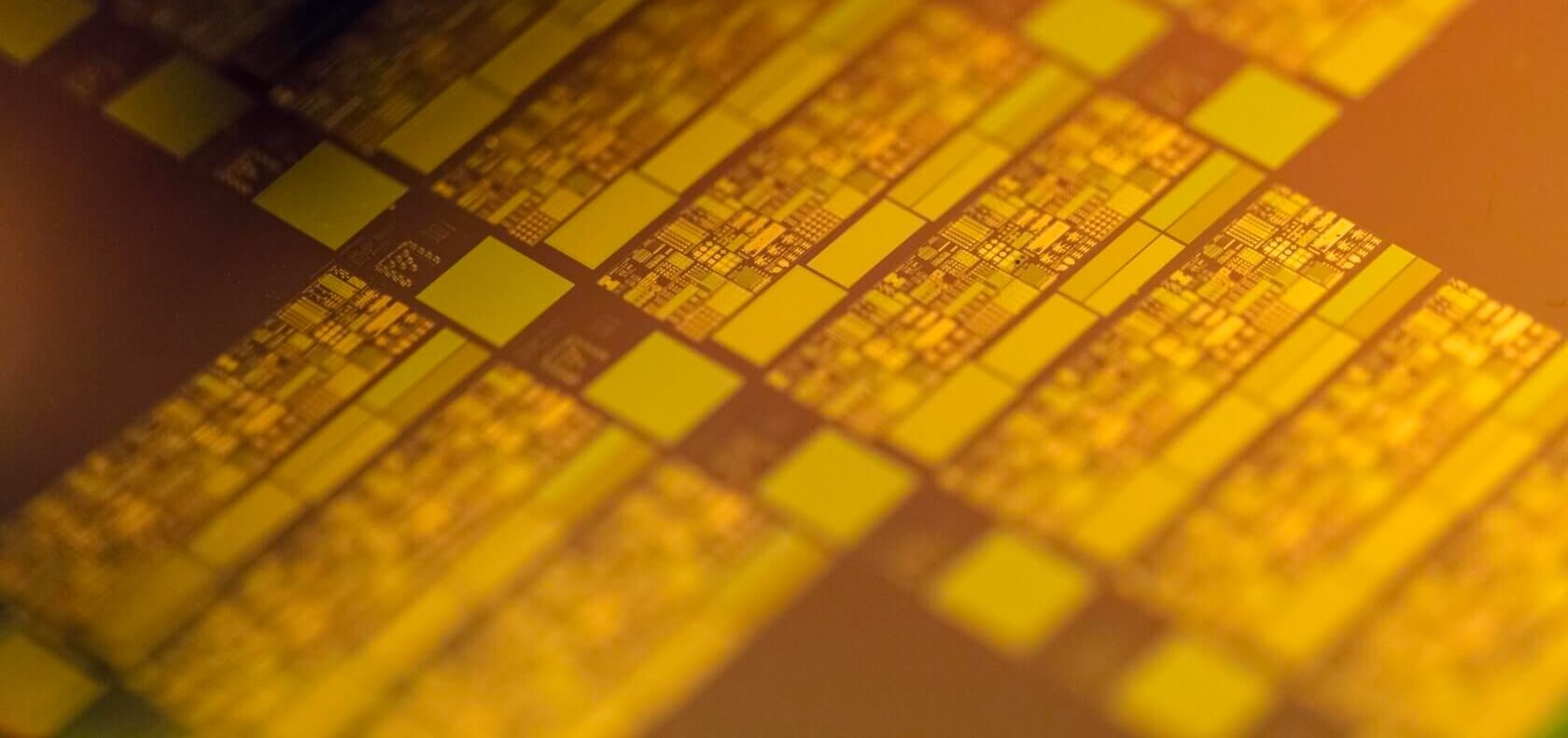
A snapshot of the crystal of the modern processor AMD Zen. This design consists of several billion transistors.
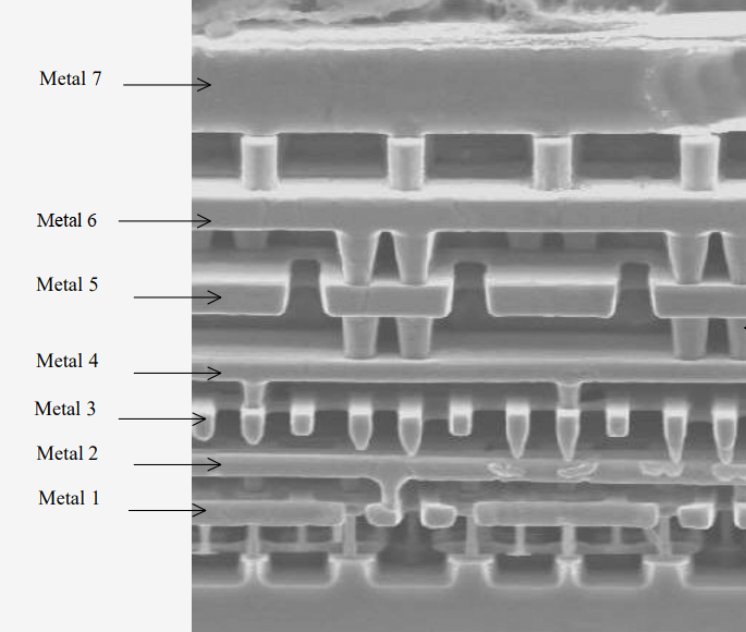
However, the design and manufacture of transistors is only half the chip. We need conductors to connect everything according to the scheme. These connections are created with the help of plating layers on top of transistors. Imagine a multi-level road junction with entrances, exits and a bunch of intersecting roads. That is what happens inside the chip, only on a much smaller scale. Different processors have a different number of metal bonding layers above transistors. Transistors are decreasing, and more signals are needed to route all signals. It is reported that in the future 5-nanometer process technology TMSC will be used 15 layers. Imagine a 15-level vertical road junction - this will give you an idea of how difficult the routing inside the chip is.
The microscope image shown below shows a grating formed by seven layers of metallization. Each layer is flat and as it rises, the layers become larger to help reduce resistance. Between the layers there are tiny metal cylinders called jumpers, which are used to move to a higher level. Typically, each layer changes direction relative to the layer below it, in order to reduce unwanted capacitance. Odd layers of metallization can be used to create horizontal joints, and even ones can be used for vertical joints.
It can be understood that the management of all these signals and metallization layers very quickly becomes incredibly difficult. To help solve this problem, computer programs are used that automatically locate and connect transistors. Depending on the complexity of the program design, they can even broadcast the functions of the high-level C code down to the physical locations of each conductor and transistor. Typically, chip designers allow computers to generate the bulk of a design automatically, and then examine and manually optimize individual critical parts.
When companies want to create a new chip, they begin the design process with standard cells provided by the chip manufacturer. For example, Intel or TSMC provide designers with basic parts such as logic elements or memory cells. Designers can combine these standard cells into any chip they want to produce. Then they are sent to the factory - the place where the raw silicon turns into working chips - electrical circuits of the transistors of the chip and metallization layers. These schemes turn into masks that are used in the manufacturing process described above. Next we look at how an extremely simple chip design process might look.
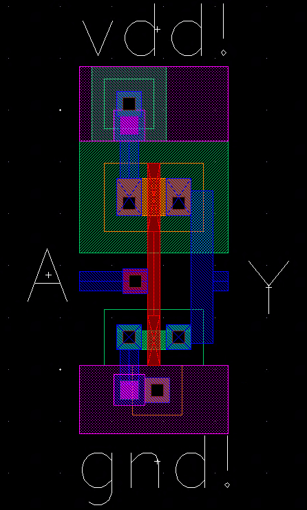
First we see the inverter circuit, which is a standard cell. The shaded green box at the top is a pMOS transistor, and the transparent green box at the bottom is an nMOS transistor. The vertical red conductor is a polysilicon gate, the blue areas are metallization 1, and the lilac areas are metallization 2. Input A is on the left and output Y is on the right. Power and ground connections are made at the top and bottom at the metallization 2.
Combining several logical elements, we got a simple 1-bit arithmetic module. This design can add, subtract, and perform logic operations with two 1-bit inputs. Upward shading blue conductors are the metallization layers 3. Slightly larger squares at the ends of the conductors are bridges connecting the two layers.
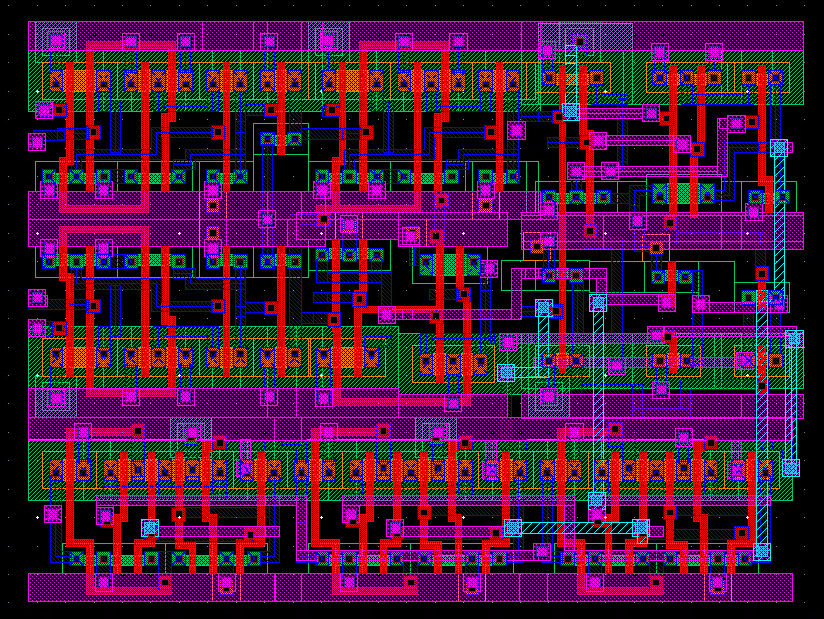
Finally, by combining many cells and approximately 2,000 transistors together, we got a simple 4-bit processor with 8 bytes of RAM on four layers of metallization. Having seen how complicated it is, one can only imagine how difficult it is to design a 64-bit processor with megabytes of cache, several cores and more than 20 stages of a pipeline. Considering the fact that modern high-performance CPUs have up to 5-10 billion transistors and a dozen layers of metallization, it would not be an exaggeration to say that they are literally millions of times more complicated than our example.
This makes us understand why the new processor is such an expensive piece of technology and why AMD and Intel have been releasing new products for so long. It takes 3-5 years for the new chip to go from the drawing board to the market. This means that the fastest modern chips are based on technologies that have been around for several years, and that we will not see chips for many years with the current level of manufacturing technology.
In the fourth and last article of the series, we will return to the physical sphere and consider current trends in the industry. What do researchers develop to make the next generation of computers even faster?
Source: https://habr.com/ru/post/457952/
All Articles