Universal memory: SRAM, DRAM and flash memory in one bottle
Nowadays there is not one type of memory, each of which is used for a particular task. They cope with their tasks quite well, but there are a number of shortcomings that do not make it possible to call any of these memory options universal. If we add here the problem of the colossal growth of data all over the world and the thirst of mankind for energy saving, then it is necessary to create something completely new. Today we will get acquainted with a study in which scientists presented a new type of memory, combining the advantages of both flash and DRAM memory. What kind of "buns" does this innovation have, what technologies have been used to create it and what are the prospects? We learn about it from the report of the research group. Go.
The basis of the study
There are far from one type of memory, and all of them were created for a specific task: SRAM (static random access memory) for the cache, DRAM (dynamic random access memory) for the active memory, flash memory for storing data, etc. However, which is quite expected, each of the above types of memory has its own personal flaws.
')
For example, flash memory, which is a set of MOS transistors (metal oxide semiconductor) with a floating gate (FG) for storing charge. The data are presented in such an embodiment as the amount of charge retained in FG, which is isolated by oxide layers.
The drawback, according to scientists, is that a sufficiently high voltage is required for recording and erasing to control the control gate (CG), usually around ± 20 V 2 . This process is slow, and the failure mechanism induced by a voltage surge leads to a reduction in the service life of the device.
Despite this minus, there is a rather impressive plus - the data is read by checking the conduction of the channel, for which very little voltage is needed. Due to this, the data remain intact, which is called non-destructive readout.
DRAM, in turn, is much faster than flash memory, and is therefore used for active computational processes, so to speak. The disadvantage of DRAM is that data is lost from cells when it is read. In addition, there are leakage of charge from the capacitors used for data storage.
SRAM is also a fairly fast type of memory and data is not as lost as in DRAM. However, as a rule, 6 transistors per cell are used, that is, you need a lot of area on the chip.
By presenting the above-described disadvantages of classic types of memory, scientists stress the importance of finding an alternative or hybrid version that will be free from such problems, while combining all the advantages of its predecessors.
In this work, the researchers present to our attention their vision of a new type of memory - a new low-voltage, semiconductor, charge-based, nonvolatile memory device of compact form, operating at room temperature. Researchers have christened their offspring "universal memory" (simply, but with taste).
The device is a floating gate memory created on the basis of InAs / AlSb / GaSb heterostructures, where InAs is used both as a floating gate and as a channel without transitions.
Scientists have provided simulation results and actual single-cell prototype tests.
Research results
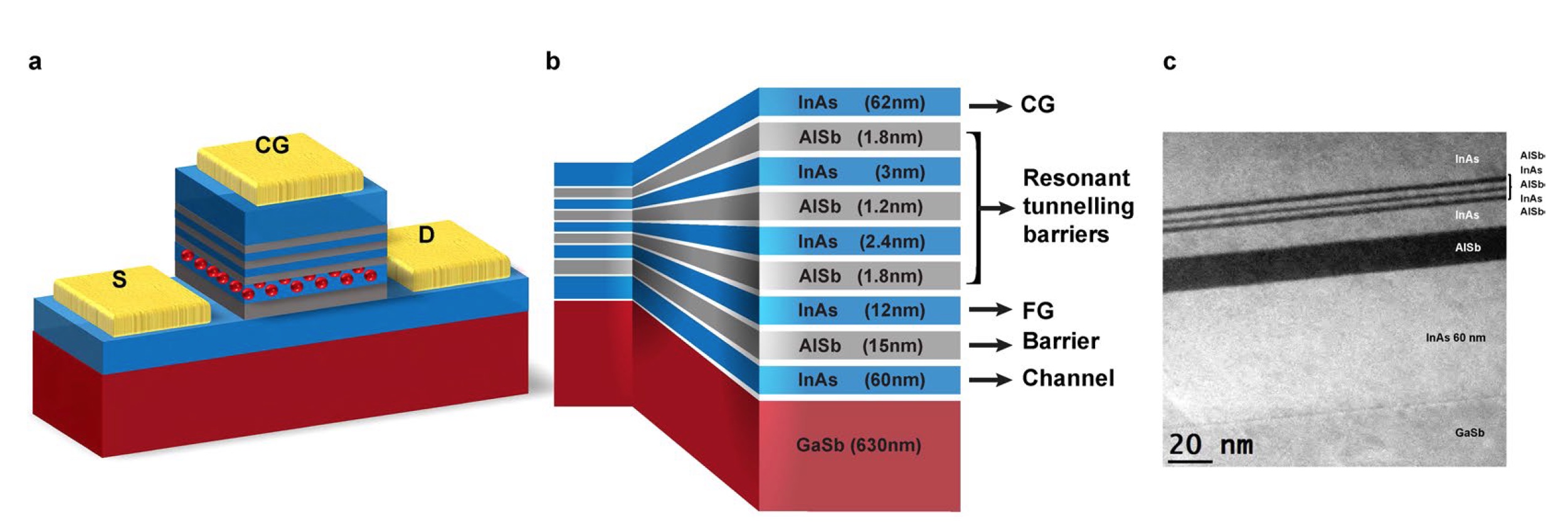
Image number 1
The image above shows a schematic view of the device and a PREM (transmission scanning electron microscope) image.
As in the case of flash memory, in this device the charge is stored in FG, but there are no oxide barriers. Instead, a shift in the conduction band in the so-called 6.1-Å family of semiconductors was used. That is, the device underlying the memory cell is more like a high electron mobility transistor (HEMT) than a MOS transistor. InAs forms a channel that does not contain transitions. However, n-doping was used to compensate for unintended background doping and to keep Ga vacancies in the underlying GaSb. Both of these tasks naturally make p-type layers.
pn junction * is the area of contact between two semiconductors with different types of conductivity - p (hole) and n (electronic).
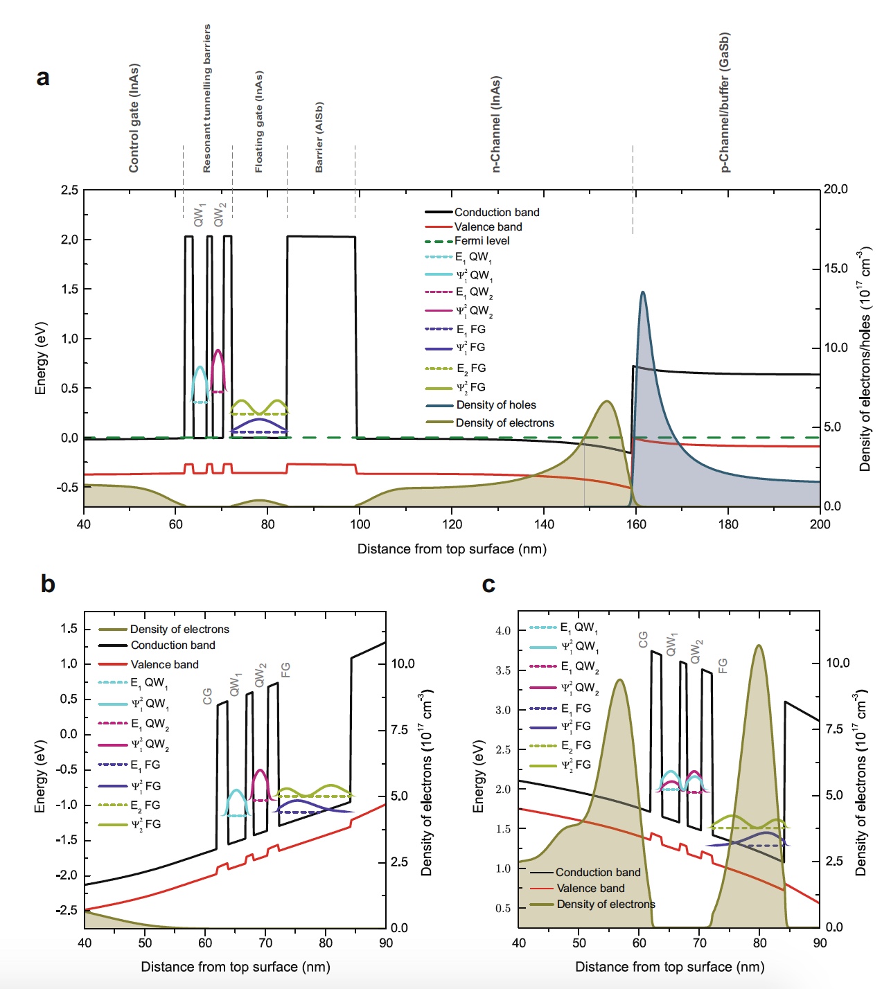
Image number 2
Graph 2a shows the modeled alignment of the energy bands, as well as the density of electrons and holes in the layers in the absence of displacement. Theoretical data in combination with modeling demonstrate that at the InAs and GaSb interface, the conduction band of InAs is below the valence band of GaSb. And this leads to the transfer of electrons from the GaSb layer to the InAs layer, after which holes remain in GaSb.
Hole * is an unfilled valence bond, manifesting itself as a positive charge equal to the electron charge.Accumulated electrons / holes are visible at the interface between InAs and GaSb, but electrons in the InAs channel are not connected to the InAs / GaSb interface, and their density is observed throughout the InAs. The conduction of the entire channel is dominated by electrons in InAs, which will have higher mobility and higher density than holes in GaSb.
The inner FG of the InAs layer is isolated from the InAs channel by the AlSb barrier (15 nm). At the same time, double InAs * QDs and three AlSb barriers play the role of a resonant tunneling barrier between FG and InG CGs with As-n-doping.
Quantum well * - restricts the movement of particles in a two-dimensional (instead of three-dimensional), because of which they can move only in a flat layer.Therefore, in the device under study, the electrons stored in the FG of the InAs layer are isolated by an anomalously large discontinuity of the conduction band with AlSb. This means that you can get a charge limiting system, which will have a storage time at room temperature, equal to 1014 years.
The most important aspect of the device under study is the fact that two quantum wells (QW1 and QW2) in a triple resonant tunneling barrier have different thicknesses, that is, limited states with different energies ( 2a ) occur. Since QW2 is thinner than QW1, the only available energy level for electrons in QW2 has a higher energy than the equivalent in QW1. In addition, the state in QW1 has a significantly higher energy than the state in the adjacent CG region. This prevents the direct tunneling of electrons between CG and FG, and the barrier to the transition of electrons from CG to FG (or vice versa) is determined by the displacement of the conduction band InAs / AlSb by 2.1 eV, that is, the charge will not flow to / from FG.
The ground and primary excited states in the floating gate (FG) are located well below the energy states within both QWs. Therefore, when no voltage is applied, the electrons are locked inside the FG, i.e. the triple resonant tunneling barrier becomes insurmountable for electrons to / from FG. Thus non-volatility is achieved.
If we apply a slight voltage to the control gate (CG), then we can adjust the connection of energy states inside the resonant tunnel barrier, which will allow electrons to freely pass from ( 2b ) or into ( 2c ) the floating gate.
During the experiments, all read, write, and erase operations were carried out in several cells (gate size 10 x 10 µm) in a dark box protected from electrostatics at room temperature. All operations, including recording and erasing, were performed at an offset of ≤ 2.6 V, which is about an order of magnitude lower than is necessary for full-fledged work with a flash memory cell, the researchers emphasize. Erasure was performed by shifting the control gate (V E CG-S ) by +2.5 or +2.6 V between the CG and the source, which resulted in a state of “0”.
Image 2b shows a simulated alignment of the energy zones obtained at an erasure voltage of +2.6 V. Under such circumstances, the calculated energy level of electrons in QW1 is lower than that in QW2, while both are below the first excited state and close to the energy level ground state in FG. The result of this is erasure, that is, the flow of electrons from FG to CG, followed by the depletion of FG. The same principle works for the write operation: V W CG-S = -V E CG-S to increase the charge in FG (state "1").
Graph 2c is a simulated energy zone when the control gate is used for recording data: V W CG-S = −2.6 V. In this case, the energy levels in QW1 and QW2 are almost the same, which leads to a strong connection between these states, resonant tunneling and flow electrons from CG to FG.
Due to the capacitive coupling, the conduction of the channel depends on the amount of charge stored in the FG, therefore data is read by measuring the gate-source current at a fixed gate-source voltage.
Charge increase in FG, i.e. state "1", reduces the charge in the channel, which leads to a decrease in its conductivity. In the case of the state "0" the reverse process occurs. Data reading can be done without any offset to the CG, but the voltage is necessary for individual sampling of devices in the array of cells. In addition, the voltage should generate an electric field at the resonant tunneling barrier, which will make it possible to transfer the charge from / to FG. To achieve these objectives will require only ~ 2.5 V.
Universal Memory Characteristics
During practical tests, the reading was performed with zero offset on CG and V SD = 1.0 V. However, according to the statements of scientists, it was possible to apply a lower voltage for successful reading.
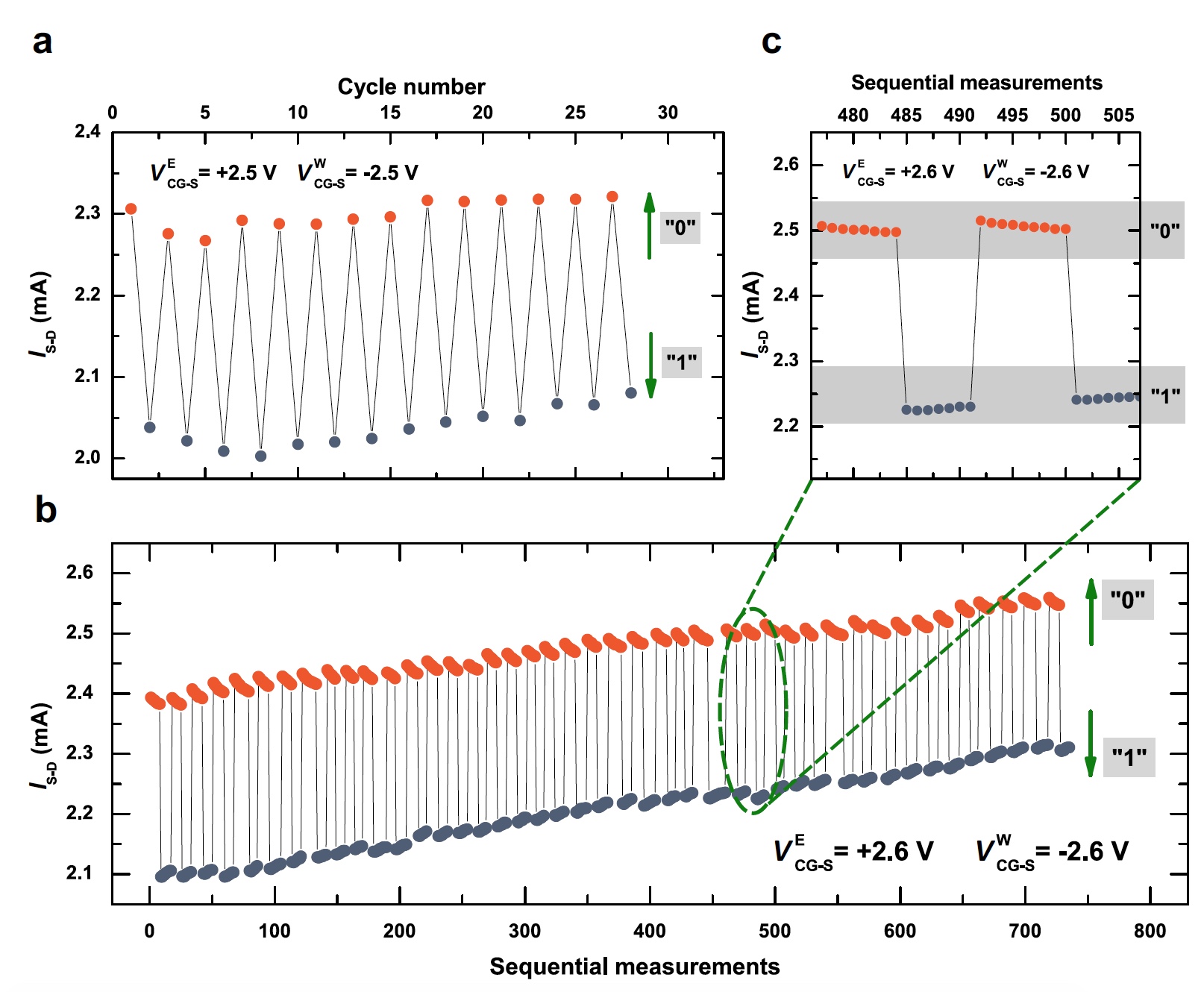
Image number 3
Figure 3a shows the erase-read-write-read flow. The main feature of the sequence is the read operation after each erase or write step.
Figure 3b shows a more complicated sequence in which, after each erase and write operation, there is not one read operation, but several. Thus, the researchers demonstrate that the reading operation is non-destructive.
Between the state "0" and "1" there is a clear difference in all sequences. However, at 3b there are signs of a symmetric upward shift in I SD as the number of operations increases. While the reason for this behavior is unclear, but scientists intend to investigate this aspect in further work. But on 3a this is not observed, since the voltage for erasing / writing is slightly lower.
After several hundred write and erase operations, as well as many reads during several practical tests, scientists did not find any signs of damage to the device.
An important feature of all types of memory, which are based on the storage of charge, is the switching energy, determined by the charging energy of the capacitor.
The similarity of the fundamentals of flash memory technology and the universal memory under study suggests comparing these two types of memory. If we assume that the two devices of these two types have the same capacity with the same shutter size, then the switching energy of the universal memory will be 64 times less than that of the flash memory. These amazing numbers also speak of the superiority of universal memory over DRAM.
According to theoretical estimates, the CG-FG capacitance is about 10 -12 F for a 10 x 10 µm device, and the switching energy is about 2 x 10 -12 J. A decrease in the physical size of the device drastically reduces the switching energy to 10 -17 J for a 20 device. nm, which is 100 times less than for DRAM, and 1000 times less than for flash memory. And this, according to the bold statements of the researchers, is very unique characteristics.
The image 3c shows some write-erase operations from 3b , where the state of “0” and “1” are visible: successive read measurements after erasing give a slightly smaller I SD for state “0”. The opposite situation is observed with successive read measurements after writing, or rather I SD is slightly larger.
Scientists attribute this effect to the variability (volatility) of the data. To study this, the scientists performed a sequence of reading operations over a long period of time for each state of memory (image No. 4).
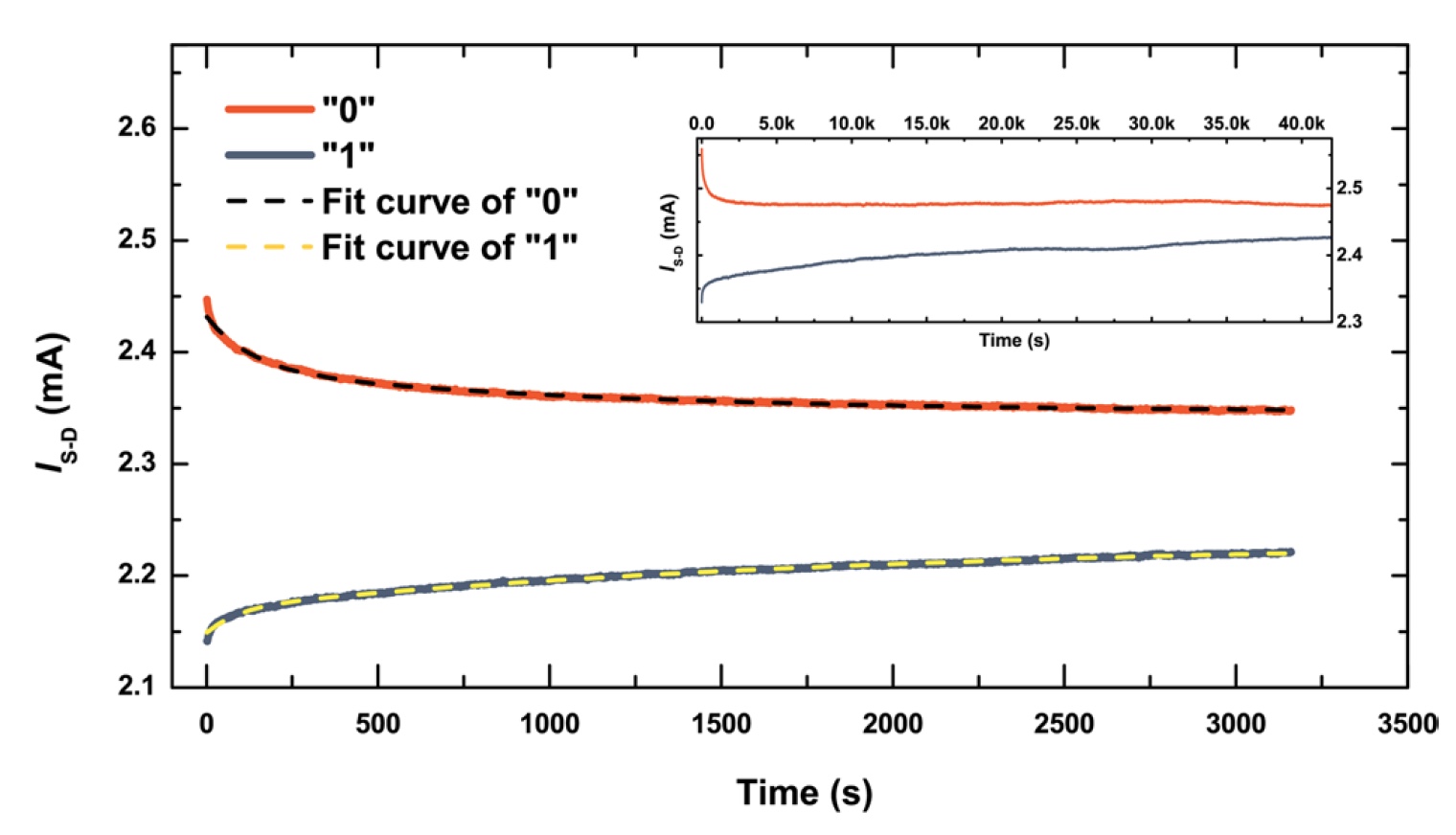
Image number 4
Both states “0” and “1” showed an initial rapid decay, which is consistent with what is seen in 3c . But after that, much slower changes occur, so that during the entire observation time the corresponding states “0” and “1” are clearly distinguishable.
Another experiment was also carried out (inset in image No. 4), which shows the limiting saturation of exponential decay and distinguishable states “0” and “1” in time.
The existence of double exponential decay means that several mechanisms lie at the heart of the degradation of states. Scientists identify tunneling through defective states in AlSb barriers, thermal excitation of electrons through a narrow InAs band gap, and recombination with thermally generated holes among the possible options.
An estimate of the capacity of the device and the applied write / erase voltage indicates that approximately 107 electrons are transferred from / to the floating gate during the write and erase operation. This is quite a lot, but the negative impact is practically not observed.
For a more detailed acquaintance with the nuances of the study I recommend to look into the report of the research group .
Epilogue
Scientists managed not only to develop a new type of memory, but also to conduct successful first practical tests of a non-volatile, charge-based device of compact size at room temperature. Scientists have also managed to combine energy independence and low-voltage switching by the quantum-mechanical properties of an asymmetric triple resonant tunneling barrier. Researchers claim that their device can be scaled without losing its value.
Times change, technology changes. Flash memory, SRAM and DRAM occupied a dominant position among the memory devices for a long time, but this may change if the development of universal memory continues just as successfully as in this study. This technology will greatly reduce the power consumption of devices equipped with it, as well as extend their service life and improve performance.
Further studies planned by the authors will show how revolutionary the memory is, so proudly called universal by scientists.
Thank you for your attention, stay curious and have a good working week, guys!
Thank you for staying with us. Do you like our articles? Want to see more interesting materials? Support us by placing an order or recommending to friends, 30% discount for Habr's users on a unique analogue of the entry-level servers that we invented for you: The whole truth about VPS (KVM) E5-2650 v4 (6 Cores) 10GB DDR4 240GB SSD 1Gbps from $ 20 or how to share the server? (Options are available with RAID1 and RAID10, up to 24 cores and up to 40GB DDR4).
Dell R730xd 2 times cheaper? Only we have 2 x Intel TetraDeca-Core Xeon 2x E5-2697v3 2.6GHz 14C 64GB DDR4 4x960GB SSD 1Gbps 100 TV from $ 199 in the Netherlands! Dell R420 - 2x E5-2430 2.2Ghz 6C 128GB DDR3 2x960GB SSD 1Gbps 100TB - from $ 99! Read about How to build an infrastructure building. class c using servers Dell R730xd E5-2650 v4 worth 9000 euros for a penny?
Source: https://habr.com/ru/post/457468/
All Articles