How processors are developed and manufactured: design of the CPU

Now that we know how processors work at a high level, it is time to delve into the analysis of the design process of their internal components. This is the second article in a series devoted to the development of processors. I recommend to study the first part for a start, so that you understand the concepts outlined below.
Part 1: Basics of computer architecture (instruction set architecture, caching, pipelines, hyperthreading)
Part 2: CPU Design Process (Wiring Diagrams, Transistors, Logic Elements, Timing)
Part 3: Compiling and physical chip manufacturing (VLSI and silicon fabrication)
Part 4: Current trends and important future directions in the architecture of computers (sea of accelerators, three-dimensional integration, FPGA, Near Memory Computing)
As you may know, processors and most other digital devices are made up of transistors. The easiest way to perceive the transistor as a controlled switch with three contacts. When the gate is turned on, electric current can flow through the transistor. When the shutter is off, the current cannot flow. The shutter is like a light switch in a room, only it is much smaller, faster and can be electrically controlled.
')
There are two main types of transistors used in modern processors: pMOS (PMOS) and nMOS (NMOS). The nMOS transistor transmits current when the gate (gate) is charged or has a high voltage, and the pMOS transistor passes the current when the gate is discharged or has a low voltage. By combining these types of transistors in a complementary way, we can create CMOS logic elements. In this article we will not discuss in detail the features of the work of transistors, but let us touch on this in the third part of the series.
A logical element is a simple device that receives input signals, performs some operation, and outputs a result. For example, the AND element (AND) turns on its output signal if and only if all the shutter inputs are on. The inverter, or the element NOT (NOT) turns on its output if the input is disabled. You can combine these two shutters and get an element NAND (NAND), which turns on the output, if and only if none of the inputs is turned on. There are other elements with their logical functionality, for example, OR (OR), OR-NOT (NOR), exclusive OR (XOR) and exclusive OR with inversion (XNOR).
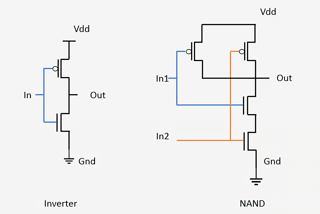
The following shows how two simple elements are assembled from transistors: an inverter and a NAND. In the inverter, the pMOS transistor (top) is connected to the power supply, and the nMOS transistor (bottom) is connected to ground. On the designation of pMOS transistors there is a small circle connected to the gate. We said that pMOS devices pass current when the input is turned off, and nMOS devices pass current when the input is turned on, so it's easy to see that the output signal (Out) will always be opposite to the input signal (In). Looking at the NAND element, we see that it requires four transistors, and that the output will always be turned off if at least one of the inputs is turned off. Similarly connecting transistors to form simple networks is the same process used to design more complex logic elements and other circuits inside processors.
Building blocks in the form of logical elements are so simple that it is difficult to understand how they turn into a functioning computer. The design process is to combine several elements to create a small device that can perform a simple function. You can then combine many of these devices to create something that performs a more complex function. The process of combining individual components to create a working structure is exactly the process that is used today to create modern chips. The only difference is that a modern chip consists of billions of transistors.
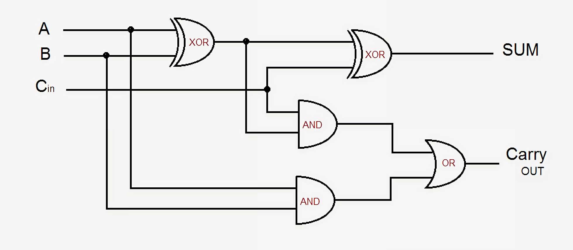
As a small example, let's take a simple adder - a 1-bit full adder. It receives three input signals - A, B, and Carry-In (transfer input signal), and creates two output signals - Sum (sum) and Carry-Out (transfer output signal). The simplest circuit uses five logical elements, and they can be connected together to create an adder of any size. In modern schemes, this process has been improved by optimizing a part of logic and transfer signals, but the fundamentals remain the same.
The output of Sum is either A, or B, but never both, or there is an incoming transfer signal, and then A and B are either both on or both off. The transfer output is a bit more complicated. It is active when either A and B are on at the same time, or there is Carry-in and one of A or B is on. To connect several 1-bit adders to create a wider adder, we just need to connect the Carry-out of the previous bit to the Carry-in of the current bit. The more complex the schemes become, the more confusing the logic is, but this is the easiest way to add two numbers. In modern processors, more sophisticated adders are used, but their schemes are too complex for such a review. In addition to adders, processors also contain devices for dividing, multiplying, and versions of all these floating point operations.
Such a combination of sequences of elements to perform a function on the input signals is called combinatorial logic . However, this is not the only type of logic used in computers. There will be no special benefit if we cannot store data or track status. In order to be able to save data, we need sequential logic.
Sequential logic is built by carefully connecting inverters and other logic elements so that their outputs transmit feedback signals to the elements. These feedback loops are used to store one bit of data and are called static RAM (Static RAM) , or SRAM. This memory is called static RAM versus dynamic memory (DRAM), because the stored data is always directly connected to a positive voltage or ground.
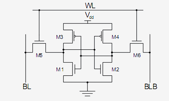
The standard way to implement one-bit SRAM is the 6-transistor circuit shown below. The topmost signal labeled WL ( Word Line ) is the address, and when it is on, the data stored in this 1-bit cell is transferred to the Bit Line , labeled BL. The output of BLB is called Bit Line Bar ; it's just the inverse of the Bit Line value. You have to learn two types of transistors and understand that M3 with M1, like M4 with M2, form an inverter.
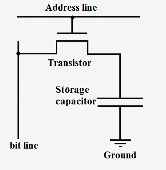
SRAM is used to build ultra-fast caches and registers inside processors. This memory is very stable, but it requires six to eight transistors to store each bit of data. Therefore, compared to DRAM, it is extremely costly in terms of cost, complexity and area on a chip. Dynamic RAM, on the other hand, stores data in a tiny capacitor, rather than using logic elements. It is called dynamic, because the voltage across a capacitor can vary significantly, since it is not connected to power or ground. There is only one transistor used to access data stored in a capacitor.
Since DRAM requires only one transistor per bit and is very scalable, it can be packed tightly and cheaply. The disadvantage of DRAM is that the capacitor charge is so small that it needs to be constantly updated. That is why after powering off the computer, all capacitors are discharged and data in RAM is lost.
Companies such as Intel, AMD and Nvidia do not publish the circuits of their processors, so it is impossible to show such complete electrical circuits for modern processors. However, this simple adder will allow you to get an idea that even the most complex parts of the processor can be divided into logical and storage elements, and then into transistors.
Now that we know how some processor components are made, we need to figure out how to put everything together and synchronize. All key components of the processor are connected to the clock signal (clock signal) . It alternately has high and low voltage, changing it with a given interval, called the frequency (frequency) . The logic inside the processor usually switches the values and performs calculations when the clock signal changes the voltage from low to high. By synchronizing all the parts, we can guarantee that the data always comes in at the right time so that there are no glitches in the processor.
You may have heard that to improve processor performance, you can increase the frequency of the clock signals. This increase in performance is due to the fact that the switching of transistors and logic inside the processor begins to occur more often than it is provided for. Since there are more cycles per second, more work can be done and the processor will have improved performance. However, this is true to a certain limit. Modern processors usually operate at a frequency of 3.0 GHz to 4.5 GHz, and this value has hardly changed in the last ten years. Just as a metal chain is no stronger than its weakest link, the processor can run no faster than its slowest part. By the end of each clock cycle, each processor element must complete its work. If some parts have not yet completed it, then the clock signal is too fast and the processor will not work. Designers call this the slowest part the critical path (Critical Path) and it determines the maximum frequency with which the processor can operate. Above a certain frequency, the transistors simply do not have enough time to switch quickly and start to fail or give the wrong output values.
By increasing the voltage of the processor, we can speed up the switching of transistors, but this also works to a certain limit. If you apply too much voltage, then we risk burning the processor. When we increase the frequency or voltage of the processor, it always starts to emit more heat and consume more power. This happens because the processor power is directly proportional to the frequency and proportional to the square of the voltage. To determine the power consumption of the processor, we consider each transistor as a small capacitor that needs to be charged or discharged as its value changes.
Powering is such an important part of the processor that in some cases up to half of the physical contacts on the chip can only be used for power or grounding. Some chips at full load can consume more than 150 amps, and with all this current you need to be controlled extremely carefully. For comparison: the central processor generates more heat per unit area than a nuclear reactor.
The clock signal in modern processors takes about 30-40% of its total power, because it is very complex and must control many different devices. To conserve power, most low-power processors shut off parts of the chip when not in use. This can be done by turning off the clock (this method is called Clock Gating) or turning off the power (Power Gating).
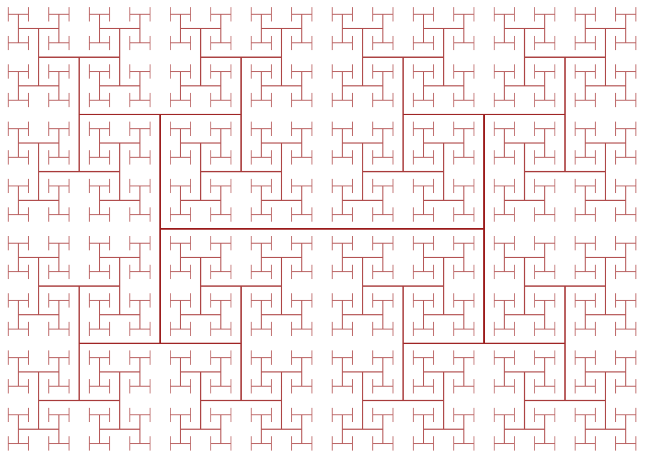
Clock signals create another difficulty when designing a processor: since their frequencies are constantly increasing, the laws of physics begin to influence the work. Even despite the extremely high speed of light, it is not large enough for high-performance processors. If you connect a clock signal to one end of the chip, then by the time the signal reaches the other end, it will be unsynchronized by a significant amount. To synchronize all parts of the chip, the clock signal is distributed using the so-called H-Tree. This is a structure that ensures that all endpoints are at exactly the same distance from the center.
It may seem that designing each individual transistor, a clock signal and a power supply pin in a chip is an extremely monotonous and complex task, and this is indeed the case. Even though companies such as Intel, Qualcomm and AMD employ thousands of engineers, they would not be able to manually design every aspect of the chip. For designing chips of this scale, they use a variety of complex tools that automatically generate structures and electrical circuits. Such tools usually receive a high-level description of what the component should do, and determine the best hardware configuration that meets these requirements. Recently, there was a development direction called High Level Synthesis , which allows developers to specify the necessary functionality in the code, after which computers determine how best to achieve it in hardware.
In the same way as you can describe computer programs through code, designers can code hardware devices. Languages such as Verilog and VHDL allow equipment designers to express the functionality of any electrical circuit they create. After performing simulations and verifying such projects, they can be synthesized into specific transistors, of which the electrical circuit will consist. Although the verification phase may not seem as exciting as designing a new cache or kernel, it is much more important than them. For each design engineer hired by the company, there may be five or more verification engineers.
Verification of a new project often takes more time and money than creating the chip itself. Companies spend so much time and money on verification, because after sending the chip into production it cannot be fixed. In case of an error in the software, you can release a patch, but the equipment works differently. For example, Intel discovered a bug in the floating-point division module of some Pentium chips, and as a result, this resulted in losses equivalent to the current $ 2 billion.
It is difficult to comprehend that there can be several billion transistors in one chip and understand what they all do. If you break the chip into its individual internal components, it becomes a bit easier. Logic elements are made up of transistors, logic elements are combined into functional modules that perform a specific task, and these functional modules are connected together to form the computer architecture, which we discussed in the first part of the series.
Most of the design work is automated, but the above allows us to realize how complex the new CPU we just bought.
In the second part of the series, I talked about the CPU design process. We discussed transistors, logic elements, power supply and synchronization signals, design synthesis and verification. In the third part, we learn what is required for the physical production of the chip. All companies love to brag about how modern their manufacturing process is (Intel is 10 nanometers, Apple and AMD are 7 nanometers, etc.), but what do these numbers really mean? We will tell about it in the following part.
Recommended reading
Source: https://habr.com/ru/post/457178/
All Articles