Tuning vias of printed circuit boards
Let's talk about the design of vias - for serious electronics, their quality is very important. At the beginning of the article I highlighted the factors affecting the integrity of the signal, and then showed examples of calculating and tuning the impedance of single and differential vias.
Hello everyone, my name is Vyacheslav. I have been working on the development of printed circuit boards for 5 years, and during this time I have not only read many rules and recommendations for tracing, but I also found primary sources and worked with them.
In complex computing systems developed by YADRO, high-speed signals on the way from the transmitter to the receiver travel considerable distances, passing through several boards and making a dozen interlayer transitions. In such conditions, each carelessly designed vias will make a small contribution to signal degradation, and as a result, the interface may not work.
')
The vias (hereinafter referred to as p / o, eng. Via) represent irregularities in the transmission line. Like other discontinuities, they spoil the signal. This effect is poorly pronounced at low frequencies, but it increases significantly with increasing frequency. Often, developers undeservedly pay little attention to the structure of vias: they can be copied from a “neighboring” project, taken from a datasheet, or not specified in the CAD system (default setting).
Before using the calculated structure, it is necessary to understand why it was made exactly like this? Blind repetition can only harm.
The integrity of the signal in the channel as it passes through the vias is mainly influenced by the following factors:
Let us consider in more detail the causes of these effects and methods for their elimination.
In a perfectly designed board, the characteristic impedance does not change throughout the course, including when moving to another layer. In reality, it usually looks like this:
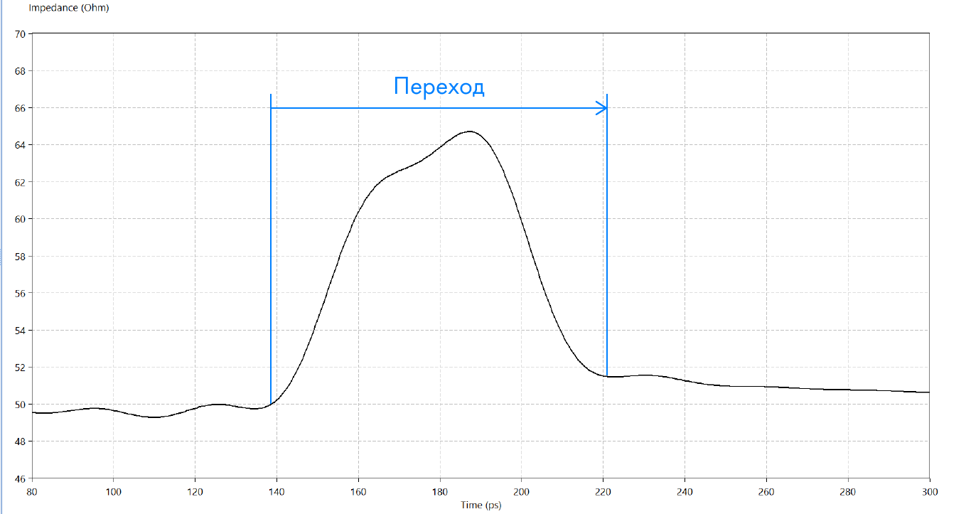
Figure 1. The change in wave resistance when moving to another layer.
The better the wave impedances are matched, the less signal will be reflected. How to affect this?
Consider the structure n / o on the board [1].

Figure 2. The structure of the p / o on the board.
By changing the elements of the n / a, we change the wave impedance of the transition. Our goal is to match the impedance of the transition structure with the impedance of the conductors to minimize reflections. Consider how the impedance changes when the elements of the p / o structure change.
Conductors on a printed circuit board can be made with a characteristic impedance that lies in a wide range, but most often it is 50 ohms. On the one hand, this is due to historical continuity: the impedance of 50 ohms has been standardized for coaxial cables as a compromise between the load level of the driver and the loss of signal energy. On the other hand, a 50-ohm conductor is easy to manufacture on a sample board.
For the developer, it is not so much the specific value of the wave resistance that is important as its constancy throughout the transmission line.
In order to make a transmission line with a fixed value of wave resistance, the developer selects the width of the track and the distance to the support layer, i.e. changes the linear capacitance and inductance of the transmission line to a certain value.
In p / o the inductive component is quite significant. In the first approximation, we must, within reason, minimize the parasitic inductance as much as possible, and then change the p / o parameters to achieve a given capacitance, and, accordingly, impedance.
An excessive decrease in the capacitance of the s / o will cause a local increase in the impedance and, as a result, signal reflections.
What happens when a signal passes through a vias with a stub?

Figure 3. A transition hole with a stub, resonance at ¼ wavelength.
In our example, the signal propagates downwards from the Top layer. Reaching the inner signal layer, the signal separates: the part moves along the route on the inner layer, and the part continues to move down the vias, then is reflected from the Bottom layer. After the reflected signal has reached the inner layer, it is again divided, a part moves along the path, and a part returns to the source.
The reflected signal will be summed up with the original one and distort it, which will be expressed in narrowing the window in the eye diagram and increasing the level of insertion loss (eng. Insertion Loss).
In the worst case, the TD segment will be equal to ¼ of the wavelength of the signal, then the reflected signal will reach the path on the inner layer with a delay of half the period, superimposed on the original signal in antiphase.
When analyzing integrity, it is recommended to consider the bandwidth of 5 Nyquist frequencies. A good approximation would be considered acceptable stab, which gives resonance at 7 harmonics and above [2].
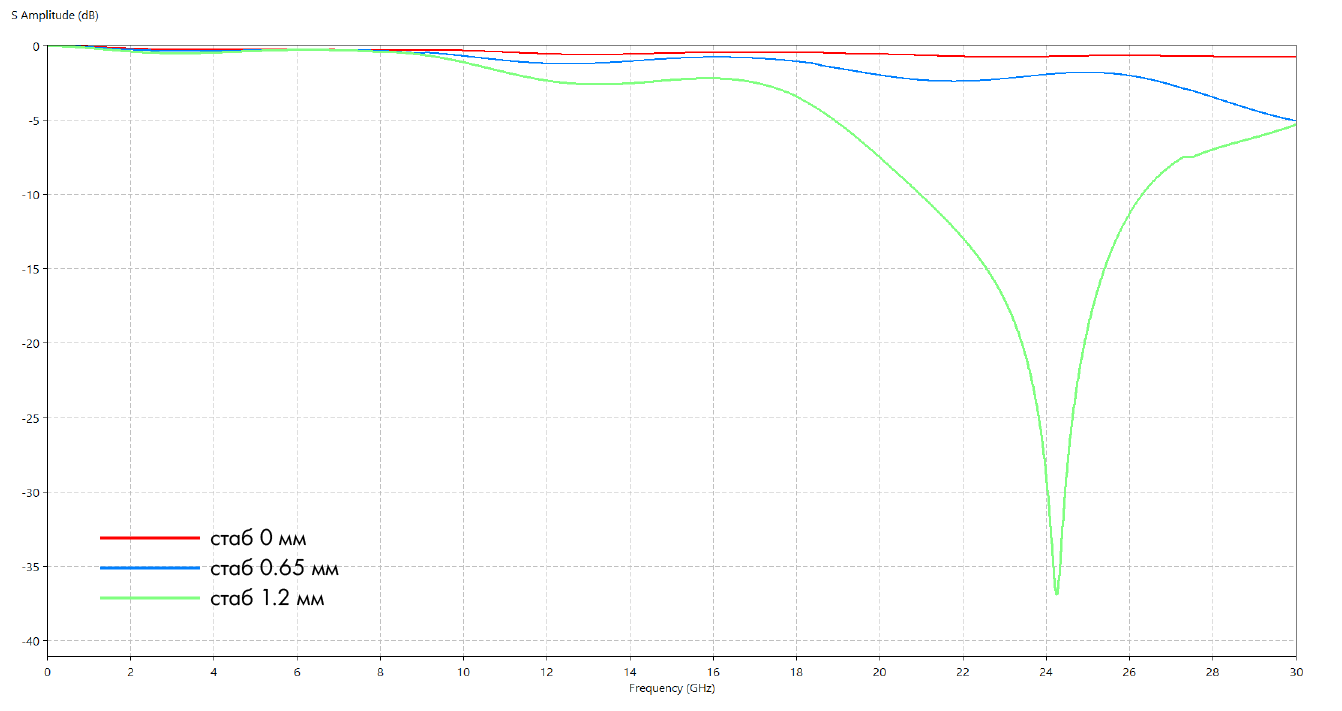
Figure 4. Graph of the level of insertion loss for p / o with stubs 0, 0.65, 1.2 mm.
Figure 4 shows a huge resonance at frequencies around 24 GHz. We can conclude that if our signal operates at a frequency of 2-3 GHz, we can afford not to eliminate the stub, because within 7 harmonics “everything is calm”.
A quick assessment of the stub criticality can be made in the Polar calculator :


Figure 5. Image from polarinstruments.com . A stub length of 2.5 mm is permissible for signals with a rise time of more than 500 ps.
A slightly more accurate result is given by the formulas given in the article [2]. They take into account the p / o geometry and allow us to calculate the correction for the dielectric constant of the dielectric along the Z axis.
Eliminate the stub by using the operation "reverse drilling" (eng. Backdrilling), or using microtransitions (eng. Blind and buried vias). The choice depends on the features of the project. Reverse drilling is easier and cheaper. After the board is manufactured, a stub drill of larger diameter is drilled to a predetermined depth. The developer is required to set additional indentations of the topology in the drilling zone, and it is also available for the manufacturer to indicate the drilling requirements in the design documentation. Modern CAD systems support this functionality.
Microtransitions are primarily intended for high density boards (HDI), but in some cases they can be used by leveling out the high cost of failure by reverse drilling and reducing the number of layers on the board. When developing HDI boards, you should remember some features:
It is highly recommended to agree on the board structure with the manufacturer in advance.
Cross-talk - unwanted signal transmission from one line to the next. This transmission occurs because two closely spaced conductors have capacitive and inductive coupling.
The nature of the crosstalk signal wires and p / o is slightly different.
In the s / c signal has no support layer, the return currents flow along the adjacent s / v, forming a large loop. Cross-interference signals in the p / o due to the inductive component.
The greatest effect on minimizing crosstalk can be achieved by increasing the distance between the n / a. However, the topologist often does not have much space.
The convergence of the p / o in a differential pair not only reduces the occupied area, but also has a positive effect on noise immunity [3].
The generally accepted way to minimize crosstalk between adjacent signal p / o - put a screening p / o between them. With this method, you will need to drive signals with a pitch of about 2 mm (Figure 6). If there is not enough space, you can use a smaller step with a shift (eng. Staggered pattern), as in Figure 7. Using simulation, you can choose the ideal angle of shift [4].
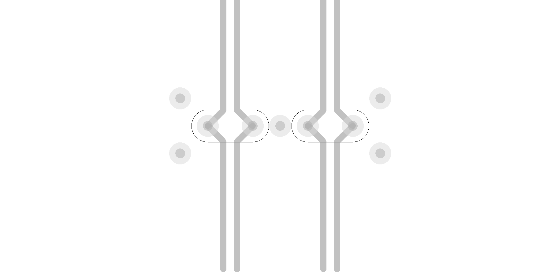
Figure 6. Minimizing cross-talk with shielding p / o.
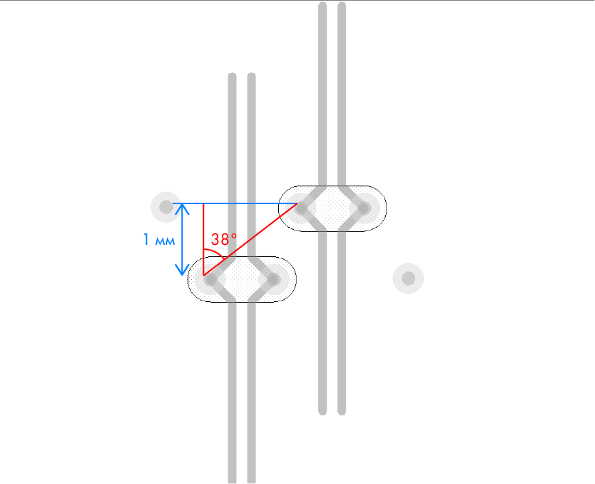
Figure 7. Minimizing crosstalk using a diagonal “chess” shift.
Cross-talk can also be reduced by exotic methods, for example, a long stub (due to the shift of the inductive-capacitive balance of the n / a) [5]. Also, noise can be reduced at the design stage of the microcircuit case [6].
In addition to adjacent signal circuits, signal quality can be interfered with by the inner layers.
On the polygons of power can flow large currents. Due to the increase in inductance at the edges of the polygons, the flowing currents form the marginal fields (Fringing fields) along all the boundaries of the polygon, including the cutouts. Edge fields are a source of electromagnetic radiation (English Edge-fired emission) in space. To reduce the emission of electromagnetic radiation, rule 20H is applied (Figure 8), which consists in narrowing the power range to the land range.
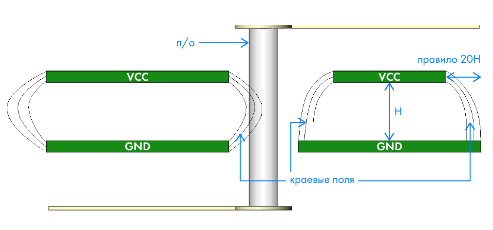
Figure 8. Edge margins and rule 20H.
To protect the p / o from interference, if possible, it is necessary to increase the anti-drop on the power supply grounds. The 20H rule for semiconductor is difficult to provide, and indeed, it is usually recommended to have an anti-drop about 2 mm in diameter (Figure 9).

Figure 9. Increased anti-drop on power layers
Based on knowledge of the effect of p / o elements on impedance, we can design our ideal p / o. An excellent start will be the calculation of the impedance in the calculator.
Calculators such as Saturn PCB Design Toolkit and Polar Instruments Si9000e are popular with PCB development engineers . Both of them allow you to quickly calculate the impedance of a single p / o.
The result obtained in these calculators is very different from each other. This is due to the fact that these tools have a different approach.
Polar counts impedance in a two-dimensional plane, where n / o crosses the power range. The calculation formula is not given. It was established experimentally that the calculation is made according to the impedance formula of a coaxial cable:

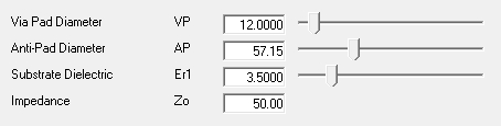
Figure 10. Image from polarinstruments.com
The illustration shows a rather low value of the dielectric constant Er1, compared with the standard. This is due to the heterogeneity of the structure of the dielectric: it consists of resin (Er 3.2) and fiberglass filaments (Er 6.1), therefore it has an average dielectric constant of about 4.1. This value can vary quite locally. So, near p / o resin predominates, therefore, the value of dielectric constant is recalculated in the direction of decreasing [7].
Saturn PCB considers impedance using the formula:
When changing the length p / o, the values of inductance and capacitance change disproportionately, the impedance changes. The impedance of exactly the same p / o long 1.6 mm, Saturn PCB counts as 128 Ohms! (Figure 11)

Figure 11. The calculation of the p / o in the Saturn PCB Design Toolkit.
Immediately the question arises: who to believe?
We will model in a three-dimensional electromagnetic field solver (the 3D Solver), as it will look on a real 8-layer board with a thickness of 1.6 mm (Figure 12)
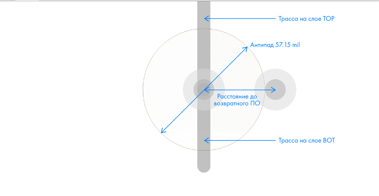
Figure 12. Structure of the transition between layers with a hole for the return current.
In our case, the impedance was about 70 ohms. By bringing the return p / o closer, you can reduce it by another 5 ohms. By “playing” with the size of the anti-attack, you can quite accurately adjust the impedance to the target value (Figure 13).
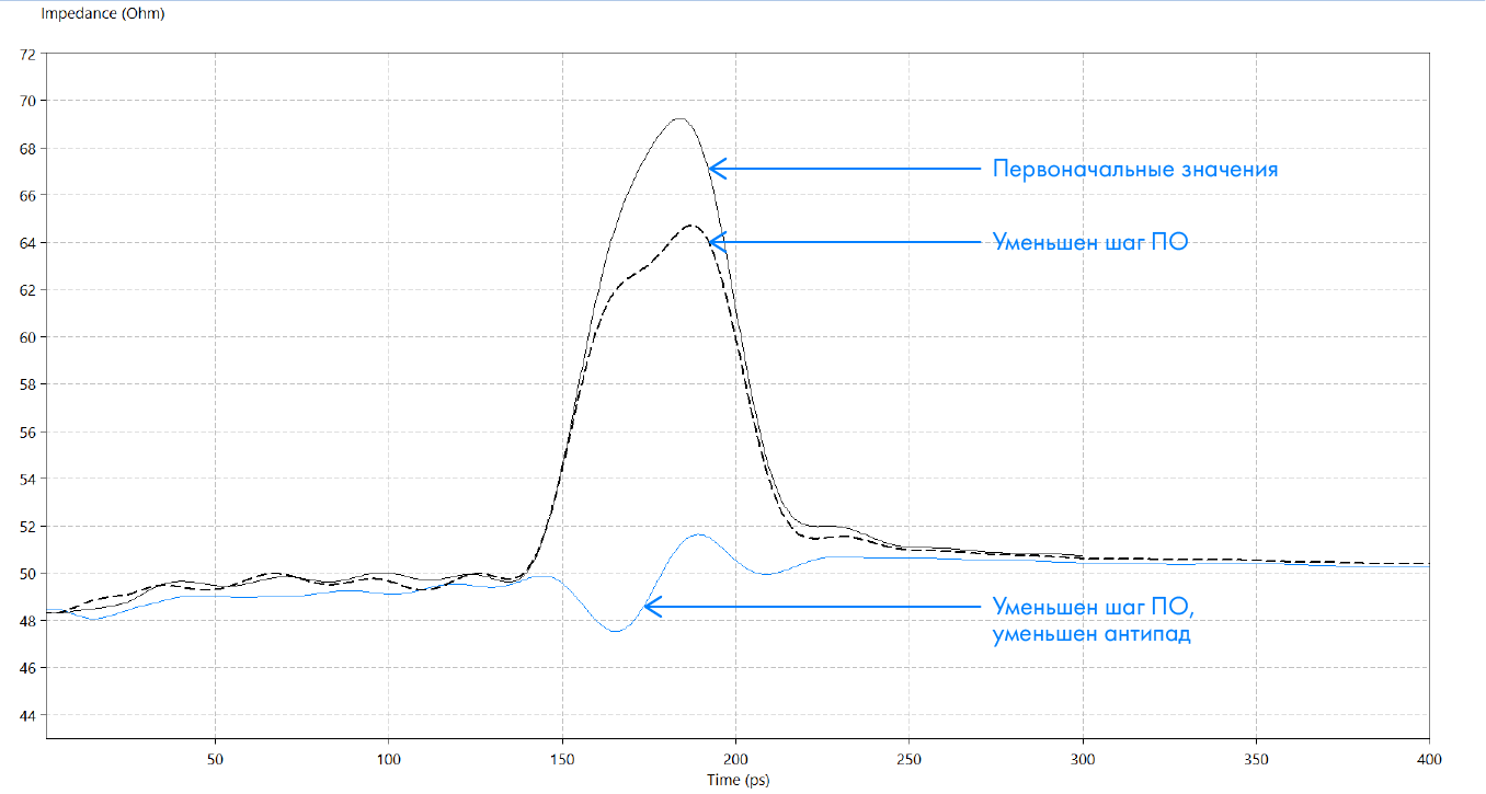
Figure 13. The impedance of the circuit with p / o on the timing diagram.
In the frequency domain, the “best” parameters are expressed in a smaller value of the reflection coefficient from the input (Figure 14).
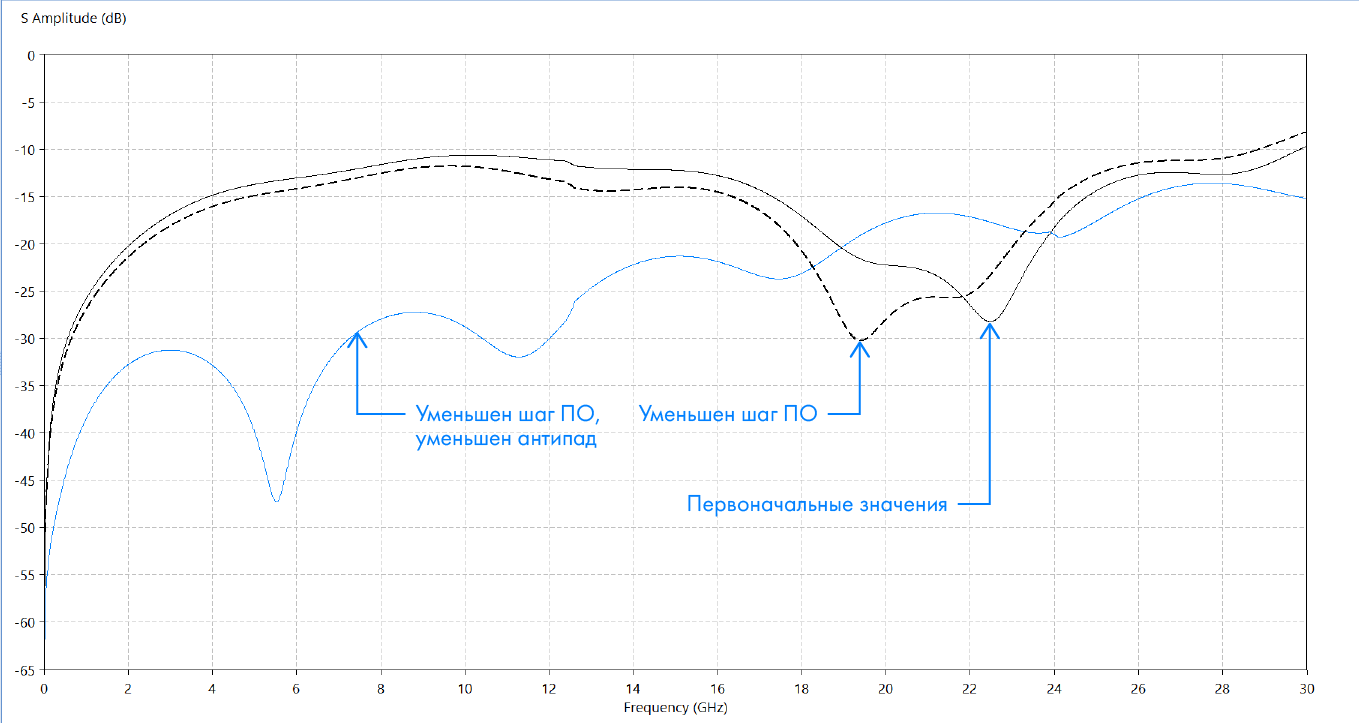
Figure 14. Parameters of single p / o in the frequency domain.
Polar calculation was closer to the result. It is possible that in order to get an adequate result in Saturn PCB, corrections are required. If someone has a positive experience with impedance calculation in Saturn, share in the comments!
The calculation of differential p / o is similar to single, except that now we do not have a calculator: the above tools do not consider differential p / o. Also, now we can additionally change the p / o step in the diff. a pair.
We take the same structure: an 8-layer board with a thickness of 1.6 mm. Consider the 9 p / o configurations (Figure 15).
The first 3 p / o have gaps of 0.125 mm and differ only in the location of the holes for the return current. All n / a c 4 and further have a pitch of 1 mm. P / o c 6 and further have an increased anti-drop (0.250 mm) and are distinguished by the indentation of the holes for the return current.
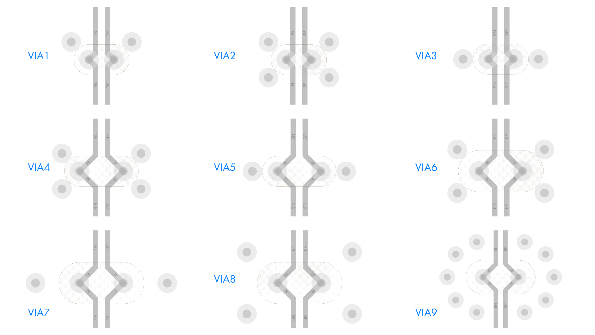
Figure 15. Bores.
Consider the impedance plot (Figure 16).
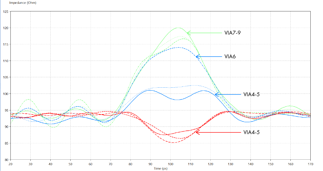
Figure 16. Impedance p / o in the time domain.
The “hump” is clearly visible on the chart, which corresponds to the vertical segment of the p / o - “glass” (eng. Via barrel).
Considering the frequency dependence of the reflection coefficient VIA1-3 (Figure 17), we see that despite the good performance at the target frequency of 6 GHz, there is a resonance at lower frequencies. It is preferable to improve via7-9, and if it does not work out, then via4-5, to reduce the "hump" due to the shift of the graphs to the right.

Figure 17. Reflection coefficient from the input p / o.
Reduce the anti-drop in VIA9 to get gaps of 0.125 mm. For VIA4, reduce the p / o step to 0.75 mm and consider the result obtained (Figure 18).

Figure 18. Comparison of impedance modified p / o.
In the frequency domain, the shift of the reflection coefficient graph from the input to the right is seen (Figure 19).

Figure 19. Comparison of reflection coefficient of modified p / o.
Vents in PCBs are complex and non-uniform structures. To correctly calculate the parameters, expensive 3D solvers, competencies and time consuming are required.
If it is not possible to avoid the use of transitions of critical signals to other layers, it is necessary first of all to assess the degree of influence of inhomogeneities on the integrity of signals. If the inhomogeneity is electrically short (the delay time is less than 1/6 of the front), the stub resonates at frequencies outside the passband - it makes no sense to spend time and money on optimization.
In the first approximation, it is convenient to use ready-made structures from datasheets or previous boards, but remember the features of the current project.
Calculators allow you to quickly assess the parameters of the p / o, however, they use strongly simplified models that adversely affect the result.
Hello everyone, my name is Vyacheslav. I have been working on the development of printed circuit boards for 5 years, and during this time I have not only read many rules and recommendations for tracing, but I also found primary sources and worked with them.
In complex computing systems developed by YADRO, high-speed signals on the way from the transmitter to the receiver travel considerable distances, passing through several boards and making a dozen interlayer transitions. In such conditions, each carelessly designed vias will make a small contribution to signal degradation, and as a result, the interface may not work.
')
Signal integrity
The vias (hereinafter referred to as p / o, eng. Via) represent irregularities in the transmission line. Like other discontinuities, they spoil the signal. This effect is poorly pronounced at low frequencies, but it increases significantly with increasing frequency. Often, developers undeservedly pay little attention to the structure of vias: they can be copied from a “neighboring” project, taken from a datasheet, or not specified in the CAD system (default setting).
Before using the calculated structure, it is necessary to understand why it was made exactly like this? Blind repetition can only harm.
The integrity of the signal in the channel as it passes through the vias is mainly influenced by the following factors:
- signal reflection due to changes in wave resistance;
- signal degradation due to parasitic capacitance and inductance;
- reflections from an unused piece of p / o during the transition to the inner layer (hereinafter, the stub from the English via stub);
- crosstalk (English Cross talks);
- interference in power tires.
Let us consider in more detail the causes of these effects and methods for their elimination.
Factor 1. Wave resistance p / o
In a perfectly designed board, the characteristic impedance does not change throughout the course, including when moving to another layer. In reality, it usually looks like this:
Figure 1. The change in wave resistance when moving to another layer.
The better the wave impedances are matched, the less signal will be reflected. How to affect this?
Consider the structure n / o on the board [1].
Figure 2. The structure of the p / o on the board.
| Layer | Element | Property |
|---|---|---|
| TOP | Playground | Parasitic capacitance between the platform and the L2 power ground |
| TOP-L2 | segment p / o | Inductance |
| L2 (food landfill) | Antipad | The anti-drop forms the edge capacity - the capacity between the walls of the p / o and the power range. |
| L2-L3 | Cut p / o | Inductance |
| L3 (food ground) | Antipad | The anti-drop forms the edge capacity - the capacity between the walls of the p / o and the power range. |
| L3-L4 | Cut p / o | Inductance |
| L4 (signal) | Playground | Parasitic capacitance between the p / o site and the L3 power supply ground |
| L4-L5 | Stub | Noise source |
By changing the elements of the n / a, we change the wave impedance of the transition. Our goal is to match the impedance of the transition structure with the impedance of the conductors to minimize reflections. Consider how the impedance changes when the elements of the p / o structure change.
| Element | Act | Electrical property | Impedance (result) |
|---|---|---|---|
| Playground | ↓ | C ↓ | ↑ |
| Diameter n / a | ↓ | L ↑ | ↑ |
| Antipad | ↑ | C ↓ | ↑ |
| P / o length | ↑ | L ↑ | ↑ |
| The number of food polygons on the way p / o | ↓ | C ↓ | ↑ |
| Step p / o | ↑ | C ↓ | ↑ |
| Distance to return p / o | ↑ | L ↑ | ↑ |
| Number of return p / o | ↑ | L ↓ | ↓ |
| Filling holes | Fill with resin (Dk ↑) | With ↑ | ↓ |
Factor 2. Parasitic inductance and capacitance
Conductors on a printed circuit board can be made with a characteristic impedance that lies in a wide range, but most often it is 50 ohms. On the one hand, this is due to historical continuity: the impedance of 50 ohms has been standardized for coaxial cables as a compromise between the load level of the driver and the loss of signal energy. On the other hand, a 50-ohm conductor is easy to manufacture on a sample board.
For the developer, it is not so much the specific value of the wave resistance that is important as its constancy throughout the transmission line.
In order to make a transmission line with a fixed value of wave resistance, the developer selects the width of the track and the distance to the support layer, i.e. changes the linear capacitance and inductance of the transmission line to a certain value.
In p / o the inductive component is quite significant. In the first approximation, we must, within reason, minimize the parasitic inductance as much as possible, and then change the p / o parameters to achieve a given capacitance, and, accordingly, impedance.
An excessive decrease in the capacitance of the s / o will cause a local increase in the impedance and, as a result, signal reflections.
Factor 3. Via stub
What happens when a signal passes through a vias with a stub?
Figure 3. A transition hole with a stub, resonance at ¼ wavelength.
In our example, the signal propagates downwards from the Top layer. Reaching the inner signal layer, the signal separates: the part moves along the route on the inner layer, and the part continues to move down the vias, then is reflected from the Bottom layer. After the reflected signal has reached the inner layer, it is again divided, a part moves along the path, and a part returns to the source.
The reflected signal will be summed up with the original one and distort it, which will be expressed in narrowing the window in the eye diagram and increasing the level of insertion loss (eng. Insertion Loss).
In the worst case, the TD segment will be equal to ¼ of the wavelength of the signal, then the reflected signal will reach the path on the inner layer with a delay of half the period, superimposed on the original signal in antiphase.
When analyzing integrity, it is recommended to consider the bandwidth of 5 Nyquist frequencies. A good approximation would be considered acceptable stab, which gives resonance at 7 harmonics and above [2].
Figure 4. Graph of the level of insertion loss for p / o with stubs 0, 0.65, 1.2 mm.
Figure 4 shows a huge resonance at frequencies around 24 GHz. We can conclude that if our signal operates at a frequency of 2-3 GHz, we can afford not to eliminate the stub, because within 7 harmonics “everything is calm”.
A quick assessment of the stub criticality can be made in the Polar calculator :
Figure 5. Image from polarinstruments.com . A stub length of 2.5 mm is permissible for signals with a rise time of more than 500 ps.
A slightly more accurate result is given by the formulas given in the article [2]. They take into account the p / o geometry and allow us to calculate the correction for the dielectric constant of the dielectric along the Z axis.
Eliminate the stub by using the operation "reverse drilling" (eng. Backdrilling), or using microtransitions (eng. Blind and buried vias). The choice depends on the features of the project. Reverse drilling is easier and cheaper. After the board is manufactured, a stub drill of larger diameter is drilled to a predetermined depth. The developer is required to set additional indentations of the topology in the drilling zone, and it is also available for the manufacturer to indicate the drilling requirements in the design documentation. Modern CAD systems support this functionality.
Microtransitions are primarily intended for high density boards (HDI), but in some cases they can be used by leveling out the high cost of failure by reverse drilling and reducing the number of layers on the board. When developing HDI boards, you should remember some features:
- each new type of payment order increases the cost of the board;
- for laser drilling, special optimized prepregs are used, whose properties may differ;
- metallization of blind holes increases the thickness of the copper on the inner layers.
It is highly recommended to agree on the board structure with the manufacturer in advance.
Factor 4. Cross-talk
Cross-talk - unwanted signal transmission from one line to the next. This transmission occurs because two closely spaced conductors have capacitive and inductive coupling.
The nature of the crosstalk signal wires and p / o is slightly different.
In the s / c signal has no support layer, the return currents flow along the adjacent s / v, forming a large loop. Cross-interference signals in the p / o due to the inductive component.
The greatest effect on minimizing crosstalk can be achieved by increasing the distance between the n / a. However, the topologist often does not have much space.
The convergence of the p / o in a differential pair not only reduces the occupied area, but also has a positive effect on noise immunity [3].
The generally accepted way to minimize crosstalk between adjacent signal p / o - put a screening p / o between them. With this method, you will need to drive signals with a pitch of about 2 mm (Figure 6). If there is not enough space, you can use a smaller step with a shift (eng. Staggered pattern), as in Figure 7. Using simulation, you can choose the ideal angle of shift [4].
Figure 6. Minimizing cross-talk with shielding p / o.
Figure 7. Minimizing crosstalk using a diagonal “chess” shift.
Cross-talk can also be reduced by exotic methods, for example, a long stub (due to the shift of the inductive-capacitive balance of the n / a) [5]. Also, noise can be reduced at the design stage of the microcircuit case [6].
Factor 5. Tire Power Disturbance
In addition to adjacent signal circuits, signal quality can be interfered with by the inner layers.
On the polygons of power can flow large currents. Due to the increase in inductance at the edges of the polygons, the flowing currents form the marginal fields (Fringing fields) along all the boundaries of the polygon, including the cutouts. Edge fields are a source of electromagnetic radiation (English Edge-fired emission) in space. To reduce the emission of electromagnetic radiation, rule 20H is applied (Figure 8), which consists in narrowing the power range to the land range.
Figure 8. Edge margins and rule 20H.
To protect the p / o from interference, if possible, it is necessary to increase the anti-drop on the power supply grounds. The 20H rule for semiconductor is difficult to provide, and indeed, it is usually recommended to have an anti-drop about 2 mm in diameter (Figure 9).
Figure 9. Increased anti-drop on power layers
Single impedance impedance calculation
Based on knowledge of the effect of p / o elements on impedance, we can design our ideal p / o. An excellent start will be the calculation of the impedance in the calculator.
Calculators such as Saturn PCB Design Toolkit and Polar Instruments Si9000e are popular with PCB development engineers . Both of them allow you to quickly calculate the impedance of a single p / o.
The result obtained in these calculators is very different from each other. This is due to the fact that these tools have a different approach.
Polar counts impedance in a two-dimensional plane, where n / o crosses the power range. The calculation formula is not given. It was established experimentally that the calculation is made according to the impedance formula of a coaxial cable:
Figure 10. Image from polarinstruments.com
The illustration shows a rather low value of the dielectric constant Er1, compared with the standard. This is due to the heterogeneity of the structure of the dielectric: it consists of resin (Er 3.2) and fiberglass filaments (Er 6.1), therefore it has an average dielectric constant of about 4.1. This value can vary quite locally. So, near p / o resin predominates, therefore, the value of dielectric constant is recalculated in the direction of decreasing [7].
Saturn PCB considers impedance using the formula:
When changing the length p / o, the values of inductance and capacitance change disproportionately, the impedance changes. The impedance of exactly the same p / o long 1.6 mm, Saturn PCB counts as 128 Ohms! (Figure 11)
Figure 11. The calculation of the p / o in the Saturn PCB Design Toolkit.
Immediately the question arises: who to believe?
We will model in a three-dimensional electromagnetic field solver (the 3D Solver), as it will look on a real 8-layer board with a thickness of 1.6 mm (Figure 12)
Figure 12. Structure of the transition between layers with a hole for the return current.
In our case, the impedance was about 70 ohms. By bringing the return p / o closer, you can reduce it by another 5 ohms. By “playing” with the size of the anti-attack, you can quite accurately adjust the impedance to the target value (Figure 13).
Figure 13. The impedance of the circuit with p / o on the timing diagram.
In the frequency domain, the “best” parameters are expressed in a smaller value of the reflection coefficient from the input (Figure 14).
Figure 14. Parameters of single p / o in the frequency domain.
Polar calculation was closer to the result. It is possible that in order to get an adequate result in Saturn PCB, corrections are required. If someone has a positive experience with impedance calculation in Saturn, share in the comments!
Impedance calculation of differential vias
The calculation of differential p / o is similar to single, except that now we do not have a calculator: the above tools do not consider differential p / o. Also, now we can additionally change the p / o step in the diff. a pair.
We take the same structure: an 8-layer board with a thickness of 1.6 mm. Consider the 9 p / o configurations (Figure 15).
The first 3 p / o have gaps of 0.125 mm and differ only in the location of the holes for the return current. All n / a c 4 and further have a pitch of 1 mm. P / o c 6 and further have an increased anti-drop (0.250 mm) and are distinguished by the indentation of the holes for the return current.
Figure 15. Bores.
Consider the impedance plot (Figure 16).
Figure 16. Impedance p / o in the time domain.
The “hump” is clearly visible on the chart, which corresponds to the vertical segment of the p / o - “glass” (eng. Via barrel).
Considering the frequency dependence of the reflection coefficient VIA1-3 (Figure 17), we see that despite the good performance at the target frequency of 6 GHz, there is a resonance at lower frequencies. It is preferable to improve via7-9, and if it does not work out, then via4-5, to reduce the "hump" due to the shift of the graphs to the right.
Figure 17. Reflection coefficient from the input p / o.
Reduce the anti-drop in VIA9 to get gaps of 0.125 mm. For VIA4, reduce the p / o step to 0.75 mm and consider the result obtained (Figure 18).
Figure 18. Comparison of impedance modified p / o.
In the frequency domain, the shift of the reflection coefficient graph from the input to the right is seen (Figure 19).
Figure 19. Comparison of reflection coefficient of modified p / o.
Final Recommendations
Vents in PCBs are complex and non-uniform structures. To correctly calculate the parameters, expensive 3D solvers, competencies and time consuming are required.
If it is not possible to avoid the use of transitions of critical signals to other layers, it is necessary first of all to assess the degree of influence of inhomogeneities on the integrity of signals. If the inhomogeneity is electrically short (the delay time is less than 1/6 of the front), the stub resonates at frequencies outside the passband - it makes no sense to spend time and money on optimization.
In the first approximation, it is convenient to use ready-made structures from datasheets or previous boards, but remember the features of the current project.
Calculators allow you to quickly assess the parameters of the p / o, however, they use strongly simplified models that adversely affect the result.
Bibliography
- Chin, T. Differential pairs: four things you need to know about vias. Retrieved from TI E2E Community: https://e2e.ti.com/blogs_/b/analogwire/archive/2015/06/10/differential-pairs-four-things-you-need-to-know-about-vias#
- Simonovich, B. Via Stubs Demystified. Retrieved from Bert Simonovich's Design Notes: https://blog.lamsimenterprises.com/2017/03/08/via-stubs-demystified/
- Demystifying Vias in High-Speed PCB Design. Retrieved from Keysight Technology: https://www.keysight.com
- K. Aihara, J. Buan, A. Nagao, T. Takada and CC Huang, “Minimizing differential transmissions,” in Proc. 14th Elect. Perform. Electron. Packages and Systems, Portland, OR, Oct. 2014
- CM Nieh and J. Park, “Far-End Crosstalk Cancellation using the DDR4 Memory Channel,” in Proc. 63rd Electronics Components and Technology Conference, Las Vegas, NV, May 2013, pp. 2035-2040.
- H. Kanno, H. Ogura, and K. Takahashi, “Surface Transition Compensating Wireline V-band, Included with V-band,” in IEEE MTT-S Int. Microwave Symp. Dig., Philadelphia, PA, June 2003, pp. 1159-1162.
- Via Pad / Anti-Pad Impedance Calculation. Retrieved from Polar instruments https://www.polarinstruments.com/support/si/AP8178.html
Source: https://habr.com/ru/post/456828/
All Articles