Microelectronics technology on the fingers: "Moore's law", marketing moves, and why nanometers are not the same today. Part 2
In the first part, we covered briefly the physics of silicon, microelectronics technology, and technological limitations. Now let's talk about the physical limitations and physical effects that affect the size of the elements in the transistor. There are many of them, so let's go through the main ones. Here you will have to get into physics, otherwise nothing.
Disclaimer: Once upon a time I also dabbled in writing articles about making chips , and in the “Inside Look” series of articles I even looked inside them, i.e. The subject is extremely interesting to me. Naturally, I would like the author of the original article to publish it on Habré, but in connection with his employment, he allowed me to transfer it here. Unfortunately, the Habr rules do not allow direct copy-paste, so I added links to sources, images and a little bit of ad-libbing and tried to straighten the text a little. Yes, I know and respect the articles ( 1 and 2 ) on this topic from amartology .
Physical effects in microelectronics
The order of the basic values for silicon
The concentration of silicon atoms in the crystal - 10 22 cm -3
The concentration of its own electrons and holes at room temperature is 10 10 cm -3
The concentration of impurity atoms from weakly doped regions - 10 16 -10 18 cm -3
The concentration of impurity atoms from heavily doped regions - 10 19 -10 20 cm -3
The concentration of impurity atoms from very heavily doped regions is 10 21 cm -3 . In this case, one already speaks of a degenerate semiconductor , since such a concentration (one impurity atom for 10 or less silicon atoms) changes the energy structure of the crystal.
')
Dependence of the characteristics of silicon on temperature
From the first part, we remember that at room temperature pure silicon is a dielectric. A pair of electron-holes occurs only in one of a trillion cases, but this fraction increases with temperature exponentially. There is such a thing - the doubling temperature of the concentration of own charge carriers. For silicon, it is about 9 degrees.
Those. we increase the temperature by 9 degrees, the percentage of decayed silicon atoms increases by 2 times; 18 degrees - 4 times; 27 degrees - 8 times; 36 degrees - 16 times; 45 - 32 times; 90 - 1024 times; 180 - 10 6 times; 270 - 10 9 times.
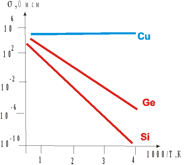
Comparison of the temperature conductivity of copper, silicon and germanium. A source
We get that when heated to 200 degrees (~ 2.1 on the graph above), the intrinsic concentration of electron-hole pairs becomes equal to 10 16 , which is equal to the impurity concentration of weakly doped layers. At 300 degrees (~ 1.75) already 10 19 , this is the concentration of heavily doped layers (n + and p +). At such a temperature, silicon actually turns into a conductor and transistors lose controllability.
Problems will begin much earlier. The temperature in the microcircuit is uneven. There are local heating zones, usually in the middle of the chip. If the temperature in some small area exceeds 200 degrees, then the leakage current starts to increase due to an increase in the intrinsic conductivity of silicon. This leads to even more heating, and this further increases the leakage current and expands the overheating area. The process becomes irreversible and ... booms. And irrevocably. Therefore, on all large circuits, an automatic overheating protection is installed.
That is why it is so important to prevent strong heating of the crystal.
For comparison, the concentration of intrinsic electrons and holes in gallium nitride at room temperature is several orders of magnitude lower, and the doubling temperature of the number of intrinsic charge carriers is about 25 degrees. The problems described above in gallium nitride start at about 600-700 degrees.
Tunnel current
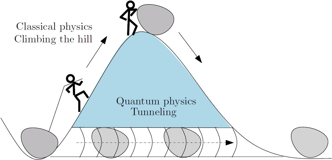
This phenomenon is both complex and simple at the same time. The roots lie in the quantum nature of the electron. The electron lives according to the laws of quantum mechanics, which is not always clear from the point of view of classical physics. According to these laws, an electron is not only a particle, but also a wave, and its behavior can be calculated only with some probability. There is such a formula Heisenberg:
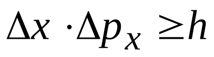
It is also called the Heisenberg uncertainty relation . From the formula it follows that the spatial parameters of the electron cannot be determined with an accuracy greater than a certain value (Planck's constant). In extreme cases of the equation, if we know the exact location of the electron, we will not know anything about its speed and direction of motion. If you know exactly the speed and direction, then nothing will be known about his whereabouts. It turns out that the electron is such a particle diffuse in space with peaks of the probability of being. At any time, an electron can be at any point of the Universe without any external influence. True, the probability of its occurrence very far from the current location is vanishingly small.
Now we will present the structure Metal - Dielectric - Semiconductor n-type (MIS). In a metal, the concentration of free electrons is approximately equal to the concentration of atoms (10 22 / cm 3 ). They cannot penetrate a dielectric, because for electrons from a metal it is an area of forbidden energies. Inside the dielectric electron-wave with energy in the metal will begin to interfere (self-destruct itself). But they can materialize in an n-type semiconductor, where for them there is a zone of allowed energies. Electrons pass from metal to semiconductor through an oxide layer without any external influence, simply by virtue of their probabilistic nature. This is the tunnel current . The process itself is called tunneling, or quantum tunneling (that sounds cooler!).
The additional energy that would have to be added to the electron for “classical” penetration into the oxide is called a potential barrier. Schematically, the electron as if gnaws a tunnel through a potential barrier.
There is a flow in the opposite direction - from the semiconductor to the metal. But since the concentration of free electrons in a semiconductor is several orders of magnitude smaller, the reverse flow is proportionally less.
The p-type semiconductor for electrons from a metal is also a forbidden energy zone. However, a reverse process is possible here — the tunneling of valence electrons from a semiconductor to a metal with the appearance of holes in silicon. It looks like these holes are tunneling from metal. The intensity, other things being equal, is about 10 times lower than the tunneling of free electrons.
Tunnel current for distances above 1 μm can be neglected. Too low probability and transitions are too rare. As the distance decreases, the probability of spontaneous transitions increases sharply. At distances of nm, the tunneling current increases by a factor of 10 with an approximation of 0.2 nm.
A similar mechanism works for npn silicon layers. For a free electron from the n-region, the p-region is a zone of forbidden energies, no transitions occur. But if the width of the p-base is set too narrow, the electrons begin to tunnel directly from the source to the drain. This limits the theoretical maximum base width to 8 nm. At smaller sizes, due to the tunneling current, the source - drain transistor becomes in principle uncontrollable.
For pnp structures, the situation is similar, but holes (valence electrons) tunnel.
In degenerate semiconductors (heavily doped) in the band of forbidden energies there are islands of allowed energies. For them, the option of tunneling on these islands. Approximately how to overcome a stream by jumping over boulders sticking out.
Space Charge Area (SCR)
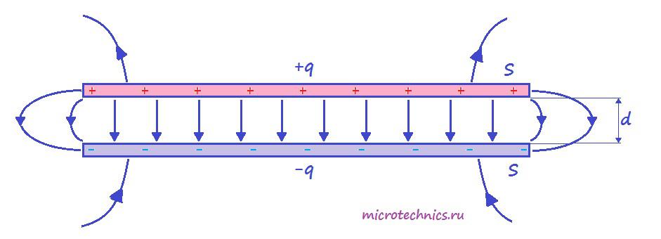
The space charge region (SCR), which is also the depleted region, it is also the space charge region, is an electrically charged layer that forms at the interface between the n- and p-regions.

Mentally connect two pieces of silicon, one n-type, the other p-type. In the n-layer there are a lot of free electrons, in the p-layer there are a lot of holes, they move chaotically. Part of the free electrons goes into the p-layer, part of the holes in the n-layer. As a result, uncompensated positive ions remain in the n-layer, and uncompensated negative ions in the p-layer. A local electric field appears along the boundary of the regions, which begins to hinder further transitions. The field strength is maximal at the boundary, and gradually decreases with distance. In the end, the field strength becomes such that the transfer of holes and electrons cease and an equilibrium state is established. For silicon, the voltage of such an internal field is about 0.5 volts. Depends on the concentration of impurities on both sides. The dependence is weak, about 0.1 volts when the concentration changes 10 times.
In addition to the appearance of an electric field at the boundary, there is a decrease in the concentration of free electrons and holes. Directly on the boundary of the layers to zero. Hence the second name - "depleted area". The width of this region depends on the voltage at the junction and the concentration of impurities. The dependence on the concentration of impurities is inverse quadratic, i.e. with an increase in concentration by 100 times, the width of the SCR decreases by a factor of 10 (in fact, slightly less, because the voltage at the transition increases).
This is the state when no external voltage is applied to the structure.
If an external voltage is applied, it is vectorially added to the internal one.

We apply a small direct voltage to the junction, i.e. plus (+) to the p-layer, minus (-) to the n-layer. The external and internal fields are directed in different directions and begin to compensate each other. The voltage at the junction and the width of the SCR decreases. When the voltage of the external field becomes higher than the internal one, the SCR disappears, the pn junction opens fully. For semiconductor diodes there is even such a parameter - the threshold voltage. This is a direct voltage at which the diode is fully open.

Now we apply the reverse voltage: minus (-) to the p-layer, plus (+) to the n-layer. The external and internal fields are added, the voltage at the junction and the width of the SCR grow.
If we translate this model to our field effect transistor, we get the picture below:
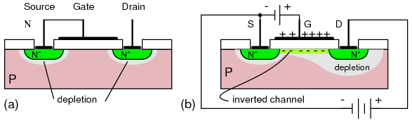
Light pink marked depleted areas (SCR). We get that the real width of the active base , which is controlled by the gate voltage, is less than the source-drain distance. That is, the size of the base minus the width of the SCR transitions. In the absence of supply voltage, the width of the SCR of the source and drain is the same. If the working voltage is applied, the width of the OPZ of the drain increases, since it is under reverse bias. The active base narrows even more:
If the base is too short, the SCR of the drain and source are connected. The width of the active base becomes equal to 0, the through current will flow from the drain to the source, the transistor opens. Regardless of the voltage at the gate. The transistor becomes unmanageable. The effect is called “base puncture”.
There is also an intermediate variant, when the SCR does not close, but the distance from the source to the boundary of the SCR of the drain is less than 8 nm. Then in the SCR begin to tunnel electrons from the source. Once in the SCR, they are transferred to the drain by an electric field. Simply put, a decent tunnel current will flow from source to drain.
Avalanche breakdown
If the intensity of the electric field inside the SCR becomes too high, then an electron accidentally flown into it accelerates so much that it takes the electron from a neutral atom. 2 electrons appear, they accelerate again and strip electrons from the next ones, etc. The process resembles an avalanche, hence the name. In the SCR appears conductive channel through which current flows. The transistor spontaneously opens.
A similar situation can occur in the gate dielectric. If the field strength is higher than the threshold, the “fast” electron that has flown from the metal accelerates and causes an avalanche.
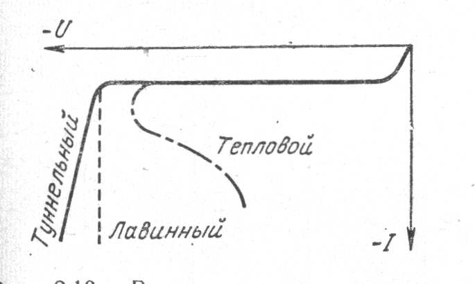
Visual comparison of different types of breakdown. A source
To avoid such avalanche breakdown, it is necessary to prevent the field strength from exceeding the breakdown value. Field strength = Stress / Length. Those. It is necessary to reduce the voltage and increase the width of the SCR (or the thickness of the dielectric).
Electrical resistance areas
This is a classic electrical engineering. And the drain, and the source, and the channel, and even conductive metal paths have their own electrical resistance. The resistance is higher, the greater the length of the section and the smaller the cross-sectional area.
Suppose we all elements of the transistor proportionally reduced by 2 times. By reducing the length of the resistance of the site is reduced by 2 times , and by reducing the width and height increases by 4 times . In sum, this gives an increase in the resistance of the element by 2 times . With the passage of current resistance causes a voltage drop. For voltage transistors in the region of 1 V and below even a small voltage drop will be critical.
For metallization, this question was solved simply - the first narrow layer of metal connects only the elements inside the cell. Everything else is displayed on the upper levels of metallization: there the oxide layer is made thicker and the tracks are wider. Nevertheless, it is impossible to infinitely reduce the size of contact windows and metallization tracks.
For areas of silicon, the increase in resistance was compensated by increasing the concentration of impurities. At least until recently, until the effects of tunneling and breakdown began to affect.
Another way was the technology of "stretched silicon", or "strained silicon." Its essence is that a layer of germanium is applied to the silicon substrate. Germanium is an element of the same group as silicon, which is similar in crystal structure. However, the germanium atoms are larger, respectively, the distance between them in the crystal lattice is larger. Then a thin epitaxial silicon film is formed over germanium. The silicon in the film begins to repeat the crystal structure of germanium, the lattice pitch will be as in germanium and more than in conventional silicon. It turns out that silicon is stretched in all directions. Hence the name. This gives an increase in the mobility of electrons and holes.
The cumulative effect of physical effects
Now consider the effect of these effects in the aggregate.
The main threat in the miniaturization of transistors is a puncture of the base. To remove it, you need to reduce the width of the SCR. It can be reduced by reducing the external voltage and increasing the concentration of impurities in the base.
There is no place to reduce the supply voltage, it is already in the vicinity of 1B - about two threshold ones. If you do even less, we risk getting a "slurred" opening of the transistors due to electrical resistance.
You can increase the concentration of impurities in the database, but then we get:
- a sharp increase in the tunneling leakage current from the drain to the base;
- increased risk of avalanche breakdown;
- an increase in the voltage threshold for inducing a channel, with the risk of getting a breakdown of the gate dielectric.
Due to these limitations, the concentration of impurities in the database is fixed at 10 18 -10 19 .
All these and unnamed factors limit the minimum base width for silicon MOS transistors in the region of 25 nm . It is possible less, but the leakage current becomes inadequate and the probability of failure increases exponentially.
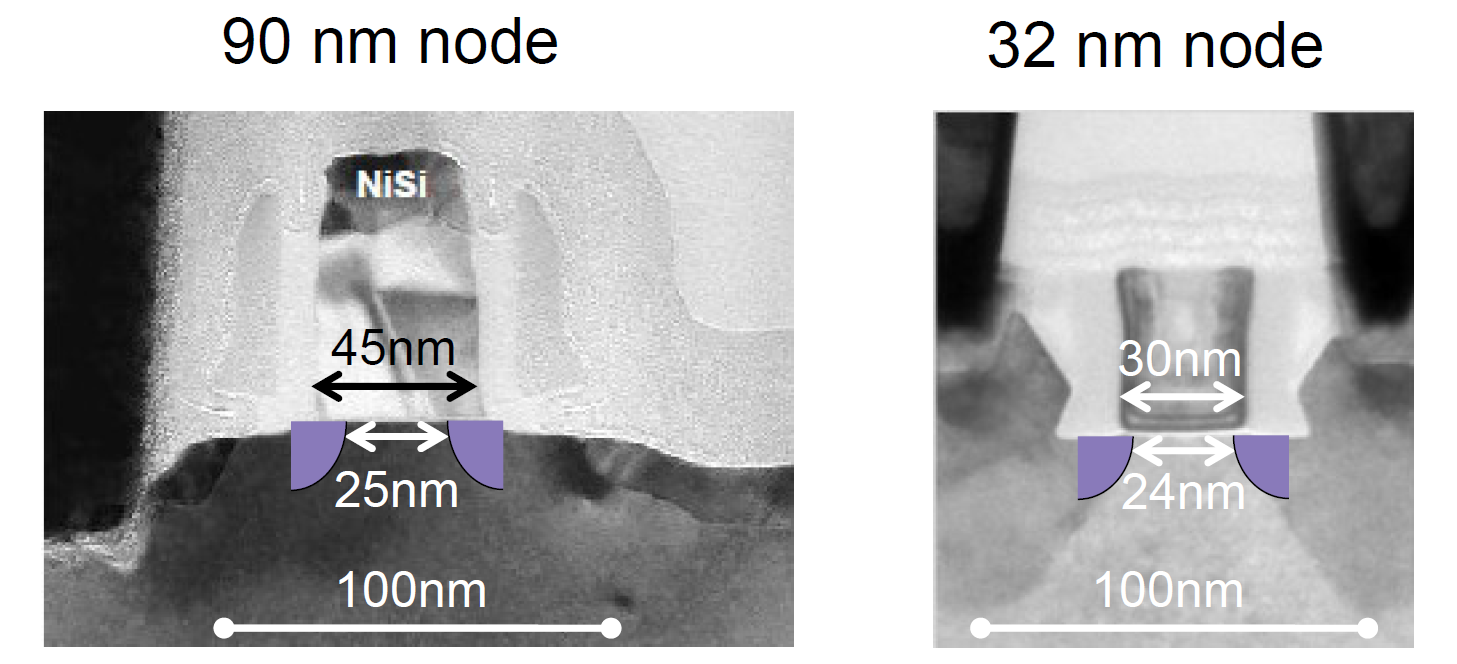
Micrograph of transistors made on 90 nm and 32 nm technical process. Zoom and scale are identical. A source
As we can see, the size of the metal contacts are smaller at times, but the width of the base has not changed much. All the same 25 nm. Moreover, for transistors using 14nm, 10nm and 7nm technology, it is the same ( ooops! ).
For the first time faced with this in the transition from 130 nm to the first series of 90 nm. Then for the first time they could not reduce the width of the base in proportion to all other sizes, it remained about 35 nm. Later, it was still reduced to 25 nm, but since then the width of the base has not been obeyed by the proportions of techno-forms. And the smaller the transistors became, the more this manifested.
It was necessary to change the criteria of norms of technical processes. What did you do? Most have done nothing. They continued to issue photolithographic resolution as a technical process rate. Or the minimum width of the plating track as a manifestation of the most simple and visual operation. And here we go to the maketing ...
The most creative are marketers from Intel. They began to calculate the rate of the technical process from the size of the elements, for example, on the basis of the area of the six-transistor cell of the static memory. In the technology with a resolution of 65 nm lithography, it was 0.77 μm 2 , and at a resolution of 40 nm it became 0.37 μm 2 . If the size of the transistors as previously decreased in proportion, then this corresponds to the technology of 45 nm. So we assume that we have 45 nm technology. Hence the discrepancies of tehnorm from Intel with others - 28 nm for all, 32 nm for Intel; 20 nm for all, 22 nm for Intel; 10 nm for all, 14 nm for Intel.
As the subsequent history showed, Intel in the end turned out to be more honest than its competitors.
Impact of leakage currents
There is a wonderful schedule from the article as much as 2010:
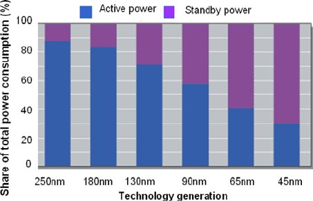
A source
The graph shows the percentage of working and parasitic energy consumption. Blue - energy release as a result of recharge currents (operating current), purple - the result of leakage currents (parasitic current). This is taking into account the measures that have been taken to reduce parasitic currents.
The reason why the clock speeds of the processors stopped has been clearly seen. The first processors at 3 GHz ( Pentium 4 , for example) appeared in the early 2000s. So at this level and remained. This is usually explained by the fact that the number of cores has increased, the logic has become more complicated, the pipelining has gone deeper, so the requirements for stability have increased and, in general, happiness is not in gigahertz. Partially true. But! Previously, they somehow managed to combine all these factors with increasing frequencies.
The fact is that earlier when reducing the size of transistors appeared reserve for power consumption. For example, the technology decreased by 2 times, the number of transistors increased 4 times, and the average power consumption of each transistor decreased by 6-7 times. The fact is that CMOS transistors consume current when switching, and the increase in the number of transistors was mainly due to the growth of cache memory. Memory transistors switch relatively rarely. Therefore, consumed less than the active elements of the processor.
This difference made it possible to raise the clock frequency at the same heat release.
In the transition from 180 nm to 130 nm, the leakage current ate this delta. Since then, in spite of all the tricks, the positive has not come out. All
In fact, over the course of the 2000s, there was a change of priorities in quiet glanders. Previously, the priority was to reduce the size of transistors, now - to reduce leaks.
About methods of dealing with leaks
Change of material of gate oxide
With the transition to High-k dielectrics and had to change the material of the gate. Instead of polysilicon, they began to reuse a metal, usually nickel silicide NiSi. For separation with the second and further layer of metallization, silicon oxide is still used.
Briefly about High-k dielectrics
One of the ways to improve the parameters of transistors was to reduce the thickness of the gate dielectric. There are many reasons. I will not go deep into physics, it is already overkill. In short, I will say that there is such a parameter as the gate capacitance. The system of shutter - dielectric - silicon resembles the flat capacitor model familiar from the course of school physics.
The main parameter of the capacitor - capacity. This is the ability of one plate to change the electrical state to the second without direct electrical contact. Unlike parasitic capacitances, the capacity of the shutter thing is useful. It characterizes the ability of the shutter to quickly induce a channel and collect as many charge carriers as possible in the near-surface layer. This minimizes the electrical resistance of the channel and the voltage drop. Capacity is determined by the formula:
S is the area of the plates,
d - the distance between them,
ԑ is the dielectric constant of the material between the plates, for vacuum 1, air is practically 1,
ԑ 0 is a dimensional constant.
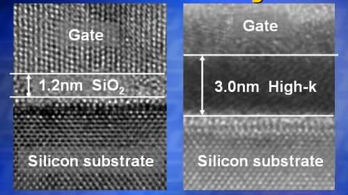
As the size reduced, the effective area of the shutter decreased. To compensate for it, the thickness of the gate oxide was reduced. As a result, they came to a thickness of 1.2 nm ( sic! ). These are 6 (!!!) atomic layers. At the same time received a decent tunnel leakage current from the gate to the silicon. The next step was to reduce the thickness to 5 atomic layers, i.e. up to 1 nm, with an increase in the tunneling current of 10 ( !!! ) times (with such dimensions, the probability of tunneling increases 10 times when approaching by 0.2 nm). Such leakage currents put an end to the stable operation of the microcircuit.
Therefore, the third component of the equation was used - the dielectric constant of the gate dielectric. We had to abandon the truly deserving silicon oxide in favor of materials with a higher dielectric constant - High-k dielectrics. This is usually hafnium oxide HfO 2 or tantalum oxide Ta 2 O 5 . The dielectric constant of silicon is 3.9, for High-k dielectrics 25-30. To provide the same capacity and the same distribution of strengths in the base, you can use a dielectric layer much thicker, because of which the tunneling currents from the gate are reduced by orders of magnitude.
The main parameter of the capacitor - capacity. This is the ability of one plate to change the electrical state to the second without direct electrical contact. Unlike parasitic capacitances, the capacity of the shutter thing is useful. It characterizes the ability of the shutter to quickly induce a channel and collect as many charge carriers as possible in the near-surface layer. This minimizes the electrical resistance of the channel and the voltage drop. Capacity is determined by the formula:
S is the area of the plates,
d - the distance between them,
ԑ is the dielectric constant of the material between the plates, for vacuum 1, air is practically 1,
ԑ 0 is a dimensional constant.
As the size reduced, the effective area of the shutter decreased. To compensate for it, the thickness of the gate oxide was reduced. As a result, they came to a thickness of 1.2 nm ( sic! ). These are 6 (!!!) atomic layers. At the same time received a decent tunnel leakage current from the gate to the silicon. The next step was to reduce the thickness to 5 atomic layers, i.e. up to 1 nm, with an increase in the tunneling current of 10 ( !!! ) times (with such dimensions, the probability of tunneling increases 10 times when approaching by 0.2 nm). Such leakage currents put an end to the stable operation of the microcircuit.
Therefore, the third component of the equation was used - the dielectric constant of the gate dielectric. We had to abandon the truly deserving silicon oxide in favor of materials with a higher dielectric constant - High-k dielectrics. This is usually hafnium oxide HfO 2 or tantalum oxide Ta 2 O 5 . The dielectric constant of silicon is 3.9, for High-k dielectrics 25-30. To provide the same capacity and the same distribution of strengths in the base, you can use a dielectric layer much thicker, because of which the tunneling currents from the gate are reduced by orders of magnitude.
Silicon on insulator (SOI)
Silicon technology on the insulator , also known as SOI, also known as SOI, was used before to isolate cells. Here they have gone even further: an oxide layer is formed on top of the silicon substrate, and a layer of silicon epitaxially builds up.
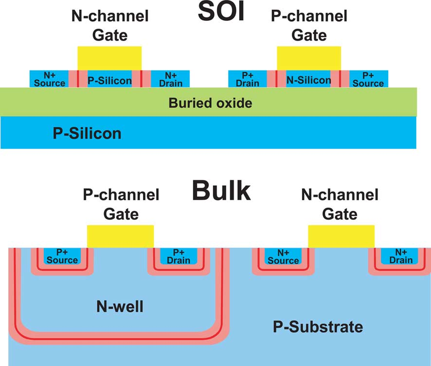
Schematically, the difference of SOI-technology with conventional planar MOS
This technology dramatically reduces leakage currents.
But there are drawbacks. SOI technology is still very complicated and expensive. In addition, due to the thin isolated base, there are problems with the accumulation of a sufficient number of electrons or holes to form a channel. The channel is very narrow. Another problem is the removal of heat. Silicon oxide has a low thermal conductivity, and the removal of heat from the film to the substrate mass is difficult.
Alternatively, instead of silicon oxide, you can use sapphire Al 2 O 3 , it has a higher thermal conductivity. Ideally, the oxide would have to be under the drain and the source, but it would not be under the base. Then, in combination with the High-k dielectric, it would be possible to increase the concentration of impurities in the base and reduce the channel width to 15 nm. However, the use of this technology is limited.
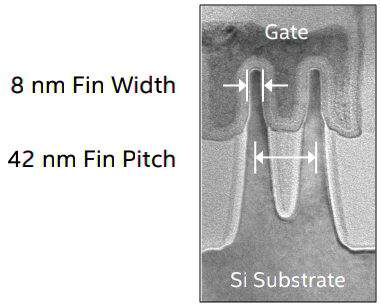
FinFET transistors
The name of the English Fin - fin, crest. The technology was first used on 22 nm technology and is currently dominant in the production of processors. The bottom line is that not a complete layer of silicon is epitaxially built up over the oxide, but individual ridges in the zones that are free from oxide.

For example, so. A source

Schematic comparison with planar technology - transistors become three-dimensional. A source
The shutter in this technology flows around the channel from three sides. When we apply voltage to the gate, it draws electrons (holes) from the depth to the tops of the crests, and a channel is formed in them. Thus, the entire active zone of the drain, source, and gate closes in the ridges, the leakage of currents deep into the substrate is minimal. In this case, thermally comb is not isolated from the substrate and the heat freely goes down.
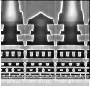
Usually use double or triple (triple) transistors. With such dimensions, it is impossible to make rectangular ridges as in the diagram; in shape, this is rather a truncated cone.
A source

The same
Bottom right is our CMOS transistor. We see 6 ridges, 3 for the n-channel, 3 for the p-channel (indicated as Fin in the figure), and in the middle across the gate (Gate), along the edges there are contacts to the drain and source. The size of the transistor is determined by the distance between the ridges, the number of ridges, the channel width (all the same 25 nm and more), the size of the drain and source areas. The resolution of photolithography affects the size of the transistor indirectly through the possibility of reducing the pitch between the ridges. For example, at 22 nm technology, the step between the crests of 54 nm, at 14 nm - 42 nm, at 10 nm - 34 nm. As we see here, linear dependence is not observed.
Now in the world there are only 3 companies that have mastered this technology. These are American Intel, Korean Samsung and Taiwanese TSMC. Even the former daughter of AMD - GlobalFoundries - dropped out of the process. Now AMD orders processors from TSMC and has entered into a contract with Samsung.
Little about metallization
Metal tracks in the first, bottommost layer of metallization have always been tried to be minimal. The fact is that the metallization path forms the same flat metal-insulator-silicon capacitor with silicon. But unlike the shutter, this is a parasitic capacitor. With a large capacity at frequencies in gigahertz, parasitic electrical connection may occur where it should not be. To reduce the parasitic capacitance you need to reduce the area of the tracks. Therefore, the tracks in the very first plating layer are made as short and as thin as possible. For the same reason, they try to have different layers of metallization overlap at a right angle — first, the longitudinal tracks are made, the next track is transverse tracks. The higher the layer, the thicker the oxide under it and the wider the track.
Why am I ?! Since the thickness of the first metal track is minimal, it is often indicated as the norm of the process. In FinFET technology, the space between ridges is filled with oxide. A rather thick layer on top of the High-k dielectric, gate, ridges and valleys. The first layer of metallization lead to these blockages above the depressions. The tracks themselves are made wider to reduce electrical resistance and compensate for irregularities. Those.the minimum possible width of the walkway and the reality also diverged.
Multi layer cake metallization
Those.the rate of technical process is increasingly becoming a virtual value. Therefore, we have processors with similar parameters, marked with norms from 7 nm to 22 nm. FinFET 22nm process allows you to get by with two crests, you need 3 crests in 7nm, as a result, the sizes of transistors are about the same. However, in journals it is often continued to write that with the transition from 10 nm to 7 nm the number of transistors will increase 1.8 times. People still have the old templates of the era of Moore ...
What next?The transition to bulk transistors led to the emergence of a large number of promising modifications. For example, Samsung announced GAAFET technology for technology at 5 nm.

Comparison of CMOS, FinFET and GAAFET clearly. A source
Those.the comb should not be solid, but divided into separate threads. The question is: is it worth it? - remains open.
There are also options for ring closures, vertical, etc. There are combinations of FinFET and SOI. In general, chemical epitaxy processes are more complex, but more linear and predictable than lithography. It provides used for greater accuracy and the ability to create more subtle three-dimensional structure.
Situation in the modern market of microprocessor manufacturers and prospects
So, the top three stand out - Intel, Samsung and TSMC. Intel conducts under its own brands, the rest mainly to order. Under the brands of AMD, NVIDIA, Qualcomm, Apple, IBM hiding chips manufactured in factories TSMC or Samsung. Some old leaders fell off or rested against a barrier. The Chinese are trying to break through to the big leagues, but not very successfully so far: they lack their own technological base, and world leaders in the production of equipment keep the latest technological lines for the Chinese.
The experts' optimism is associated with the transition to three-dimensional structures and the beginning of the use of EUV-lithography. Samsung and TSMC began to use it for the most delicate structures. This gives them the opportunity to report on the achievement of standards at 7 nm and in the future up to 5 nm. Although, as already described, these figures actually have little effect. The same Intel refused from EUV at all. Apparently, they do not believe that this will greatly improve the performance.
On the other hand, people in the subject understand that the era of Moore is over, and each new step of productivity growth will require all the greater effort and time. The rapid growth of microelectronics ends ( sob! ). As it happened once in the automotive and aircraft industry. After explosive growth, slow development follows.
From promising breakthrough points, we can distinguish the transition to another material (not silicon) and the creation of multilayer chips (3D integration - hi AMD ideas). For 3D integration, you will have to drastically reduce heat generation or increase heat dissipation.
That's all about the size of the transistors. B of lshie reserves of productivity growth has in the other. In an optimization architecture, for example. You can even make a marketing move, saying that a new processor with an improved architecture works as if it were old with 0.5 nm technology. Therefore, we mark it as 0.5 nm. And figs with him that the dimensions of the transistors are the same.
It is possible to create new types of cells from combinations of transistors. For example, instead of 6 transistor memory cells, make 2 transistor structures with complex interaction physics. Bulk structures here provide many possibilities.
Limiting physical limitations
Someone may say that the pessimism of the author is not justified. Find ways to circumvent the restrictions. Maybe not as fast as before, but nonetheless.
The fact is that there are still physical processes that cannot be circumvented. The main of them - the substance consists of atoms, and charge carriers are electrons. Create a transistor smaller than an atom does not work. It can not create even less than 1000 atoms. Because there is an electron and the Heisenberg uncertainty relation. An electron is a very unstable particle, more or less stable behavior is possible only for an array of thousands and millions of electrons. On one electron, you can only kill the cat Schrödinger.
Note: although there are developments on single-electron transistors ( 1 , 2 and3 )
Even with the current size collisions occur, due to the spontaneous operation of transistors. If the probability of a collision is 10 -9 (one per billion), then with the number of elements in billions and frequencies in GHz, this gives an average of 1 collision per cycle, or several billion collisions per second. To catch these, there are systems for monitoring the integrity of operations, and a suspicious operation is sent to be re-executed.
As miniaturization proceeds, the number of collisions begins to grow very sharply. As a result, we arrive at a situation of zero or even negative effect from miniaturization. Those.the transistors did less, they fit into the crystal more, but due to the growth of collisions and re-processing cycles, the total performance has not increased. Or maybe even fell. And this threshold is quite on the horizon.
A few words about domestic digital microelectronics
Contrary to popular belief, until 1985, the backlog of the USSR from the leaders was not so great. About 3-4 years. This is if we take the enterprise-leaders in Zelenograd (note: about Micron BarsMonster wrote at the time ). In the conditions of Moore’s law, even a lag of 3-4 years strongly influenced the characteristics. There were problems with obtaining high-quality oxide, with the clarity of pn-junctions. If we add to this a conservative policy of packing chips into the case (long contact lines did not contribute to an increase in device performance), as well as the Soviet standards for the production of boards and cases with a lot of iron (who disassembled Soviet tape recorders, he will understand), we get an anecdote about the Soviet iron-chip circuit carrying handles.
The reasons for the lag are many. Later startanuli, limited resources, dispersion of resources. When Americans focused on CMOS, we continued to experiment with various technologies. Quite actively worked with alternatives to silicon, primarily with materials A 3 B 5 . Well, the general relaxation of the late Soviet research institutes.
After 1985, the Americans started off abruptly, and we started having problems. Further, the 1990s, when life in the industry was warming by inertia. As a result, in the 21st century came with the technology of 800 nm, when the leaders had already stormed 130 nm. The second life of the industry was given by mass cardization and government orders. The main production of steel: chips for SIM-cards, bank cards, payment cards, transport and discount cards and other consumer goods. There do not need large gigahertz and small nanometers.
Note: by the way, while one-time tickets operate in Msk (bought-used-threw-loaded the plant), in the same China they actively promote resource-saving technologies, in particular, reusable use of the "token" on the subway (even for one short trip) .
Video about subway Shenzhen
Nevertheless, there is an attempt to get into the "major league" of microelectronics. The development goes in four main directions.
- "Sovereign" tehprotsessy. An attempt to create a complete production cycle on the equipment of domestic production and own technical processes. We are going the same way that leaders have gone about 20 years ago, but taking into account the found rakes and solutions. From the last that was in open sources it is 250 nm in series and 150 nm in the process of implementation. Here we can also include an attempt to create our own installations of EUV-lithography at 13.5 nm and thus immediately go out, if not in the big league, then close to them.
- . , . , . . «» AMD 2007, 180 . «» 90 STMicroelectronics 65 . , . – .
- . ,
. . , . -, . – .
.: 28 TSMC. . - . , . A 3 B 5 , . - , .
.: , OptoGaN , .
In general, for the Russian microelectronics situation is not brilliant. But there is a hope that the leaders will inevitably slow down due to physical constraints, and here we are slowly hurrying up, sneaking up behind us.
The final chord about memory and windows of opportunity in the third part in a couple of days - stay tuned!
Do not forget to subscribe to the blog : You are not difficult - I am pleased!
And yes, about the defects noted in the text, please write in the LAN.
Source: https://habr.com/ru/post/456298/
All Articles