Legendary Intel Core i7-2600K: Sandy Bridge Testing in 2019 (Part 1)
Part 1 >> Part 2 >> Part 3
One of the most popular processors of the past decade was the Intel Core i7-2600K. The design was revolutionary, as it offered a significant leap in performance and efficiency of the single-core processor, and the processor itself was also well-able to overclock. The next several generations of Intel processors did not look so interesting, and often did not give users a reason for the upgrade, so the phrase "I will stay with my 2600K" became ubiquitous on forums and sounds even today. In this review, we shook dust from the box with the old processors and drove the veteran through a set of benchmarks in 2019, both at the factory settings and in overclocking, to make sure that he is still the champion.
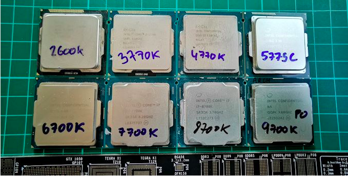
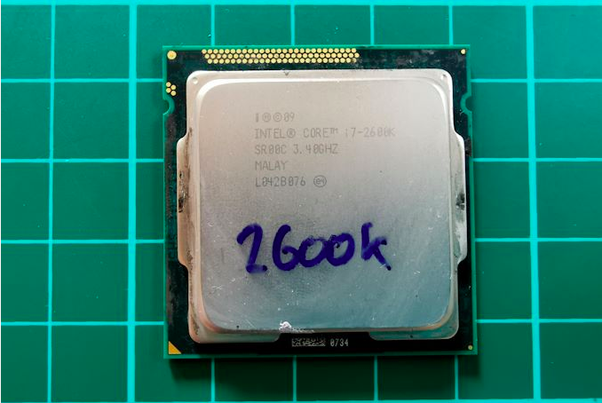
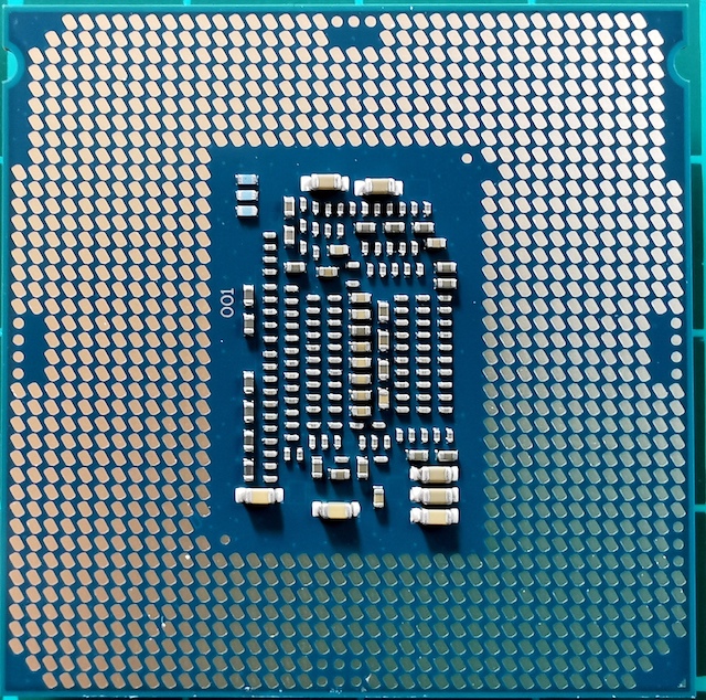
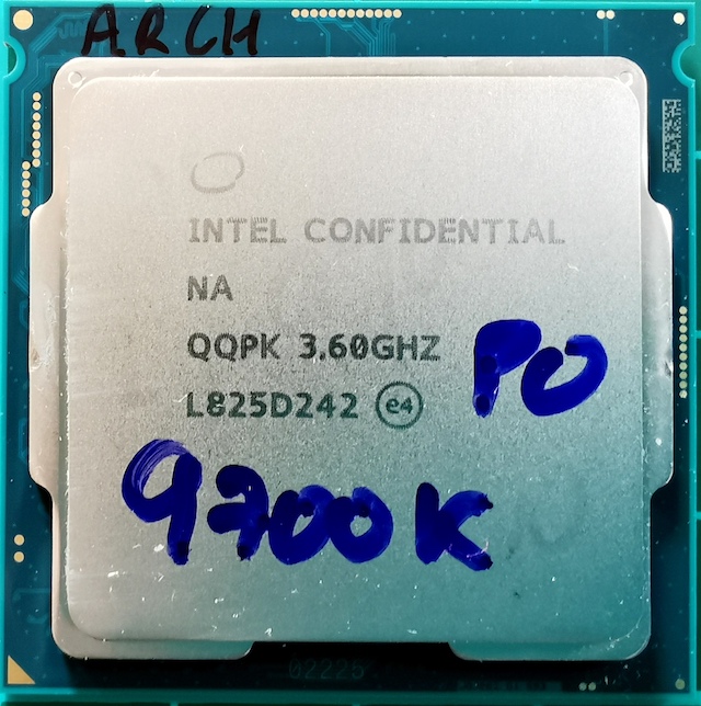
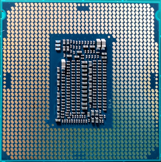
“Family photo” Core i7
')
Sit in a chair, sit back and imagine yourself in 2010. It was the year when you looked at your outdated Core 2 Duo or Athlon II system, and realized that the time had come for an upgrade. You are already familiar with the architecture of Nehalem, and you know that the Core i7-920 accelerates well and makes competitors. It was a good time, but suddenly Intel changed the balance in the industry, and created a truly revolutionary product. Echoes of nostalgia for which are heard so far.
Core i7-2600K: the fastest Sandy Bridge (up to 2700K)
This new product was Sandy Bridge. AnandTech released an exclusive review, and the results were almost impossible to believe, for many reasons. According to our tests of that time, the processor was simply incomparably higher than anything we saw before, especially considering the Pentium 4 thermal monsters that were released several years before. The core upgrade, based on Intel's 32nm process technology, has become the biggest turning point in x86 performance, and since then we have not seen such breakthroughs. AMD will need another 8 years to get its moment of glory with the Ryzen series. Intel also managed to take advantage of the success of its best product, and get a place champion.
In this basic design, Intel did not skimp on innovation. One of the key elements was the micro-op cache. This meant that the newly decoded instructions, which were required again, were taken already decoded, instead of wasting energy on re-decoding. At Intel with Sandy Bridge, and much later at AMD with Ryzen, the inclusion of a micro-operation cache became a miracle for single-threaded performance. Intel also began to improve simultaneous multithreading (which for several generations was called HyperThreading), gradually working to dynamically distribute the computing streams.
The quad-core design of the best processor at the time of launch, the Core i7-2600K, became the backbone of the products in the next five generations of Intel architecture, including Ivy Bridge, Haswell, Broadwell, Skylake and Kaby Lake. Since the days of Sandy Bridge, although Intel has moved to a smaller technological process, and has taken advantage of lower power consumption, the corporation has not been able to recreate this exceptional leap in the net bandwidth of the teams. Later, the growth for the year was 1-7%, mainly due to an increase in operating buffers, ports of execution and support for commands.
Since Intel was unable to repeat the Sandy Bridge breakthrough, and the core microarchitecture was the key to x86 performance, users who purchased the Core i7-2600K (I bought two) remained on it for a long time. Largely due to the expectation of another big performance leap. And over the years, their disappointment is growing: why invest in a quad-core Kaby Lake Core i7-7700K with a clock frequency of 4.7 GHz, while your quad-core Sandy Bridge Core i7-2600K is still overclocked to 5.0 GHz?
(Intel’s responses usually relate to power consumption and new features such as how the GPU and drives work through PCIe 3.0. But some users were not satisfied with these explanations.)
That is why the Core i7-2600K has identified a generation. It remained in force, at first to the joy of Intel, and then to the disappointment when users did not want to be updated. Now, in 2019, we understand that Intel has already gone beyond the four cores in its main processors, and, if the user is worth the price of DDR4, he can either switch to the new Intel system or choose the AMD path. But the question is how the Core i7-2600K copes with workloads and games in 2019; or, more precisely, how does the overclocked Core i7-2600K cope?
In truth, the Core i7-2600K was not the fastest mainstream Sandy Bridge processor. A few months later, Intel launched a slightly more “high-frequency” 2700K on the market. It worked almost the same, and accelerated in a similar way to 2600K, but it cost a little more. By this time, users who saw a jump in performance and made an upgrade were already at 2600K, and stayed with it.
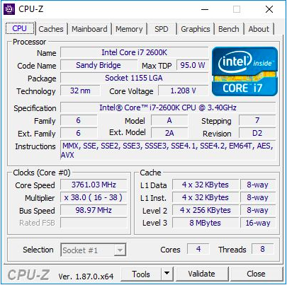
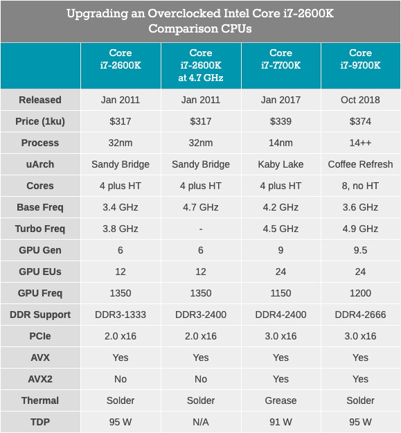
Core i7-2600K was a 32-nm quad-core processor with HyperThreading technology, with a base frequency of 3.4 GHz, a turbo frequency of 3.8 GHz, and with a nominal TDP of 95 watts. At that time, Intel's TDP was not yet divorced from reality: in our testing for this article, we saw a peak power consumption of 88 watts on an unclocked CPU. The processor came with integrated graphics Intel HD 3000 and supports DDR3-1333 memory by default. Intel has set the price of 317 dollars at the start of the chip.
For this article, I used the second i7-2600K, which I bought when they first appeared. It was tested both at the nominal frequency and overclocked to 4.7 GHz on all cores. This is average overclocking - the best of these chips operate at 5.0 GHz - 5.1 GHz in everyday mode. In fact, I remember well how my first Core i7-2600K worked at 5.1 GHz on all cores, and even 5.3 GHz (also on all cores), when during an overclocking competition in the middle of winter, at room temperature At a temperature of around 2C, I used a powerful liquid cooler and 720mm radiators. Unfortunately, over time, I damaged this chip, and now it does not load even at the nominal frequency and voltage. Thus, we have to use my second chip, which was not so good, but still able to give an idea of the operation of the overclocked processor. In overclocking, we also used overclocked memory, DDR3-2400 C11.
It is worth noting that since the launch of the Core i7-2600K, we switched from Windows 7 to Windows 10. The Core i7-2600K does not support AVX2 instructions, and was not created for Windows 10, so it will be particularly interesting to see how this appears on the results.

Core i7-7700K: The latest quad-core Intel Core i7 with HyperThreading technology
The fastest and newest (and latest?) Quad-core processor with HyperThreading, released by Intel, was the Core i7-7700K, a representative of the Kaby Lake family. This processor is based on Intel's improved 14-nm process technology, operates at a base frequency of 4.2 GHz and a turbo frequency of 4.5 GHz. Its TDP with a rated power of 91 W in our testing showed a power consumption of 95 watts. It comes with Intel Gen9 HD 630 graphics and supports standard DDR4-2400 memory. Intel has released a chip with a declared price of 339 dollars.
Along with the 7700K, Intel also released its first overclocked dual-core processor with hyper-trading - Core i3-7350K. In the course of this review, we overclocked such a Core i3 and compared it with the Core i7-2600K on the factory settings, trying to answer the question of whether Intel was able to achieve a dual-core processor performance similar to their old quad-core flagship. As a result, while i3 prevailed in single-threaded performance and memory management, the lack of a pair of cores made most of the tasks too hard for Core i3.
Core i7-9700K: The Latest Intel Core i7 Top (Now With 8 Cores)
Our latest processor for testing is the Core i7-9700K. In the current generation, this is no longer the flagship of Coffee Lake (now it's i9-9900K), but it has eight cores without hyper-trading. The comparison with the 9900K, which has twice the number of cores and threads, looks meaningless, especially when the price of i9 is 488 dollars. In contrast, the Core i7-9700K is sold in bulk “only” at $ 374, with a base frequency of 3.6 GHz and a turbo frequency of 4.9 GHz. Its TDP is determined by Intel at 95 W, but on the consumer motherboard the chip consumes ~ 125 W at full load. DDR4-2666 memory is supported as standard.
Core i7-2600K has to work with DDR3, supports PCIe 2.0, not PCIe 3.0, and is not designed to work with NVMe drives (which are not involved in this testing). It will be interesting to see how close the overclocked veteran is to the Core i7-7700K, and what growth we will see when moving on to something like the Core i7-9700K.
In 2019, we are talking about chips 100-200 mm2 in size, with up to eight high-performance cores, and created on the latest versions of the Intel or AMD GlobalFoundries / TSMC process technology. But 32nm Sandy Bridge was a completely different beast. The production process was still “flat”, with no FinFET transistors. In the new CPU, the second generation High-K was implemented, and the scale of 0.7x was achieved compared to the previous, larger 45-nm process technology. The Core i7-2600K was the largest quad-core chip, and contained 1.16 billion transistors per 216 mm2. For comparison, the newest Coffee Lake processor at 14 nm accommodates eight cores and more than 2 billion transistors in an area of ~ 170 mm2.
The secret to a huge jump in performance lies in the microarchitecture of the processor. Sandy Bridge promised (and provided) significant performance at equal clock speeds, compared with previous-generation Westmere processors, and also formed the basic circuit for Intel chips for the next decade. Many of the key innovations first appeared in retail sales with the advent of Sandy Bridge, and then many iterations were repeated and improved, gradually reaching the high productivity that we use today.
In this review, I relied heavily on Anandtech’s initial 2600K micro-architecture report, which was released in 2010. Of course, with some additions based on a modern look at this processor.
For those new to the development of processors, here’s a quick overview of how an extraordinary processor works. In short, the kernel is divided into external and internal interfaces (front end and back end), and the data is first fed to the external interface.
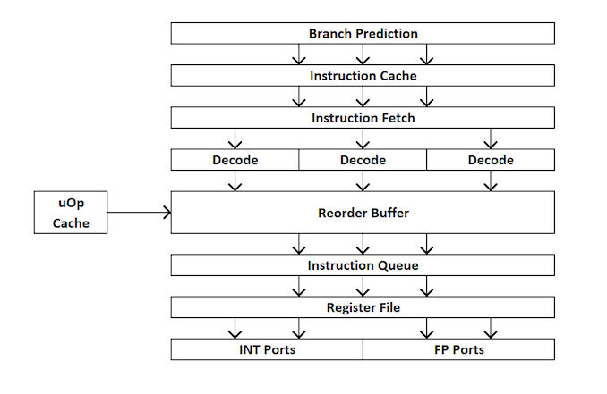
In the external interface, we have the means of prefetching and branch predictors, which will predict and extract instructions from the main memory. The idea is that if you can predict what data and instructions will be needed in the near future (before they are in demand), then you can save time by placing this data close to the core. The instructions are then placed into a decoder, which converts the bytecode instruction into a series of “micro-operations”, which the kernel can then process.
There are different types of decoders for simple and complex instructions - simple x86 instructions are easily mapped to one micro-operation, while more complex instructions can be decoded into more operations. The ideal situation is the lowest possible decoding rate, although sometimes instructions can be divided into more micro-operations if these operations can be performed in parallel (command-level parallelism or ILP).
If the kernel has a micro-operation cache, also known as the uOp cache, then the results of each decoded instruction are stored in it. Before the instruction is decoded, the kernel checks whether this particular command has been decoded recently, and if successful, uses the result from the cache instead of re-decoding, which consumes energy.
Now micro-operations are being put on “placement queues” - the allocation queue. A modern core can determine whether instructions are part of a simple loop, or uOps (micro-operations) can be combined to speed up the whole process. Then, uOps are fed into the re-order buffer, which forms the “back end” of the kernel.
In the backend, starting with the re-order buffer, uOps can be rearranged depending on where the data needed by each micro-operation is located. This buffer can rename and distribute micro-operations, depending on where they should go (integer operations or FP), and, depending on the kernel, it can also act as a mechanism for deleting completed instructions. After re-ordering, the uOps buffer is sent to the scheduler in the right order to make sure the data is ready, and to maximize the throughput of the uOp.
The scheduler transmits uOps to the execution ports (to perform calculations) as needed. Some cores have a single scheduler for all ports, but in some cases it is divided into a scheduler for integer / vector operations. Most kernels with an extraordinary execution have from 4 to 10 ports (some more), and these ports perform the necessary calculations in order for the instruction to “pass” through the kernel. Execution ports can take the form of a load module (load from the cache), a storage module (save in cache), a module of integer mathematical operations, a module of mathematical operations with a floating point, as well as vector mathematical operations, special division modules, and some others for special operations . After the execution port has been processed, data can be stored in the cache for reuse, placed in the main memory; at this time, the instruction is sent to the delete queue, and finally deleted.
This brief overview does not address some of the mechanisms that modern kernels use to facilitate caching and searching for data, such as transaction buffers, stream buffers, tagging, etc. Some mechanisms are iteratively improved with each generation, but usually when we talk about “instructions” per clock ”as an indicator of performance, we strive to“ skip ”as many instructions as possible through the core (through the frontend and backend). This figure depends on the decoding speed at the processor frontend, command prefetching, re-order buffer, and maximum use of execution ports, along with the removal of the maximum number of commands executed per clock cycle.
In view of the above, we hope that the reader will be able to more fully understand the Anandtech test results obtained during the launch of Sandy Bridge.
The CPU architecture of Sandy Bridge looks evolutionary with a brief overview, but it is revolutionary in terms of the number of transistors that have changed since the days of Nehalem / Westmere. The most important change for Sandy Bridge (and all microarchitectures after it) is the micro-operation cache (uOp cache).

A micro-operation cache appeared in Sandy Bridge, which caches instructions after they are decoded. There is no complicated algorithm, decoded instructions are simply saved. When the Sandy Bridge prefetcher receives a new instruction, it first searches for the instruction in the micro-operations cache, and if it is found, the rest of the pipeline will work with the cache, and the front end will be disabled. Decoding hardware is a very complex part of the x86 pipeline, and turning it off saves a significant amount of energy.
This is a direct mapping cache, and can store approximately 1.5 KB of micro-ops, which is actually equivalent to the 6 KB of instructions cache. The micro-op cache is included in the L1 instruction cache, and its Hit Rate for most applications reaches 80%. The micro-operation cache has a slightly higher and stable throughput compared to the instruction cache. The actual L1 command and data caches have not changed, they still constitute 32 KB each (64 KB L1 in total).
All instructions coming from the decoder can be cached by this mechanism, and, as I said, there are some special algorithms in it - simply, all instructions are cached. Long-unused data is deleted when space ends. A microoperational cache may seem similar to the tracing cache in Pentium 4, but with one significant difference: it does not cache traces. This is simply an instruction cache in which micro-operations are stored instead of macro-operations (x86 instructions).
Along with the new micro-cache, Intel also introduced a completely redesigned branch prediction module. The new BPU is about the same as its predecessor, but much more accurate. The increase in accuracy is the result of three major innovations.
The standard branch predictor is a 2-bit predictor. Each branch is marked in the table as accepted / not accepted with appropriate reliability (strong / weak). Intel found that almost all the branches predicted by this bimodal predictor have “high” confidence. Therefore, in Sandy Bridge, a bimodal branch predictor uses one confidence bit for multiple branches, rather than one confidence bit for each branch. As a result, your branch history table will be the same as before, the number of bits that represent many more branches, which leads to more accurate predictions in the future.
With the growth of multi-core processors, managing the flow of data between cores and memory has become an important topic. We have seen many different ways to move data around the CPU, such as crossbar (cross), ring (ring), mesh (mesh), and, later, completely separate I / O chips. The battle of the next decade (2020+), as mentioned earlier by AnandTech, will be a battle of inter-core connections, and now it is already beginning.
The feature of Sandy Bridge is that it was Intel's first consumer CPU, which used a ring bus connecting all the cores, memory, last-level cache, and integrated graphics. This is still the same design that we see in modern Coffee Lake processors.
In Nehalem / Westmery Bridge adds a graphics processor and video transcoding engine to the chip, which share the L3 cache. And instead of running more wires to the L3, Intel introduced the ring bus.
Architecturally, this is the same ring bus used in the Nehalem EX and Westmere EX. Each core, each fragment of the L3 cache (LLC), the integrated graphics processor, the media engine, and the system agent (a funny name for the north bridge) are attached to the ring bus. A bus consists of four independent rings: a data bus, requests, acknowledgments, and a state monitoring bus. Each call to any of the rings can transmit 32 bytes of data per clock. As the number of cores and the size of the cache increases, the throughput of your cache increases accordingly.
Each core in the end accounts for the same amount of L3 cache bandwidth as in high-performance Westmere processors — 96 GB / s. Sandy Bridge’s aggregate throughput is 4 times higher than the Westmere quad-core because it simply multiplies by the number of cores and is 384 GB / s.
This means that the L3 latency is significantly reduced from about 36 clocks in Westmere to 26 to 31 clocks in Sandy Bridge (with some variable cache delay, which depends on which core accesses which fragment of cache). In addition, unlike Westmere, the L3 cache now runs at the core clock — the un-Core concept still exists, but Intel calls the extra-core part the “system agent” and no longer includes the L3 cache. (The term "un-Core" is still used today to describe interconnects.)
Thanks to the L3 cache, which runs at the core frequency, you get the benefits of a much faster cache. The disadvantage is that L3 accelerates with the processor cores when turbo or idle modes are enabled. If the graphics processor needs L3, when the core frequency is lowered, the L3 cache will not work as fast as if it were independent. Or the system will have to overclock the core and consume additional power.
L3 cache is divided into fragments, each of which is associated with a separate core. Because Sandy Bridge has a fully accessible L3 cache, each core can address the entire cache. Each fragment has its own bus access controller, and a full cache pipeline. In Westmere, there was one cache pipeline and a queue to which all the kernels sent requests, but in Sandy Bridge they are distributed into cache segments. Using a ring bus means adding new access points to the bus has ceased to critically affect the size of the matrix. Despite the fact that each user of the ring receives its own controller, the data always follow the shortest path. Bus control is distributed throughout the ring, and as a result, each module “knows” whether the empty slot on the bus was one clock back.
For some reason, Intel stopped using the un-core term in SB, and Sandy Bridge called this part “system agent”. (Again, un-core is now back in fashion for interconnects, I / O, and memory controllers). The system agent is a traditional North Bridge. You have 16 PCIe 2.0 lanes available, which can be divided into two x8 channels. There is a reworked dual-channel DDR3 memory controller, which finally provides memory latency at about Lynnfield (Clarkdale moved the memory controller from the CPU to the graphics processor).
The system agent also has a DMI interface, a video output unit and a PCU (power management unit). The clock frequency of SA is lower than that of the rest of the core, and has a separate power scheme.
Another major performance improvement Sandy Bridge has in comparison to Westmere is graphics processing. While the processor cores show a performance improvement of 10-30%, Sandy Bridge's graphics performance is simply twice as high as that of Intel products before Westmere (Clarkdale / Arrandale). Despite the jump from 45 nm to 32 nm, the graphics processing speed improves due to a significant increase in IPC.
The Sandy Bridge GPU is built on the same 32nm transistors as the processor cores. The graphics processor is in its own little world in terms of power and frequency. The GPU can be turned off or on regardless of the processor. Graphic turbo is available for both desktop and mobile processors.
The GPU is treated as an equal citizen in the Sandy Bridge world, and gets full access to the L3 cache. The graphics driver controls what exactly gets into the L3 cache, and you can even limit the amount of cache that is available to the graphics processor. Storing graphics in the cache is especially important because it reduces recourse to main memory, which are costly both in terms of performance and in terms of power consumption. But rebuilding the graphics processor to use the cache is not an easy task.
SNB graphics (internal name Gen 6) make extensive use of hardware with fixed functions. The idea is this: everything that can be described using a fixed function, which must be implemented by a hardware fixed function. The advantage is performance, power and reduced matrix size, albeit at the cost of loss of flexibility.
Programmable shader hardware consists of shaders / cores / execution units, which Intel calls the EU. Each EU can accept instructions from multiple threads. Internal ISA is mapped one-to-one to most DirectX 10 API instructions, meaning a CISC-like architecture. The transition from a one-to-one API to display instructions increases IPC by effectively increasing the width of the EU.
There are other improvements in the EU. Transcendental mathematics is processed by hardware in the EU, and its performance has increased significantly. Intel then reported that sine and cosine operations are now several orders of magnitude faster than in graphics to Westmere.
Intel's previous graphics architectures have been redistributed on the fly. If a stream requires fewer registers, the remaining registers can be allocated to another stream. Despite the fact that it was an excellent approach to save the area of the matrix, it turned out to be a performance limiter. Often the threads could not be processed because there were no registers available for use. Intel increased the number of registers per stream first from 64 to 80, and then to 120 for Sandy Bridge. Downtime scenarios due to a lack of registers have been significantly reduced.

In sum, all these improvements have doubled the throughput of instructions in the EU.
At launch, there were two versions of the Sandy Bridge GPU: one with 6 EU and one with 12 EU. All mobile processors (at startup) use 12 EU, while in desktop SKUs 6 or 12 can be used, depending on the model. Sandy Bridge was a step in the right direction for Intel, as integrated graphics began to become mandatory for consumer products, and Intel gradually began to increase the percentage of chip space allocated to the GPU. Modern (2019) desktop processors of a similar level have 24 EU (Gen 9.5), while future 10-nm processors will have ~ 64 EU (Gen11).
Next to the Sandy Bridge GPU is a media processor. SNB media processing consists of two main components: video decoding and video encoding.
The hardware accelerated decoding mechanism has been improved compared to the current generation: now the entire video pipeline has been decoded using modules with fixed functions. This contrasts with Intel's pre-SNB design, which uses an EU array for some video decoding stages. As a result, Intel claims that the power consumption of the SNB processor is halved when playing HD video.
The video encoding engine was a completely new addition to Sandy Bridge. Intel took a ~ 3-minute original 1080p 30 Mbit / s video and recoded it into an iPhone 640 x 360 video format. The whole process took 14 seconds and ended at about 400 frames per second.
The principle of encoding / decoding by a fixed function is now common in any graphics hardware for desktops and even smartphones. At that time, Sandy Bridge used 3 mm2 matrices for this basic encoding / decoding structure.
Lynnfield Intel, . , TDP 95 , , , -.
, - . , , — , .
Sandy Bridge , PCU TDP ( 25 ). PCU , . , , TDP. , , TDP, , , TDP. SNB TDP, PCU .

Both CPU and GPU Turbo can work in tandem. Workloads that are more related to GPUs running on SNBs can lead to lower CPU core frequencies and higher GPU frequencies. Also, tasks related to the CPU can reduce the frequency of the GPU and increase the frequency of the CPU. Sandy Bridge as a whole turned out to be a much more flexible mechanism than anything that was created before it.
Thank you for staying with us. Do you like our articles? Want to see more interesting materials? Support us by placing an order or recommending to friends, 30% discount for Habr's users on a unique analogue of the entry-level servers that we invented for you: The Truth About VPS (KVM) E5-2650 v4 (6 Cores) 10GB DDR4 240GB SSD 1Gbps $ 20 or how to share the server? (Options are available with RAID1 and RAID10, up to 24 cores and up to 40GB DDR4).
Dell R730xd 2 times cheaper? Only we have 2 x Intel TetraDeca-Core Xeon 2x E5-2697v3 2.6GHz 14C 64GB DDR4 4x960GB SSD 1Gbps 100 TV from $ 199 in the Netherlands! Dell R420 - 2x E5-2430 2.2Ghz 6C 128GB DDR3 2x960GB SSD 1Gbps 100TB - from $ 99! Read about How to build an infrastructure building. class c using servers Dell R730xd E5-2650 v4 worth 9000 euros for a penny?
One of the most popular processors of the past decade was the Intel Core i7-2600K. The design was revolutionary, as it offered a significant leap in performance and efficiency of the single-core processor, and the processor itself was also well-able to overclock. The next several generations of Intel processors did not look so interesting, and often did not give users a reason for the upgrade, so the phrase "I will stay with my 2600K" became ubiquitous on forums and sounds even today. In this review, we shook dust from the box with the old processors and drove the veteran through a set of benchmarks in 2019, both at the factory settings and in overclocking, to make sure that he is still the champion.
“Family photo” Core i7
')
Why the 2600K was decisive for the generation
Sit in a chair, sit back and imagine yourself in 2010. It was the year when you looked at your outdated Core 2 Duo or Athlon II system, and realized that the time had come for an upgrade. You are already familiar with the architecture of Nehalem, and you know that the Core i7-920 accelerates well and makes competitors. It was a good time, but suddenly Intel changed the balance in the industry, and created a truly revolutionary product. Echoes of nostalgia for which are heard so far.
Core i7-2600K: the fastest Sandy Bridge (up to 2700K)
This new product was Sandy Bridge. AnandTech released an exclusive review, and the results were almost impossible to believe, for many reasons. According to our tests of that time, the processor was simply incomparably higher than anything we saw before, especially considering the Pentium 4 thermal monsters that were released several years before. The core upgrade, based on Intel's 32nm process technology, has become the biggest turning point in x86 performance, and since then we have not seen such breakthroughs. AMD will need another 8 years to get its moment of glory with the Ryzen series. Intel also managed to take advantage of the success of its best product, and get a place champion.
In this basic design, Intel did not skimp on innovation. One of the key elements was the micro-op cache. This meant that the newly decoded instructions, which were required again, were taken already decoded, instead of wasting energy on re-decoding. At Intel with Sandy Bridge, and much later at AMD with Ryzen, the inclusion of a micro-operation cache became a miracle for single-threaded performance. Intel also began to improve simultaneous multithreading (which for several generations was called HyperThreading), gradually working to dynamically distribute the computing streams.
The quad-core design of the best processor at the time of launch, the Core i7-2600K, became the backbone of the products in the next five generations of Intel architecture, including Ivy Bridge, Haswell, Broadwell, Skylake and Kaby Lake. Since the days of Sandy Bridge, although Intel has moved to a smaller technological process, and has taken advantage of lower power consumption, the corporation has not been able to recreate this exceptional leap in the net bandwidth of the teams. Later, the growth for the year was 1-7%, mainly due to an increase in operating buffers, ports of execution and support for commands.
Since Intel was unable to repeat the Sandy Bridge breakthrough, and the core microarchitecture was the key to x86 performance, users who purchased the Core i7-2600K (I bought two) remained on it for a long time. Largely due to the expectation of another big performance leap. And over the years, their disappointment is growing: why invest in a quad-core Kaby Lake Core i7-7700K with a clock frequency of 4.7 GHz, while your quad-core Sandy Bridge Core i7-2600K is still overclocked to 5.0 GHz?
(Intel’s responses usually relate to power consumption and new features such as how the GPU and drives work through PCIe 3.0. But some users were not satisfied with these explanations.)
That is why the Core i7-2600K has identified a generation. It remained in force, at first to the joy of Intel, and then to the disappointment when users did not want to be updated. Now, in 2019, we understand that Intel has already gone beyond the four cores in its main processors, and, if the user is worth the price of DDR4, he can either switch to the new Intel system or choose the AMD path. But the question is how the Core i7-2600K copes with workloads and games in 2019; or, more precisely, how does the overclocked Core i7-2600K cope?
Find the Differences: Sandy Bridge, Kaby Lake, Coffee Lake
In truth, the Core i7-2600K was not the fastest mainstream Sandy Bridge processor. A few months later, Intel launched a slightly more “high-frequency” 2700K on the market. It worked almost the same, and accelerated in a similar way to 2600K, but it cost a little more. By this time, users who saw a jump in performance and made an upgrade were already at 2600K, and stayed with it.
Core i7-2600K was a 32-nm quad-core processor with HyperThreading technology, with a base frequency of 3.4 GHz, a turbo frequency of 3.8 GHz, and with a nominal TDP of 95 watts. At that time, Intel's TDP was not yet divorced from reality: in our testing for this article, we saw a peak power consumption of 88 watts on an unclocked CPU. The processor came with integrated graphics Intel HD 3000 and supports DDR3-1333 memory by default. Intel has set the price of 317 dollars at the start of the chip.
For this article, I used the second i7-2600K, which I bought when they first appeared. It was tested both at the nominal frequency and overclocked to 4.7 GHz on all cores. This is average overclocking - the best of these chips operate at 5.0 GHz - 5.1 GHz in everyday mode. In fact, I remember well how my first Core i7-2600K worked at 5.1 GHz on all cores, and even 5.3 GHz (also on all cores), when during an overclocking competition in the middle of winter, at room temperature At a temperature of around 2C, I used a powerful liquid cooler and 720mm radiators. Unfortunately, over time, I damaged this chip, and now it does not load even at the nominal frequency and voltage. Thus, we have to use my second chip, which was not so good, but still able to give an idea of the operation of the overclocked processor. In overclocking, we also used overclocked memory, DDR3-2400 C11.
It is worth noting that since the launch of the Core i7-2600K, we switched from Windows 7 to Windows 10. The Core i7-2600K does not support AVX2 instructions, and was not created for Windows 10, so it will be particularly interesting to see how this appears on the results.
Core i7-7700K: The latest quad-core Intel Core i7 with HyperThreading technology
The fastest and newest (and latest?) Quad-core processor with HyperThreading, released by Intel, was the Core i7-7700K, a representative of the Kaby Lake family. This processor is based on Intel's improved 14-nm process technology, operates at a base frequency of 4.2 GHz and a turbo frequency of 4.5 GHz. Its TDP with a rated power of 91 W in our testing showed a power consumption of 95 watts. It comes with Intel Gen9 HD 630 graphics and supports standard DDR4-2400 memory. Intel has released a chip with a declared price of 339 dollars.
Along with the 7700K, Intel also released its first overclocked dual-core processor with hyper-trading - Core i3-7350K. In the course of this review, we overclocked such a Core i3 and compared it with the Core i7-2600K on the factory settings, trying to answer the question of whether Intel was able to achieve a dual-core processor performance similar to their old quad-core flagship. As a result, while i3 prevailed in single-threaded performance and memory management, the lack of a pair of cores made most of the tasks too hard for Core i3.
Core i7-9700K: The Latest Intel Core i7 Top (Now With 8 Cores)
Our latest processor for testing is the Core i7-9700K. In the current generation, this is no longer the flagship of Coffee Lake (now it's i9-9900K), but it has eight cores without hyper-trading. The comparison with the 9900K, which has twice the number of cores and threads, looks meaningless, especially when the price of i9 is 488 dollars. In contrast, the Core i7-9700K is sold in bulk “only” at $ 374, with a base frequency of 3.6 GHz and a turbo frequency of 4.9 GHz. Its TDP is determined by Intel at 95 W, but on the consumer motherboard the chip consumes ~ 125 W at full load. DDR4-2666 memory is supported as standard.
Core i7-2600K has to work with DDR3, supports PCIe 2.0, not PCIe 3.0, and is not designed to work with NVMe drives (which are not involved in this testing). It will be interesting to see how close the overclocked veteran is to the Core i7-7700K, and what growth we will see when moving on to something like the Core i7-9700K.
Sandy Bridge: Core Architecture
In 2019, we are talking about chips 100-200 mm2 in size, with up to eight high-performance cores, and created on the latest versions of the Intel or AMD GlobalFoundries / TSMC process technology. But 32nm Sandy Bridge was a completely different beast. The production process was still “flat”, with no FinFET transistors. In the new CPU, the second generation High-K was implemented, and the scale of 0.7x was achieved compared to the previous, larger 45-nm process technology. The Core i7-2600K was the largest quad-core chip, and contained 1.16 billion transistors per 216 mm2. For comparison, the newest Coffee Lake processor at 14 nm accommodates eight cores and more than 2 billion transistors in an area of ~ 170 mm2.
The secret to a huge jump in performance lies in the microarchitecture of the processor. Sandy Bridge promised (and provided) significant performance at equal clock speeds, compared with previous-generation Westmere processors, and also formed the basic circuit for Intel chips for the next decade. Many of the key innovations first appeared in retail sales with the advent of Sandy Bridge, and then many iterations were repeated and improved, gradually reaching the high productivity that we use today.
In this review, I relied heavily on Anandtech’s initial 2600K micro-architecture report, which was released in 2010. Of course, with some additions based on a modern look at this processor.
Short review: CPU core with extraordinary execution of instructions
For those new to the development of processors, here’s a quick overview of how an extraordinary processor works. In short, the kernel is divided into external and internal interfaces (front end and back end), and the data is first fed to the external interface.
In the external interface, we have the means of prefetching and branch predictors, which will predict and extract instructions from the main memory. The idea is that if you can predict what data and instructions will be needed in the near future (before they are in demand), then you can save time by placing this data close to the core. The instructions are then placed into a decoder, which converts the bytecode instruction into a series of “micro-operations”, which the kernel can then process.
There are different types of decoders for simple and complex instructions - simple x86 instructions are easily mapped to one micro-operation, while more complex instructions can be decoded into more operations. The ideal situation is the lowest possible decoding rate, although sometimes instructions can be divided into more micro-operations if these operations can be performed in parallel (command-level parallelism or ILP).
If the kernel has a micro-operation cache, also known as the uOp cache, then the results of each decoded instruction are stored in it. Before the instruction is decoded, the kernel checks whether this particular command has been decoded recently, and if successful, uses the result from the cache instead of re-decoding, which consumes energy.
Now micro-operations are being put on “placement queues” - the allocation queue. A modern core can determine whether instructions are part of a simple loop, or uOps (micro-operations) can be combined to speed up the whole process. Then, uOps are fed into the re-order buffer, which forms the “back end” of the kernel.
In the backend, starting with the re-order buffer, uOps can be rearranged depending on where the data needed by each micro-operation is located. This buffer can rename and distribute micro-operations, depending on where they should go (integer operations or FP), and, depending on the kernel, it can also act as a mechanism for deleting completed instructions. After re-ordering, the uOps buffer is sent to the scheduler in the right order to make sure the data is ready, and to maximize the throughput of the uOp.
The scheduler transmits uOps to the execution ports (to perform calculations) as needed. Some cores have a single scheduler for all ports, but in some cases it is divided into a scheduler for integer / vector operations. Most kernels with an extraordinary execution have from 4 to 10 ports (some more), and these ports perform the necessary calculations in order for the instruction to “pass” through the kernel. Execution ports can take the form of a load module (load from the cache), a storage module (save in cache), a module of integer mathematical operations, a module of mathematical operations with a floating point, as well as vector mathematical operations, special division modules, and some others for special operations . After the execution port has been processed, data can be stored in the cache for reuse, placed in the main memory; at this time, the instruction is sent to the delete queue, and finally deleted.
This brief overview does not address some of the mechanisms that modern kernels use to facilitate caching and searching for data, such as transaction buffers, stream buffers, tagging, etc. Some mechanisms are iteratively improved with each generation, but usually when we talk about “instructions” per clock ”as an indicator of performance, we strive to“ skip ”as many instructions as possible through the core (through the frontend and backend). This figure depends on the decoding speed at the processor frontend, command prefetching, re-order buffer, and maximum use of execution ports, along with the removal of the maximum number of commands executed per clock cycle.
In view of the above, we hope that the reader will be able to more fully understand the Anandtech test results obtained during the launch of Sandy Bridge.
Sandy Bridge: frontend
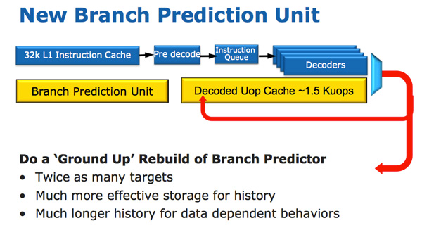
The CPU architecture of Sandy Bridge looks evolutionary with a brief overview, but it is revolutionary in terms of the number of transistors that have changed since the days of Nehalem / Westmere. The most important change for Sandy Bridge (and all microarchitectures after it) is the micro-operation cache (uOp cache).
A micro-operation cache appeared in Sandy Bridge, which caches instructions after they are decoded. There is no complicated algorithm, decoded instructions are simply saved. When the Sandy Bridge prefetcher receives a new instruction, it first searches for the instruction in the micro-operations cache, and if it is found, the rest of the pipeline will work with the cache, and the front end will be disabled. Decoding hardware is a very complex part of the x86 pipeline, and turning it off saves a significant amount of energy.
This is a direct mapping cache, and can store approximately 1.5 KB of micro-ops, which is actually equivalent to the 6 KB of instructions cache. The micro-op cache is included in the L1 instruction cache, and its Hit Rate for most applications reaches 80%. The micro-operation cache has a slightly higher and stable throughput compared to the instruction cache. The actual L1 command and data caches have not changed, they still constitute 32 KB each (64 KB L1 in total).
All instructions coming from the decoder can be cached by this mechanism, and, as I said, there are some special algorithms in it - simply, all instructions are cached. Long-unused data is deleted when space ends. A microoperational cache may seem similar to the tracing cache in Pentium 4, but with one significant difference: it does not cache traces. This is simply an instruction cache in which micro-operations are stored instead of macro-operations (x86 instructions).
Along with the new micro-cache, Intel also introduced a completely redesigned branch prediction module. The new BPU is about the same as its predecessor, but much more accurate. The increase in accuracy is the result of three major innovations.
The standard branch predictor is a 2-bit predictor. Each branch is marked in the table as accepted / not accepted with appropriate reliability (strong / weak). Intel found that almost all the branches predicted by this bimodal predictor have “high” confidence. Therefore, in Sandy Bridge, a bimodal branch predictor uses one confidence bit for multiple branches, rather than one confidence bit for each branch. As a result, your branch history table will be the same as before, the number of bits that represent many more branches, which leads to more accurate predictions in the future.
Sandy Bridge: near the core
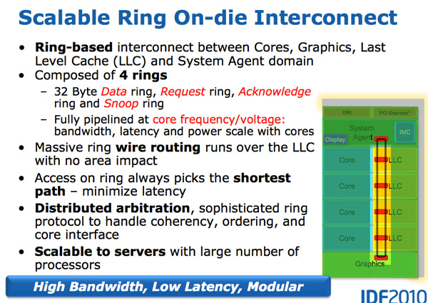
With the growth of multi-core processors, managing the flow of data between cores and memory has become an important topic. We have seen many different ways to move data around the CPU, such as crossbar (cross), ring (ring), mesh (mesh), and, later, completely separate I / O chips. The battle of the next decade (2020+), as mentioned earlier by AnandTech, will be a battle of inter-core connections, and now it is already beginning.
The feature of Sandy Bridge is that it was Intel's first consumer CPU, which used a ring bus connecting all the cores, memory, last-level cache, and integrated graphics. This is still the same design that we see in modern Coffee Lake processors.
Ring bus
In Nehalem / Westmery Bridge adds a graphics processor and video transcoding engine to the chip, which share the L3 cache. And instead of running more wires to the L3, Intel introduced the ring bus.
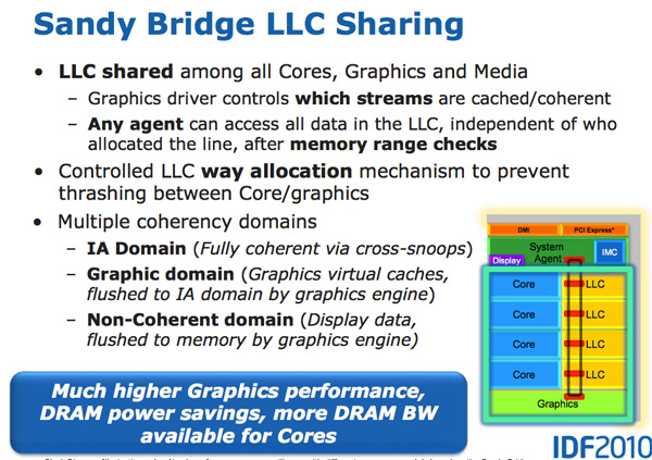
Architecturally, this is the same ring bus used in the Nehalem EX and Westmere EX. Each core, each fragment of the L3 cache (LLC), the integrated graphics processor, the media engine, and the system agent (a funny name for the north bridge) are attached to the ring bus. A bus consists of four independent rings: a data bus, requests, acknowledgments, and a state monitoring bus. Each call to any of the rings can transmit 32 bytes of data per clock. As the number of cores and the size of the cache increases, the throughput of your cache increases accordingly.
Each core in the end accounts for the same amount of L3 cache bandwidth as in high-performance Westmere processors — 96 GB / s. Sandy Bridge’s aggregate throughput is 4 times higher than the Westmere quad-core because it simply multiplies by the number of cores and is 384 GB / s.
This means that the L3 latency is significantly reduced from about 36 clocks in Westmere to 26 to 31 clocks in Sandy Bridge (with some variable cache delay, which depends on which core accesses which fragment of cache). In addition, unlike Westmere, the L3 cache now runs at the core clock — the un-Core concept still exists, but Intel calls the extra-core part the “system agent” and no longer includes the L3 cache. (The term "un-Core" is still used today to describe interconnects.)
Thanks to the L3 cache, which runs at the core frequency, you get the benefits of a much faster cache. The disadvantage is that L3 accelerates with the processor cores when turbo or idle modes are enabled. If the graphics processor needs L3, when the core frequency is lowered, the L3 cache will not work as fast as if it were independent. Or the system will have to overclock the core and consume additional power.
L3 cache is divided into fragments, each of which is associated with a separate core. Because Sandy Bridge has a fully accessible L3 cache, each core can address the entire cache. Each fragment has its own bus access controller, and a full cache pipeline. In Westmere, there was one cache pipeline and a queue to which all the kernels sent requests, but in Sandy Bridge they are distributed into cache segments. Using a ring bus means adding new access points to the bus has ceased to critically affect the size of the matrix. Despite the fact that each user of the ring receives its own controller, the data always follow the shortest path. Bus control is distributed throughout the ring, and as a result, each module “knows” whether the empty slot on the bus was one clock back.
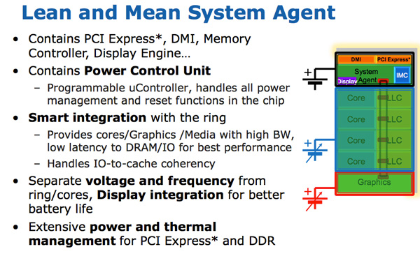
System agent
For some reason, Intel stopped using the un-core term in SB, and Sandy Bridge called this part “system agent”. (Again, un-core is now back in fashion for interconnects, I / O, and memory controllers). The system agent is a traditional North Bridge. You have 16 PCIe 2.0 lanes available, which can be divided into two x8 channels. There is a reworked dual-channel DDR3 memory controller, which finally provides memory latency at about Lynnfield (Clarkdale moved the memory controller from the CPU to the graphics processor).
The system agent also has a DMI interface, a video output unit and a PCU (power management unit). The clock frequency of SA is lower than that of the rest of the core, and has a separate power scheme.
Sandy Bridge Graphics
Another major performance improvement Sandy Bridge has in comparison to Westmere is graphics processing. While the processor cores show a performance improvement of 10-30%, Sandy Bridge's graphics performance is simply twice as high as that of Intel products before Westmere (Clarkdale / Arrandale). Despite the jump from 45 nm to 32 nm, the graphics processing speed improves due to a significant increase in IPC.
The Sandy Bridge GPU is built on the same 32nm transistors as the processor cores. The graphics processor is in its own little world in terms of power and frequency. The GPU can be turned off or on regardless of the processor. Graphic turbo is available for both desktop and mobile processors.
The GPU is treated as an equal citizen in the Sandy Bridge world, and gets full access to the L3 cache. The graphics driver controls what exactly gets into the L3 cache, and you can even limit the amount of cache that is available to the graphics processor. Storing graphics in the cache is especially important because it reduces recourse to main memory, which are costly both in terms of performance and in terms of power consumption. But rebuilding the graphics processor to use the cache is not an easy task.
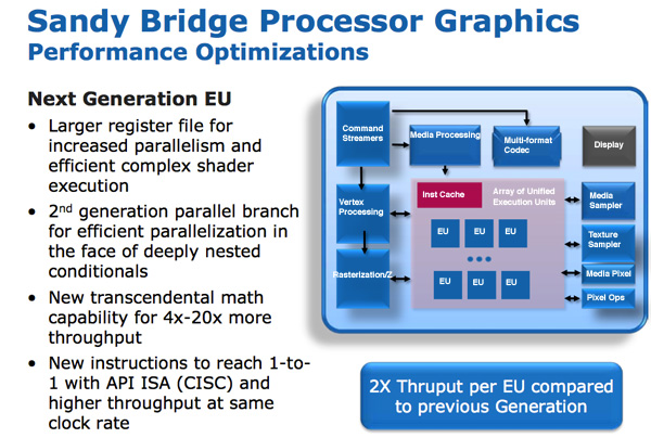
SNB graphics (internal name Gen 6) make extensive use of hardware with fixed functions. The idea is this: everything that can be described using a fixed function, which must be implemented by a hardware fixed function. The advantage is performance, power and reduced matrix size, albeit at the cost of loss of flexibility.
Programmable shader hardware consists of shaders / cores / execution units, which Intel calls the EU. Each EU can accept instructions from multiple threads. Internal ISA is mapped one-to-one to most DirectX 10 API instructions, meaning a CISC-like architecture. The transition from a one-to-one API to display instructions increases IPC by effectively increasing the width of the EU.
There are other improvements in the EU. Transcendental mathematics is processed by hardware in the EU, and its performance has increased significantly. Intel then reported that sine and cosine operations are now several orders of magnitude faster than in graphics to Westmere.
Intel's previous graphics architectures have been redistributed on the fly. If a stream requires fewer registers, the remaining registers can be allocated to another stream. Despite the fact that it was an excellent approach to save the area of the matrix, it turned out to be a performance limiter. Often the threads could not be processed because there were no registers available for use. Intel increased the number of registers per stream first from 64 to 80, and then to 120 for Sandy Bridge. Downtime scenarios due to a lack of registers have been significantly reduced.
In sum, all these improvements have doubled the throughput of instructions in the EU.
At launch, there were two versions of the Sandy Bridge GPU: one with 6 EU and one with 12 EU. All mobile processors (at startup) use 12 EU, while in desktop SKUs 6 or 12 can be used, depending on the model. Sandy Bridge was a step in the right direction for Intel, as integrated graphics began to become mandatory for consumer products, and Intel gradually began to increase the percentage of chip space allocated to the GPU. Modern (2019) desktop processors of a similar level have 24 EU (Gen 9.5), while future 10-nm processors will have ~ 64 EU (Gen11).
Sandy bridge media engine
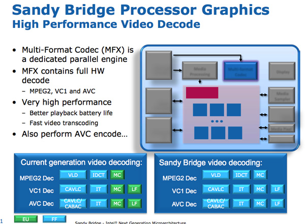
Next to the Sandy Bridge GPU is a media processor. SNB media processing consists of two main components: video decoding and video encoding.
The hardware accelerated decoding mechanism has been improved compared to the current generation: now the entire video pipeline has been decoded using modules with fixed functions. This contrasts with Intel's pre-SNB design, which uses an EU array for some video decoding stages. As a result, Intel claims that the power consumption of the SNB processor is halved when playing HD video.
The video encoding engine was a completely new addition to Sandy Bridge. Intel took a ~ 3-minute original 1080p 30 Mbit / s video and recoded it into an iPhone 640 x 360 video format. The whole process took 14 seconds and ended at about 400 frames per second.
The principle of encoding / decoding by a fixed function is now common in any graphics hardware for desktops and even smartphones. At that time, Sandy Bridge used 3 mm2 matrices for this basic encoding / decoding structure.
New, Aggressive Turbo
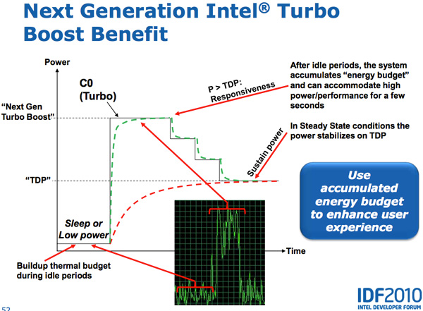
Lynnfield Intel, . , TDP 95 , , , -.
, - . , , — , .
Sandy Bridge , PCU TDP ( 25 ). PCU , . , , TDP. , , TDP, , , TDP. SNB TDP, PCU .
Both CPU and GPU Turbo can work in tandem. Workloads that are more related to GPUs running on SNBs can lead to lower CPU core frequencies and higher GPU frequencies. Also, tasks related to the CPU can reduce the frequency of the GPU and increase the frequency of the CPU. Sandy Bridge as a whole turned out to be a much more flexible mechanism than anything that was created before it.
Thank you for staying with us. Do you like our articles? Want to see more interesting materials? Support us by placing an order or recommending to friends, 30% discount for Habr's users on a unique analogue of the entry-level servers that we invented for you: The Truth About VPS (KVM) E5-2650 v4 (6 Cores) 10GB DDR4 240GB SSD 1Gbps $ 20 or how to share the server? (Options are available with RAID1 and RAID10, up to 24 cores and up to 40GB DDR4).
Dell R730xd 2 times cheaper? Only we have 2 x Intel TetraDeca-Core Xeon 2x E5-2697v3 2.6GHz 14C 64GB DDR4 4x960GB SSD 1Gbps 100 TV from $ 199 in the Netherlands! Dell R420 - 2x E5-2430 2.2Ghz 6C 128GB DDR3 2x960GB SSD 1Gbps 100TB - from $ 99! Read about How to build an infrastructure building. class c using servers Dell R730xd E5-2650 v4 worth 9000 euros for a penny?
Source: https://habr.com/ru/post/455610/
All Articles