Developing your own core for embedding into the FPGA processor system
So, in the first article of the cycle, it was said that for controlling the equipment implemented by the FPGA, for the Redd complex it is best to use the processor system, after which during the first and second articles it was shown how to do this system. Well, it is done, we can even select some ready-made kernels from the list to include them in it, but the ultimate goal is to manage our own non-standard kernels. It is time to consider how to include an arbitrary core in the processor system.
All articles of the cycle:
Development of the simplest “firmware” for the FPGA installed in Redd, and debugging using the memory test as an example
Development of the simplest “firmware” for the FPGA installed in Redd. Part 2. Program Code
To understand today's theory, you should find and download the Avalon Interface Specifications document, since the base bus for the NIOS II system is the Avalon bus. I will refer to sections, tables and figures for the wording of the document dated September 26, 2018.
')
We open section 3, devoted Memory Mapped Interfaces, to be exact - 3.2. Table 9 lists the bus signals. Note that all of these signals are optional. I did not find a single signal that had “Yes” in the Required column. We may well not to send one or another signal to our device. Therefore, in the simplest case, the tire is extremely easy to implement. The beginning of the table looks like this:

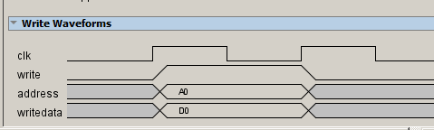
As you can see, all the signals are very well described (unless it is done in English). Below are timing charts for various cases. The simplest case does not cause any questions. I will now take a temporary diagram from the document and cover some of the lines with a semitransparent fill (they are all optional, we have the right to exclude any consideration).
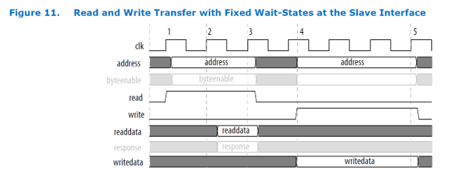
Fearfully? But it's simple: we put the address and the strobe read , we must put the data on the readdata bus. And vice versa: we are given the address, the data on the writedata bus and the write strobe, and we have to snap the data. It is not scary at all, a typical tire synchronous.
Covered byteenable lines are needed for the case when memory access is not in 32-bit words. This is extremely important when we design generic kernels. But when we design a one-day kernel, then we simply write in the document about this core (I am opposed to the mark in my head, but someone can limit it to this) that you need to apply 32-bit words and that's it. Well, the response signal, it is very special, and it does not interest us in principle.
Sometimes it is important that when the equipment is not ready, it is possible to delay the operation of the bus for several cycles. In this case, add the WaitRequest signal. The timing diagram changes as follows:
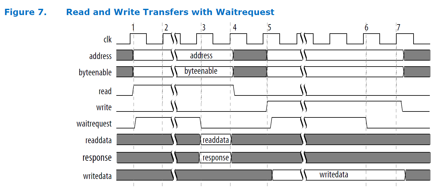
While WaitRequest is cocked, the master knows that our device is busy. Be careful, if this signal is not reset, the whole system will “hang” when it is accessed, so that only a reset of the FPGA can reset it. JTAG will hang with the system. The last time I saw this phenomenon in the preparation of this article, so that the memories are still bright.
Further in the company document, more productive cases of data pipelining and batch transactions are considered, but the task of the article is not to consider all possible options, but to show the reader a way to work, emphasizing that all this is not at all scary, so we limit ourselves to these two simple options.
Let's design some simple device that will periodically become unavailable via the bus. The first thing that comes to mind is the serial interface. While we are transmitting, we will make the system wait. And in life, I categorically do not advise doing this: the processor will stop until the end of a busy transaction, but for an article this is an ideal case, since the implementing code will be understandable and not very cumbersome. In general, we will make a serial transmitter that can send data and signals for selecting a chip to two devices.
Let's start with the simplest version of the tire. We make a parallel output port, which forms the signals for selecting crystals.
To do this, I will take the project, which turned out in the last article, but in order to avoid confusion, I will put it in the AVALON_DEMO catalog. The names of other files will not change. In this directory, create the directory my_cores . The directory name can be any. We will store our cores in it. True, today it will be one. We create a file there CrazySerial.sv with the following contents:
module CrazySerial ( input clk, input reset, input [1:0] address, input write, input [31:0] writedata, output reg [1:0] cs ); always @(posedge clk, posedge reset) begin if (reset == 1) begin cs <= 0; end else begin if (write) case (address) 2'h00: cs <= writedata [1:0]; default:; endcase end end endmodule Let's figure it out. First of all, the interface lines. clk and reset are clocking and reset lines. The names of the lines address , write and writedata are taken from the table with the list of signals Memory Mapped Interfaces of the document.

In fact, the names I could give any. The linking of logical lines with physical ones will be made later. But if you give the names as in the table, the development environment will link them themselves. Therefore, it is better to take the names from the table.
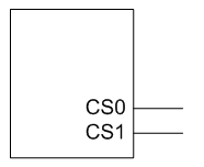
Well, and cs are the crystal selection lines that will come out of the chip.
The implementation itself is trivial. When reset, the outputs are zeroed out. And so - on each clock cycle we check if there is a write signal. If the address is zero, then click the data. You could, of course, add a decoder here, which would prevent the choice of two devices at once, but what is good in life will overload the article. The article provides only the most necessary steps, however, it is noted that in life everything can be done and more complicated.
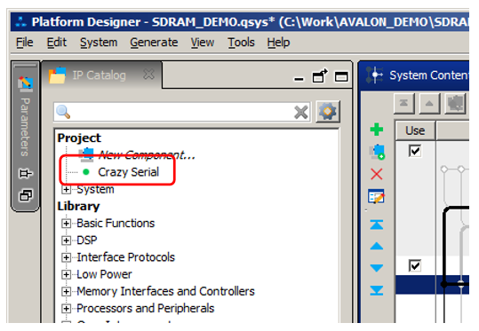
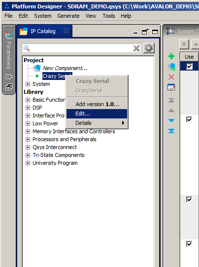
Perfectly. We are ready to inject this code into the processor system. Go to the Platform Designer , select the system that we built during past experiences as an input file:
Pay attention to the New Component item in the upper left corner:

To add your component, click on this item. In the opened dialog we fill the fields. And for the article we will fill in only the name of the component:

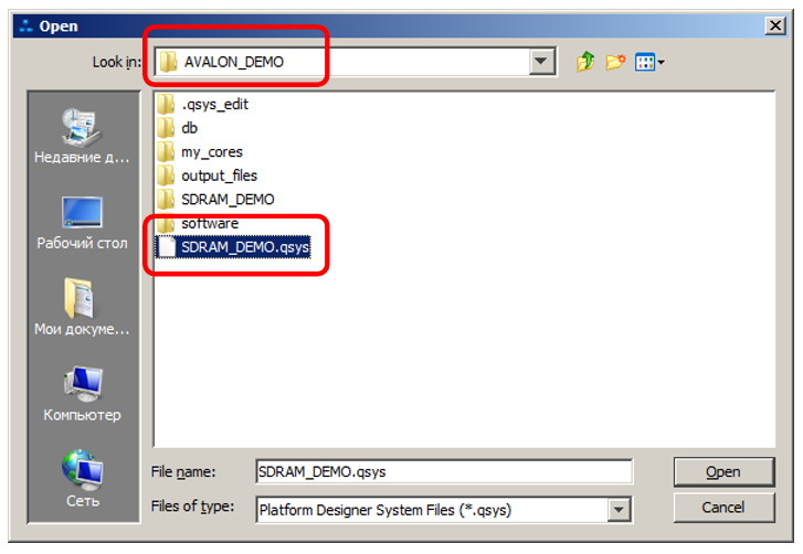
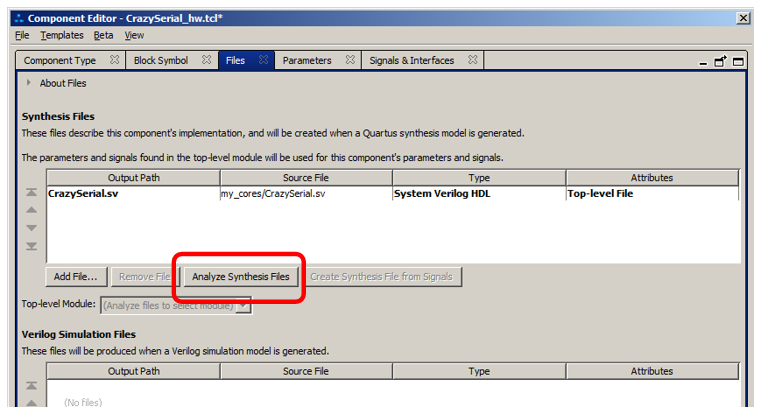
Now go to the Files tab and click Add File :
Add a previously created file, select it in the list and click Analyze Synthesis File :
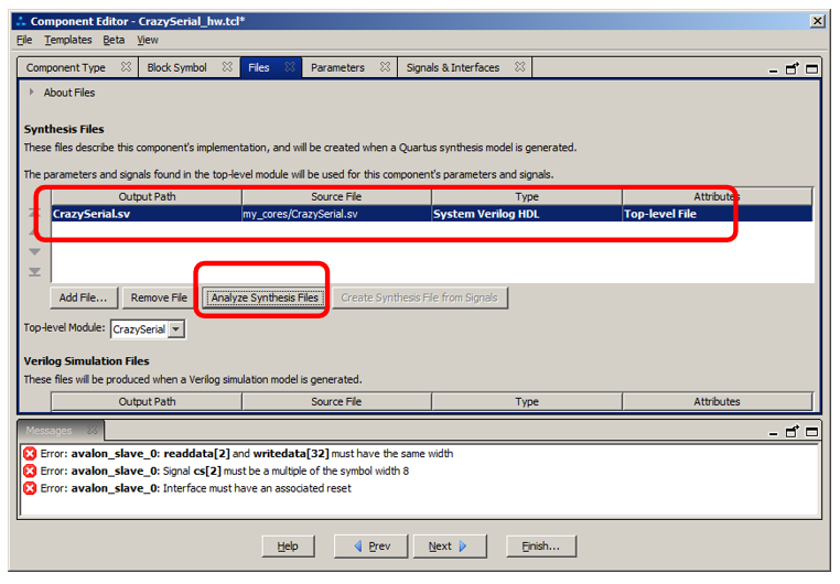
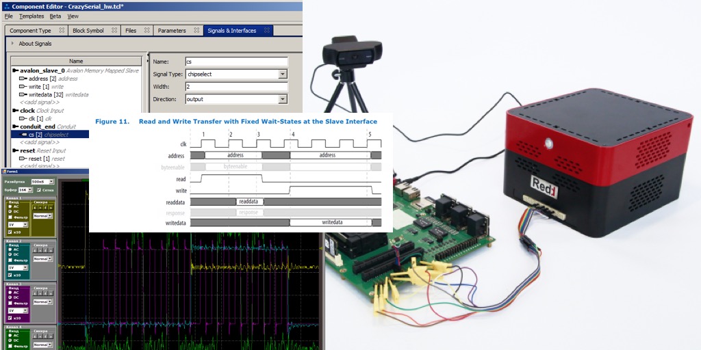
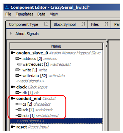
There are no errors when parsing SystemVerilog , but there are a few conceptual errors. They are caused by the fact that some lines were incorrectly connected by the development environment. Go to the Signals & Interfaces tab and pay attention here:
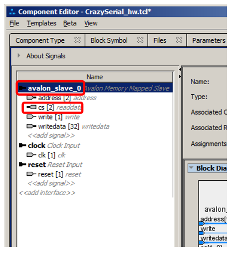
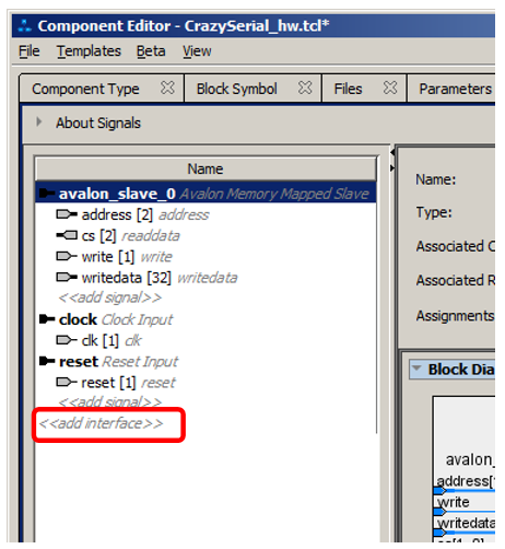
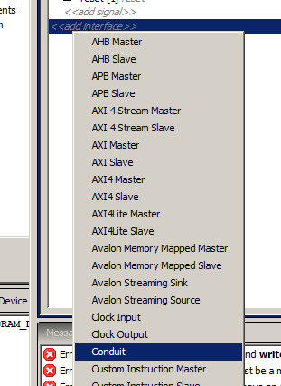
The cs lines were incorrectly assigned to the avalon_slave0 interface, the readdata signal. But all the other lines were recognized correctly, thanks to the fact that we gave them the names from the document table. But what to do with the problem lines? They should be attributed to the interface type conduit . To do this, click on the item "add interface"
In the popup menu, choose conduit :
We get a new interface:
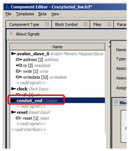
If you wish, you can rename it. True, it will certainly be necessary if we want to make several external interfaces. As part of the article, let's leave him the name conduit_end Now we grab the cs line with a mouse and drag it into this interface. We need to manage to throw a signal under the line conduit_end , then we will be allowed to do this. In other places the cursor will be displayed in the form of a crossed circle. In the end, we should have this:
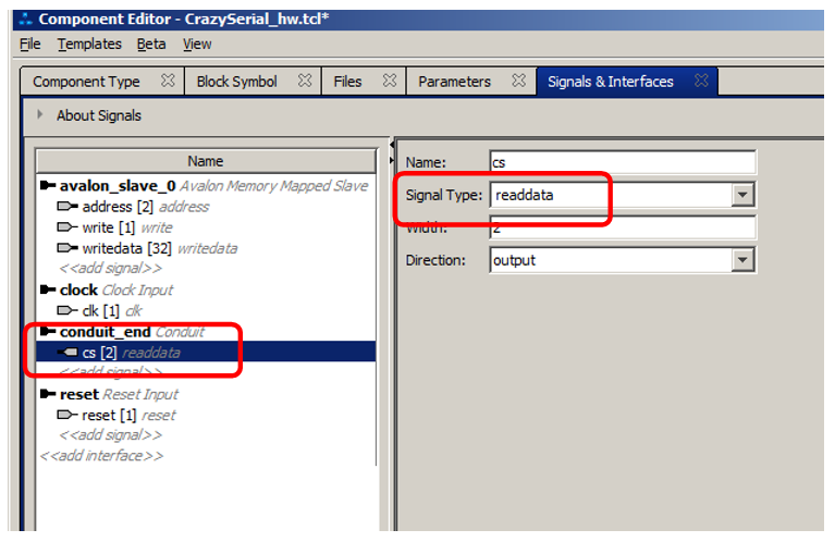
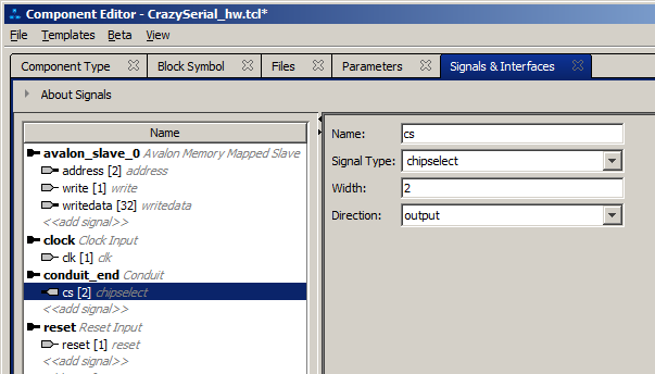
Replace the type of signal from readdata to, say, chipselect . The final picture:
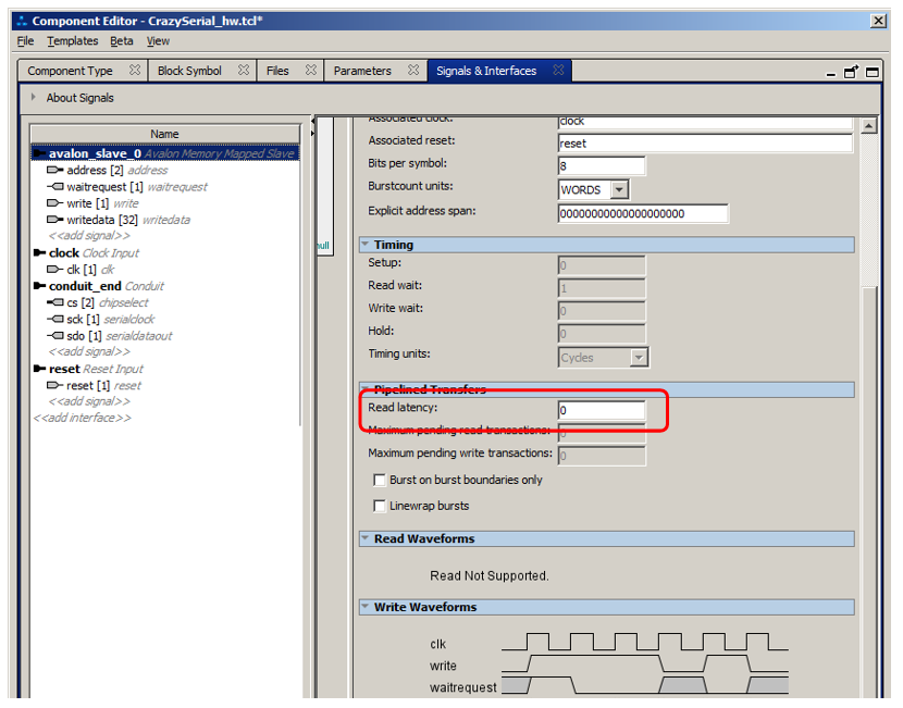
But the mistakes remained. The avalon bus is not assigned a reset signal. Select avalon_slave_0 from the list and see its properties.

Replace none with reset . At the same time examine the other properties of the interface.
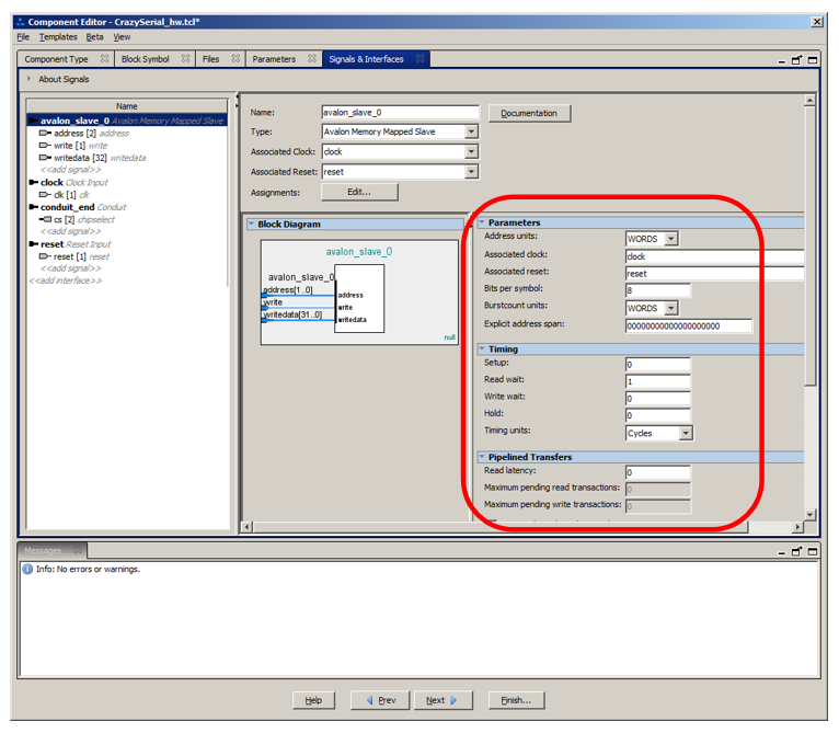
It can be seen that the addressing is in words. Well, a number of other things from the documentation is configured here. What time schedules will be obtained will be drawn at the very bottom of the properties:
Actually, there are no more errors. You can click Finish . Our created module appeared in the device tree:
Add it to the processor system, connect the clock signals and reset. We connect the data bus to the processor's Data Master . Double-click on Conduit_end and give the external signal a name, say, lines . It turns out something like this:

It is important here not to forget that since we have added a block to the system, we must make sure that it does not conflict with anyone in the address space. In this particular case, there are no conflicts in the figure, but still I will select the System-> Assign Base Addresses menu item .
Everything. The block is created, configured, added to the system. Press the button Generate HDL , then - Finish .
We make a draft assembly of the project, after which we go to Pin Planner and assign the legs. I did this:

That corresponds to pins B22 and C22 of the interface connector.
We make a final assembly, we load the processor system into the FPGA. Now we need to refine the program code. Run Eclipse.
Let me remind you, I am currently working with a project that is located in another directory regarding my previous work with Redd. In order not to be confused, I will delete old projects from the tree (but only from the tree, without erasing the files themselves).

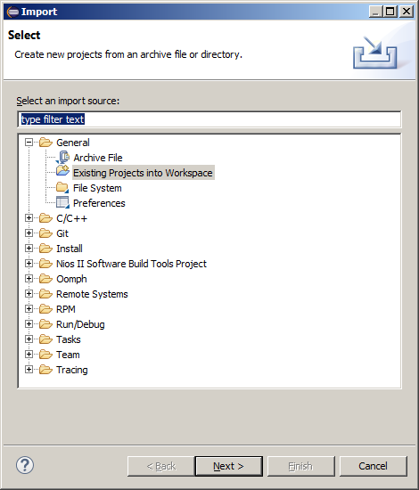
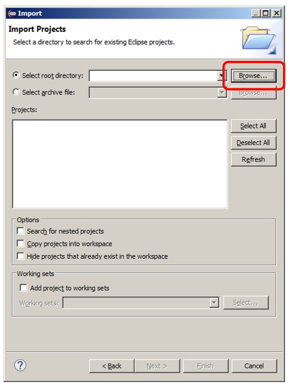
Then click the right mouse button on the empty tree and select Import in the menu:
Next - General-> Existing Project into Workspace :
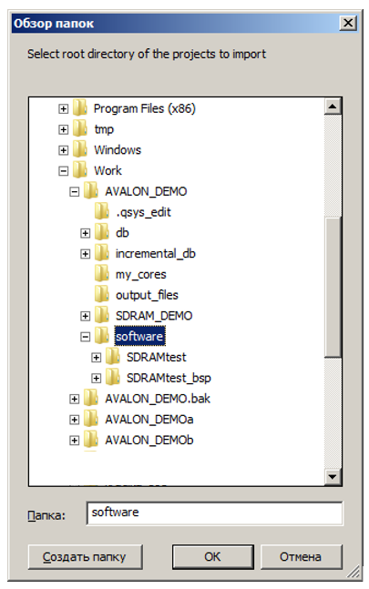
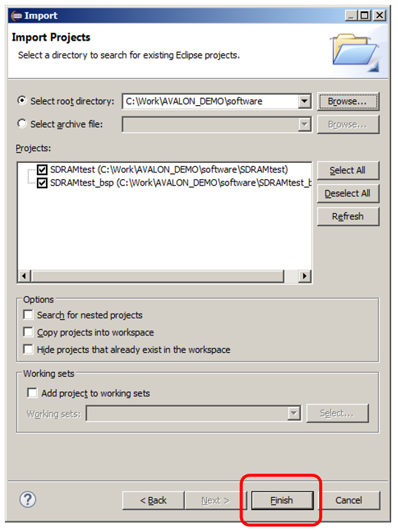
And just choose the directory in which the project files are stored:
Both projects inherited from past experiments will connect to the development environment.
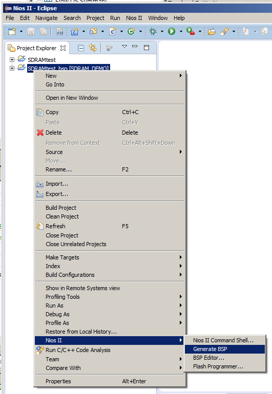
I will highlight the next item in the frame:
Each time after changing the hardware configuration, you should re-select the menu item Nios II -> Generate BSP for the BSP project.
Actually, after this operation, a new block appeared in the file \ AVALON_DEMO \ software \ SDRAMtest_bsp \ system.h :
/* * CrazySerial_0 configuration * */ #define ALT_MODULE_CLASS_CrazySerial_0 CrazySerial #define CRAZYSERIAL_0_BASE 0x4011020 #define CRAZYSERIAL_0_IRQ -1 #define CRAZYSERIAL_0_IRQ_INTERRUPT_CONTROLLER_ID -1 #define CRAZYSERIAL_0_NAME "/dev/CrazySerial_0" #define CRAZYSERIAL_0_SPAN 16 #define CRAZYSERIAL_0_TYPE "CrazySerial" We are primarily interested in the constant CRAZYSERIAL_0_BASE .
Add the following code to the main () function:
while (true) { IOWR_ALTERA_AVALON_PIO_DATA (CRAZYSERIAL_0_BASE,0x00); IOWR_ALTERA_AVALON_PIO_DATA (CRAZYSERIAL_0_BASE,0x01); IOWR_ALTERA_AVALON_PIO_DATA (CRAZYSERIAL_0_BASE,0x02); IOWR_ALTERA_AVALON_PIO_DATA (CRAZYSERIAL_0_BASE,0x03); } We start debugging and watch the contents of the lines with an oscilloscope. Must be an incremental binary code. He is there.
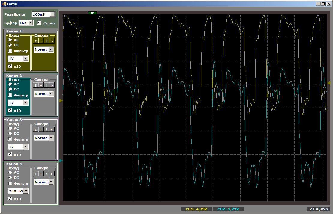
And the frequency of access to the ports is just wonderful:
Approximately 25 MHz is half the bus frequency (2 clocks per cycle). Sometimes the access time is not 2 cycles, but more. This is due to the execution of branch operations in the program. In general, the simplest access to the bus works.
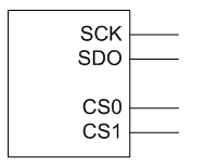
The time has come to add to the example the functionality of the serial port. To do this, add the waitrequest interface signal related to the bus and a couple of signals of the serial port - sck and sdo . So, we get the following code snippet on systemverilog :

Same text:
module CrazySerial ( input clk, input reset, input [1:0] address, input write, input [31:0] writedata, output waitrequest, output reg [1:0] cs, output reg sck, output sdo ); According to the rules of good tone, you need to make an uncomplicated machine that will transfer data. Unfortunately, the most simple machine within the article will look very difficult. But in fact, if I do not increase the functionality of the machine (and in the framework of the article I’m not going to do this), then it will have only two states: the transmission is on and there is no transmission. Therefore, I can encode the state with one signal:
reg sending = 0;
During the transfer, I will need a bit counter, a clock divider (I also make a deliberately slow device) and a shift register for the transmitted data. Add the appropriate registers:
reg [2:0] bit_cnt = 0; reg [3:0] clk_div = 0; reg [7:0] shifter = 0; I will divide the frequency by 10 (guided by the principle “why not?”). Accordingly, on the fifth cycle I will cock SCK, and on the tenth - drop this line, after which - carry out the transition to the next bit of data. On all other bars, simply increment the divisor counter. It is important not to forget that on the fourth clock cycle it is also necessary to increase the counter, and on the ninth one to zero it. If you omit the process of moving to the next bit, then the specified logic looks like this:
if (sending) begin case (clk_div) 4: begin sck <= 1; clk_div <= clk_div + 1; end 9: begin sck <= 0; clk_div <= 0; // < > end default: clk_div <= clk_div + 1; endcase end else The transition to the next bit is simple. Shifted shift register, then, if the current bit is the seventh, stopped working, switching the state of the machine, otherwise - increased the bit counter.
shifter <= {shifter[6:0],1'b0}; if (bit_cnt == 7) begin sending <= 0; end else begin bit_cnt <= bit_cnt + 1; end Actually, everything. The output bit is always taken from the high bit of the shift register:
assign sdo = shifter [7]; And the most important line for the current revision. Signal waitrequest we cock in unit always, when there is a transfer of consecutive data. That is, it is a copy of the sending signal that sets the state of the machine:
assign waitrequest = sending; Well, when writing to address 1 (remember, here we have the addressing in 32-bit words), we snap the data into the shift register, reset the counters and start the transfer process:
if (write) //... 2'h01: begin bit_cnt <= 0; clk_div <= 0; sending <= 1; shifter <= writedata [7:0]; end default:; endcase end Now I will give all the described fragments in the form of a single text:
module CrazySerial ( input clk, input reset, input [1:0] address, input write, input [31:0] writedata, output waitrequest, output reg [1:0] cs, output reg sck, output sdo ); reg sending = 0; reg [2:0] bit_cnt = 0; reg [3:0] clk_div = 0; reg [7:0] shifter = 0; always @(posedge clk, posedge reset) begin if (reset == 1) begin cs <= 0; sck <= 0; sending <= 0; end else begin if (sending) begin case (clk_div) 4: begin sck <= 1; clk_div <= clk_div + 1; end 9: begin clk_div <= 0; shifter <= {shifter[6:0],1'b0}; sck <= 0; if (bit_cnt == 7) begin sending <= 0; end else begin bit_cnt <= bit_cnt + 1; end end default: clk_div <= clk_div + 1; endcase end else if (write) case (address) 2'h00: cs <= writedata [1:0]; 2'h01: begin bit_cnt <= 0; clk_div <= 0; sending <= 1; shifter <= writedata [7:0]; end default:; endcase end end assign sdo = shifter [7]; assign waitrequest = sending; endmodule We begin to introduce a new code into the system. Actually, the path is the same as when creating the component, but some of the steps can already be omitted. Now we just get to know the process of refinement. Go to the Platform Designer . If we had only verilog code exchanged, it would be enough to simply perform the Generate HDL operation for the finished system. But since the module has new lines (that is, the interface has changed), it needs to be redone. To do this, select it in the tree, press the right mouse button and select Edit .
We are editing a ready-made system. So just go to the Files tab and click Analyze Sinthesis Files :
Predictably errors occurred. But we already know that the blame for all the misinterpreted lines. Therefore, we go to the Signals & Interfaces tab, drag along the sck and sdo lines from the avalon_slave_0 interface to the conduit_end interface:

Also rename the Signal Type fields for them. The result should be the following:
Actually, everything. Click Finish , call Generate HDL File for the processor system, do the draft build of the project in Quartus, assign the new legs:
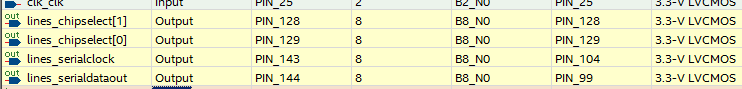
These are contacts A21 and A22 of the interface connector, we are doing the final assembly, we fill in the “firmware” in the FPGA.
Iron updated. Now - the program. Go to Eclipse. What we do not forget to do there? That's right, do not forget to choose Generate BSP .
Actually, everything. It remains to add functionality to the program. We will send a pair of bytes to the serial port, but send the first byte to the device selected by the cs [0] line , and the second by cs [1] .
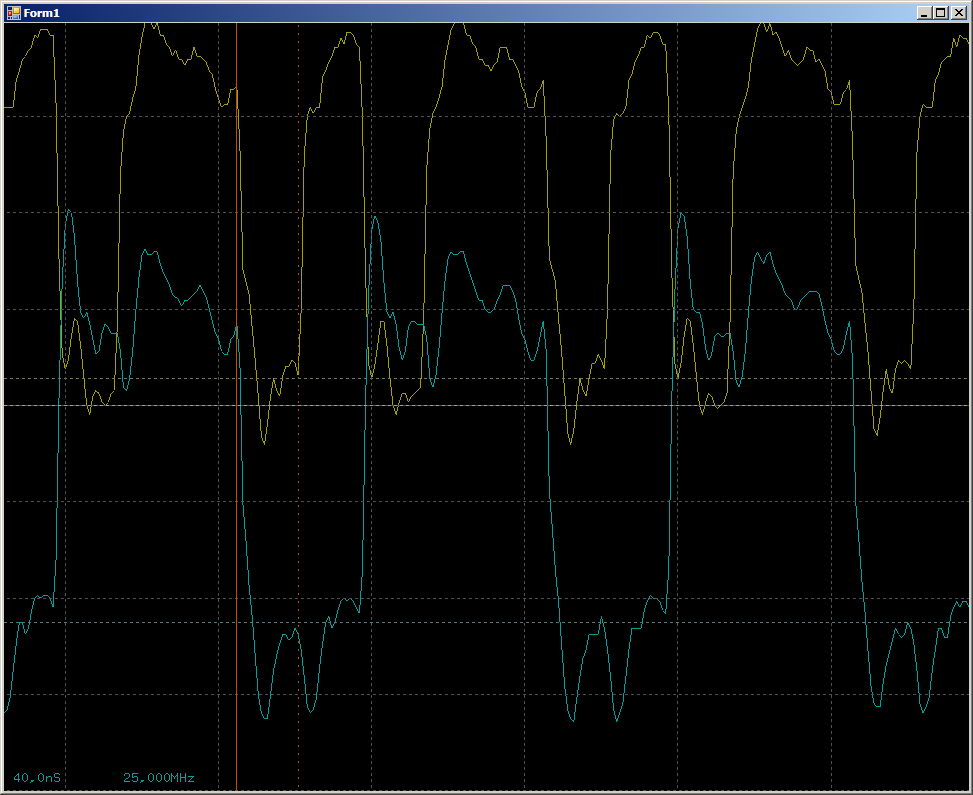
IOWR_ALTERA_AVALON_PIO_DATA (CRAZYSERIAL_0_BASE,0x01); IOWR_ALTERA_AVALON_PIO_DATA (CRAZYSERIAL_0_BASE+4,0x12); IOWR_ALTERA_AVALON_PIO_DATA (CRAZYSERIAL_0_BASE,0x02); IOWR_ALTERA_AVALON_PIO_DATA (CRAZYSERIAL_0_BASE+4,0x34); IOWR_ALTERA_AVALON_PIO_DATA (CRAZYSERIAL_0_BASE,0x00); Please note that there are no readiness checks. Parcels go one after another. However, everything on the oscilloscope was quite consistent.
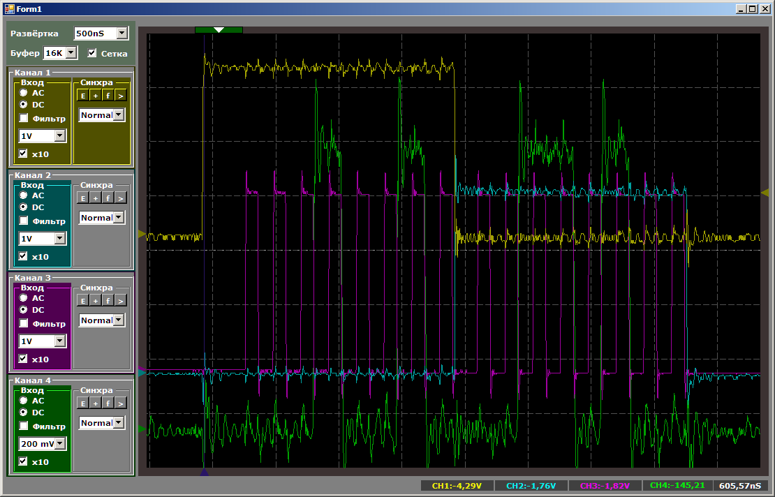
The yellow beam is cs [0] , the green is sdo , the purple is sck , the blue is cs [1] . It can be seen that the code 0x12 went to the first device, 0x34 went to the second one.
Reading is done in a similar way, but I just can’t think of any beautiful example, apart from the banal reading of the contents of the connector foot. But that example is so degenerate that it is not even interesting to do it. But here it is worth noting that when reading this bus setting can be extremely important:
If there is a line Read , then a time diagram of reading will appear on the settings dialog. And it will show the effect of this parameter. When reading the connector leg, it will still not be noticeable, but when reading from the same FIFO or RAM - completely. RAM can be configured to issue data immediately after the address is submitted, or it can be sent to synchronous output. In the second case, latency is added. After all, the bus set the address, set the gate ... But there is no data yet on the nearest edge of the clock signal. They will appear after this front ... That is, the system has latency in one clock cycle. And just it is necessary to consider it, having set this parameter. In short, if it’s not what was expected, first check to see if you need to adjust latency. As for the rest, reading is no different from writing.
Well, let me remind you once again that it is better not to remove the tire readiness during long operations, otherwise it is quite possible to drastically reduce system performance. The readiness signal is good to hold the transaction for a couple of ticks, and not up to 80 ticks, as in my example. But firstly, any other example would be inconvenient for an article, and secondly, for one-day kernels, this is completely acceptable. You will be fully aware of your actions and will avoid situations where the tire is blocked. However, if the core survives the time allotted to it, such an assumption can ruin life in the future, when everyone will forget about it, but it will slow down everything. But it will be later.
Nevertheless, we have learned how to make the processor core control our cores. With the addressed world everything is clear, now it’s time to deal with the streaming world. But we will do this in the next article, and perhaps even a few articles.
Conclusion
The article shows how an arbitrary kernel in the Verilog language can be connected to control the means of the Nios II processor system. The options for the simplest connection to the Avalon bus are shown, as well as connections in which the bus can be in a busy state. There are links to literature, from which you can find other modes of the Avalon bus in Memory Mapped mode.
The resulting project can be downloaded here .
Source: https://habr.com/ru/post/454938/
All Articles