PDA (Pocket Travel Computer): GPS Logger Circuitry
My hobby project is GPS logger . In the comments they even suggested calling it “Travel Computer”, since logging is only a small part of all device capabilities. Much has already been implemented, but much of it remains to be done.
In previous articles, I described the transition from arduino to STM32 , STMCube / HAL , talked a little about the build system , bootloader , built a composite USB device and pumped its speed . All this was done on a breadboard based on a Blue Pill STM32F103CB board and a hedgehog made from wires. It is time for the device to take shape, both electronic (circuit) and physical (body).
')
The issues that I had to solve at this stage are very interrelated. Choosing the components for the project you need to roughly represent in which body they can be shoved. Conversely, the body must be made for the components that are available and the board, which, again, must be done with an eye to the body. In general, a tangle of interrelated issues. You can, of course, take a bigger box and push anything there, but you want something compact and light.
Before I start right away, I want to note that this is not the final version of the device. Most likely, there will be errors in the scheme, something will not work as planned, they will indicate more correct solutions in the comments, some approaches will be rethought. I think that the second or even the third version of the device can not be avoided. Therefore, I will be glad to your constructive comments.
Under the cat mnogabukav, but it will be interesting.
The Holux M241 GPS logger is my faithful companion on all trips. He is with me for many thousands of kilometers. The track that the logger writes is primarily used for geotagging photos, but the route itself is also of interest. It's fun to find out how fast you went skiing, which route your plane flew, what sight just flashed past the bus window. Here I did a little review of this device.
Unfortunately, the capabilities of this device have long ceased to suit me: tired of fiddling with batteries, which always sit at the most inopportune moment. Also, a very small USB speed, a small amount of internal flash, an inconvenient mechanism for merging tracks, little information is available on the display, little accuracy, a very primitive odometer, no information about satellites, and a lot more on the little things.
Yes, it would be possible to look for what modern trackers offer - for sure there is already a device on sale that meets my requirements. But this is a hobby, I want to try myself to do something complicated, interesting, useful and necessary. Let it be even if I will be the only one to use it.
The goal of the project as a whole is to make a similar device in something, only stuffed with my Wishlist. In the first article of the cycle, I described in detail my device requirements. In short, I would like to do the following:
In addition to technical requirements and there is also a non-technical hotelok (non-functional). So I would like to improve the creation of complex devices from scratch, to understand how various electronic components work, how to program them, how to make a motherboard and design a case.
Why do you need a separate device if all modern phones have GPS, a big screen and a lot of memory? Well, first of all, I'm not sure that a phone with GPS enabled in track recording mode can withstand the whole day. I would not really like to stay in an unfamiliar country without a phone. Also, I personally use a separate device simply more comfortable.
Perhaps over time, the concept of the device will change. So, for example, now the idea of abandoning the screen and connecting to the phone via bluetooth is becoming more and more logical, and doing all the tricky logic already in the phone. This idea is very sensible and tempting. But at this stage, I would still like to have a display - I always have time to give it up.
For the first year and a half, I developed a device on various debugging boards (first arduino nano, then STM32F103 blue pill, then STM32F407VE). It was necessary to connect the periphery on postings and purchased modules. As a result, a hedgehog from the wires was obtained on the table, which could not be tested on the GPS reception; it was impossible to even move the wires without breaking the connection somewhere. And then happy debugging.
Every time I sat down to write useful functionality, I rested on the fact that some other part of the system stopped working normally and I had to spend hours debugging something completely unrelated. For example, the most important component of the system, the GPS receiver, turned out to be the least developed, since I had to go headlong into debugging USB, SD cards, setting up libraries and such.
Finally I got tired of it and I decided to make my debug board - this will be the topic of today's article. The goals that I set myself in this part of the project were:
And although the ultimate goal is a compact battery device, today I will not do such things as
I will deal with the consumption setting when the board and the main code are ready. By the way, about the code today, too, will not, but I will definitely return to this issue as there will be quite interesting material.
Let's start with the components and peripherals. On the way, let us estimate the number of microcontroller legs that will be needed to connect this zoo, as well as the power options. Because This is a hobby project, that I chose the components from the fact that I really bought in the shops / ebay / ali, as well as the fact that you can solder at home (well, and also from what was already in personal stocks). Perhaps some specific chips could solve the problem better, but the issue of accessibility and price is important to me.
I was always interested in the question of why we need controllers with a large number of ports, and I myself easily counted 39 paws needed for my functionality. And that's not counting quartz, reset, and power. And there are ideas about what to do with a dozen more (for example, the display could be connected via a parallel interface of the Intel 8080 or Motorola 6800).
You can, of course, fasten the I2C port externders to reduce the number of feet used. But firstly, these are additional components on the board, secondly, the software part is very complicated, and thirdly, there is still little memory in small microcontrollers, and where there is enough memory, there are also enough ports. So I do not see the point of complicating everything - let it be 39 lines.
With the supply voltage is not so clear. You can probably power all devices from 3.3V and calm down on this. But we, all the same, are going to do a mobile device, which means we need to think about saving energy. So you need to try to choose a smaller supply voltage. Below, I will figure out what kind of savings you can try to achieve.
Here is the data for all devices on the plate - in this form it is more convenient to choose the power domain to which to connect this or that device.
From the plate it is easy to see that some devices can operate on sufficiently low voltages (from 1.8V). Others can comfortably work from 2.7V. Finally, the remaining devices below 3V cannot work. A squeaker, for good, generally needs 5V, but for me it will be powered by the highest voltage - from the battery, no matter how much it is.
With the power of the display is not yet fully understood. In the description of display modules with ali, a range of 3 - 5V is indicated, whereas in the datasheet on the matrix controller SSD1309 a range of 1.65 - 3.3V is indicated. I assume that 3V is needed to shake the boost converter on the display module board, whereas logic is 1.65V. As will be seen from the reasoning about the layout, it makes sense to abandon the display module and connect the display directly, which will power the display from domain 2B.
I have about the same reasoning about GPS - different sources indicate different supply voltages. So far I have no idea which module I will use as a result, so let the receiver talk in the domain 2.7B.
With an SD card is not at all clear. The specification says dimly that, in general, the card should be powered from 3.3V, but modern cards are smart enough and can understand that they have been plugged into a low-voltage device and can switch to 1.8V. But the mechanism of food selection is not very clear. I will power the card from 2B and see what happens. It will not work - it will work from 3B.
So, 4 power buses emerge - 2V, 2.7V, 3V and a battery. I would like to put all the hungry and constantly working consumers (and this is the controller and GPS) onto the lowest volt bus, but at the moment I have not yet decided on the GPS module (and therefore its power supply - 2 or 2.7V), which means it will be necessary some kind of universal solution. I will try to dissolve the board so that it is easy to apply either one or the other.
Where do we get so many different voltages? Even in the early stages of the project, I looked at the PT1502 microcircuit even managed to try it in another project . In addition to charging for a lithium battery in this chip, there are already 3 power sources - one pulse and 2 linear lowers. True, on one of them the voltage is not regulated and amounts to 3V - I will try to power the INA219 from it. The remaining 2 power sources are not a problem, because there voltage can be chosen.
Estimate consumption is not very successful. The datasheets indicate peak consumption - this is enough to calculate the power of the key transistors, but not enough to estimate the required battery capacity. So while the battery will be selected on the basis of available space in the case, and there I’ll measure the actual consumption.
The question may arise, but how to co-ordinate devices with different operating voltages? Let's figure it out.
Finally, a few words about why I am so struggling to lower the supply voltage. The chip in a pulsed DC-DC converter that can exchange volts for amps (if you do not take into account the loss of the converter itself, of course). To be more precise, exchange higher voltage with low current for low voltage and higher current. In this case, we are more interested in reverse reasoning - if we power the low-voltage load through DC-DC, then the consumed current of this entire structure together with the converter will be lower than the consumed current of the load itself. Well, since battery capacity is measured in mAh, a decrease in current consumption will lead to an increase in battery life.
I approached the question of choosing a microcontroller thoughtfully - I played for a long time with the configurator, weighing all the pros and cons of each of the options. I really liked the STM32 microcontrollers, so I don’t see any point in looking towards other controllers without much need. Moreover, the STM32 line has controllers for every taste and for any periphery. The experience gained in the previous stages of my project allows us to narrow down the choice of controller based on the list of peripherals, the software already written, and the features that I would like to realize in the future.
So, it’s absolutely obvious that 20kb of my memory of my STM32F103CB is definitely not enough - there are not enough decent-sized buffers for communication between an SD card and USB. I haven't even started implementing much of the conceived functionality yet, and more than 19k are already taken. But with the power for processing, as it turned out, it is not particularly necessary. If all communication with the periphery is pushed into the DMA, then the share of the central processor remains only a couple of percent.
Having estimated the list of what I need from the controller, I counted the following:
STMicroelectornics microcontrollers are just a dime a dozen for every taste, color and wallet. At first I tried to proceed from the series when choosing a controller. The L0 and F0 lines are too weak and little memory, S7 and H7, on the contrary, are too sophisticated, L4 does not have SDIO (UPD: SDIO is, they just did not mention it on the title page of the series). Among the rest of the series, you can choose something based on my needs, since I have no particularly specific requirements.
The STM32WB series impresses with the presence of Bluetooth, but the VFQFPN68 case somewhat cools the desire to use it in hobby projects. And I did not find such controllers in retail.
I aimed at the body of the LQFP64 - sufficient for the number of legs, but it is not very big and can be soldered at home. It's good that there is a CubeMX configurator in which you can choose what you need by filters.
I chose the STM32F103RB controller for three reasons. Firstly, I have already studied the F103 series well using the example of the Blue Pill board. In general, the STM32F103CB controller completely suited me, but the memory was not enough. Secondly, I already have a bootloader and low-level code for this controller, while others will have to be redone. And thirdly, about a year ago, I already bought 3pcs of STM32F103RB for joy. Then I did not do a detailed study of the available controllers, but simply picked up a thicker controller from the F103 line. Do not throw it away now :)
As I have already noted, I do not have particularly specific requirements for peripherals or performance. But if I put something into something, then I already have controllers from the F4 line (if I need something more powerful), or L152RD, if I need to solve something with consumption (UPD: I looked after L433RC). What is good, with the STM32 almost all pin-to-pin controllers are compatible, and F4 and L1 / L4 can be soldered practically without reworking the board. You can even several boards with different MK to collect and compare consumption.
Determined with the details. It's time to draw a diagram, then trace the board, and then try to fit it into the case. Or not?Frankly, at first I just went this way, but then I came to the conclusion that everything must be done in the reverse order. Well, or at least at the same time.
I would like to get a compact device. And for this you need to accurately understand the size of the available space, in turn, to understand where to place the board and its size, what size battery can fit, where to place the buttons, screen, USB connector and other external components, and also figure out how to fix the components and you can Is it convenient to lay wires between them? Starting to make a fee without an understanding of all these pieces is simply meaningless. So it turns out that you need to first do the body and layout, and then go to the scheme.
Also in the process of drawing the case, I had to revise the choice of components several times. So initially I thought of using a cheap 128x64 display with a size of 0.96 ” (the size of the work area was 21.7 x 11.2mm), but this display looked completely microscopic against the background of a much larger case. Then a 1.3 ”display was ordered (working area 29.4 x 14.7 mm), but it didn’t get much better. Then I got a 1.54 ”display (35 x 17.5 mm) - it looks more or less normal with it. At the moment this is the main working version.
By estimation, a 1.8 ”-2” display would look better, but these are already color and more resolution, and accordingly the screen buffer will be large enough for my controller (35kb instead of 1kb). Well, with the pushing of large displays into the case there can also be problems, because The landing attachments for such modules are substantially larger than the active area of the display.
While I was writing this article on Ali, monochrome 2.42 ”displays appeared with the same resolution (128x64) and the exact same strapping as the 1.54”. I ordered myself a sample of this - there is a chance to stick it in my case without a significant increase in the device.
Another important point at the stage of working on the case was the understanding that the purchased display module takes up too much space and significantly reduces the space for the main board. So I decided to abandon the finished display module, and instead put the display and its strapping on my board. The number of parts in the scheme has increased slightly, but the design as a whole has become much simpler and more compact.
I have similar thoughts on the GPS module. It is not that big, but no matter how you put it, it either interferes, or the antenna is closed with some kind of battery. It may be a good idea to place the module stuffing on your board, and place the antenna somewhere else.
Work on the case also allowed to determine the size and capacity of the battery. The 900mAh battery was found in the available volume - we will be guided by it. I would like my device to run on a 15-20 hour battery, which means that the consumption should be at the level of 45-60mA.
At the moment I can not call the work on the body finished. First, the question of choice for some components (display, GPS) is still open. Secondly, it is not clear whether my scheme will start in principle or whether it will be necessary to change something cardinally. Well, thirdly, the board turns out to be too compact - I'm not sure that I can dissolve it, solder it and debug it. Therefore, in this article, I will nevertheless focus on the issues of circuitry, I will move with simpler and more understandable steps, and I will tell you about the case next time. Here's a couple of renderings and photos for starters.


Now you can do electronics. I will describe in detail enough circuit solutions. First of all, for the same beginners in electronics as me, and also as a synopsis to myself. Experienced electronics engineers can skim through the diagrams and rewind to the next section.
Let's start with food.
The device will be powered by a lithium battery, which means you need a charge controller. Also, some components have an upper limit on the voltage of about 3.6V, while the battery can easily be greater than 4V. So you need a step-down power source. As we already found out, we will need several different voltages.
I have already mentioned that I will use the PT1502 chip. It fits well, because implements a charge controller, 3 power sources, as well as a device wiring diagram with a button. There are several functional blocks in the microcircuit, which I have divided for clarity in the diagram. The scheme itself is a slightly reworked datasheet scheme. Here is the lithium battery charge controller.

Resistor R3 sets the charge current. By default, this corresponds to 470mA. Perhaps by the results of the tests, I will reduce the value of this resistor to 510 ohms, which will give a charge current of about 900mA (1C).
The controller can report the current charge mode with the foot CHG_STAT. Moreover, he can give signals as much as 3 — he charges, does not charge, and is already charged, but still connected to the outlet. In the first embodiment, the internal transistor presses the foot to the ground and this can be easily recognized by the controller. In the second variant, the transistor closes completely and the leg goes into a high-impedance state. With the help of power-ups, such a signal is also easy to read as a controller.
But with the third state is not so simple. There, the transistor is ajar and a current of 20 μA flows through it. In order to consider such a state, I was prompted to choose a suspender in such a way that about half of the nutrition was on my leg. Then it will be possible to detect such a state with the help of an ADC. Using Ohm's law we get R5 = 1V / 20µA = 50k.
As I said, the PT1502 chip is not just a charger, but also a clever controller of the entire power supply. The microcircuit monitors the voltages on the circuit and with the help of the RESET signal can control the main processor (they say it's too early for you to start, the power has not stabilized yet).
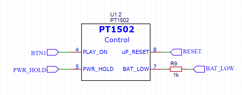
Also, the microcircuit can start the device by pressing a button (BTN1), as well as by a signal from the microcontroller (PWR_HOLD) to shut down and turn off the power. Well, in order to signal the processor that the battery is running out, the BAT_LOW signal is provided.
And this is the main power source.

The output voltage is set by the voltage at the BUCKFB pin and is set to 2V with battery power. But with two-volt power, one problem was discovered - USB will not work. Those.The battery will be charged, and the data will not be transferred - the microcontroller simply will not be able to output signals to the USB bus of sufficient amplitude. Datashit recommends a voltage of at least 2.7V, better than 3.3V.
In order not to fence another power source and think about how to switch between them, I decided to simply adjust the ratio of the divider R1 / R4 + R7. With this switch on, the impulse operates continuously. As soon as the device is plugged into USB, the transistor opens and shuns the R7. The ratio of the setting resistors changes and we get 3.16V at the output (it will be possible to play with the nominal values and finish it to 3.3V).
In the PT1502 chip, there are also 2 linear regulators.

I will have either little consuming components (INA219) or short-lived ones (bluetooth) connected to these regulators, so the efficiency of these sources will not be a problem. The LDO2 supply voltage can be configured using the LDO2_SETx signals.
Since I still have open-ended questions on power supply voltages, I decided to separate the jumpers to select the LDO2_SETx mode. Also, to be able to measure the actual consumption of the corresponding tire, I will also scout the jumpers JP1 / JP2 / JP3 per comb.
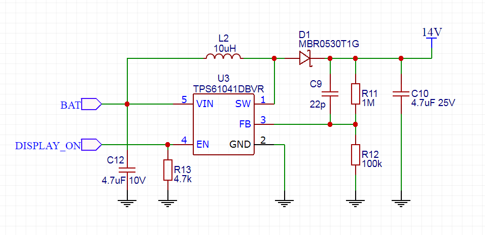
Finishing the topic of power supplies you need to mention the power of the display. Just above, I wrote that in the name of compactness, I had to abandon the purchased display module and pick up the display with strapping to my board. This display requires a special up-converter for 7-16V. Conveniently, this source can be turned on and off using the EN signal. The circuit itself is copied from the datasheet of the elevator, exactly the same used in display modules with Ali.
Now a little about the power of the microcontroller. The microcircuit is large and has 6 power lines - 4 for the digital part, 1 analog power supply and one for the clock. According to the datasheet on STM32F103 on all power lines (maybe, except for the clock), there should be a 100nF capacitor, and one more common at 4.7µF.
But in the datasheet on the STM32F4 it is said that although microcontrollers are practically compatible with the conclusions, the power circuits of them are somewhat different. So the two terminals should have 2.2 mkF capacitors between the output and the ground (and not between the ground and the power, as in F1). Therefore, it was necessary to take into account both options and for a specific microcontroller to solder only part of the capacitors.

Continuing the theme of nutrition, you need to figure out how to measure it. You can rely on the signal BAT_LOW and ask the user to quickly round out if the battery is low. But this is exactly what I did not like in the original Holux M-241, because this signal appeared too late and it was easy to miss it. I need some more informative indicator of battery charge.

Just in case, I put the most common divider to measure the voltage of the battery. But in the case of lithium batteries, this is only an informative indicator and it is not worth relying on it. For more honest testimony on the battery on the Internet offer to use the “pendant”.

This little microcircuit counts the amount of energy that has passed through to or from the battery. Measurements are made on the shunt R10. Chip readings can be read through I2C. The microcircuit is able to measure the voltage on the battery, the current passing through the resistor, and also to multiply one another. Unfortunately, it does not know how to accumulate the value of watches running past * Hours, so you will have to do a constant survey.
We turn to the digital part. The heart of the whole system is the STM32F103RB microcontroller.
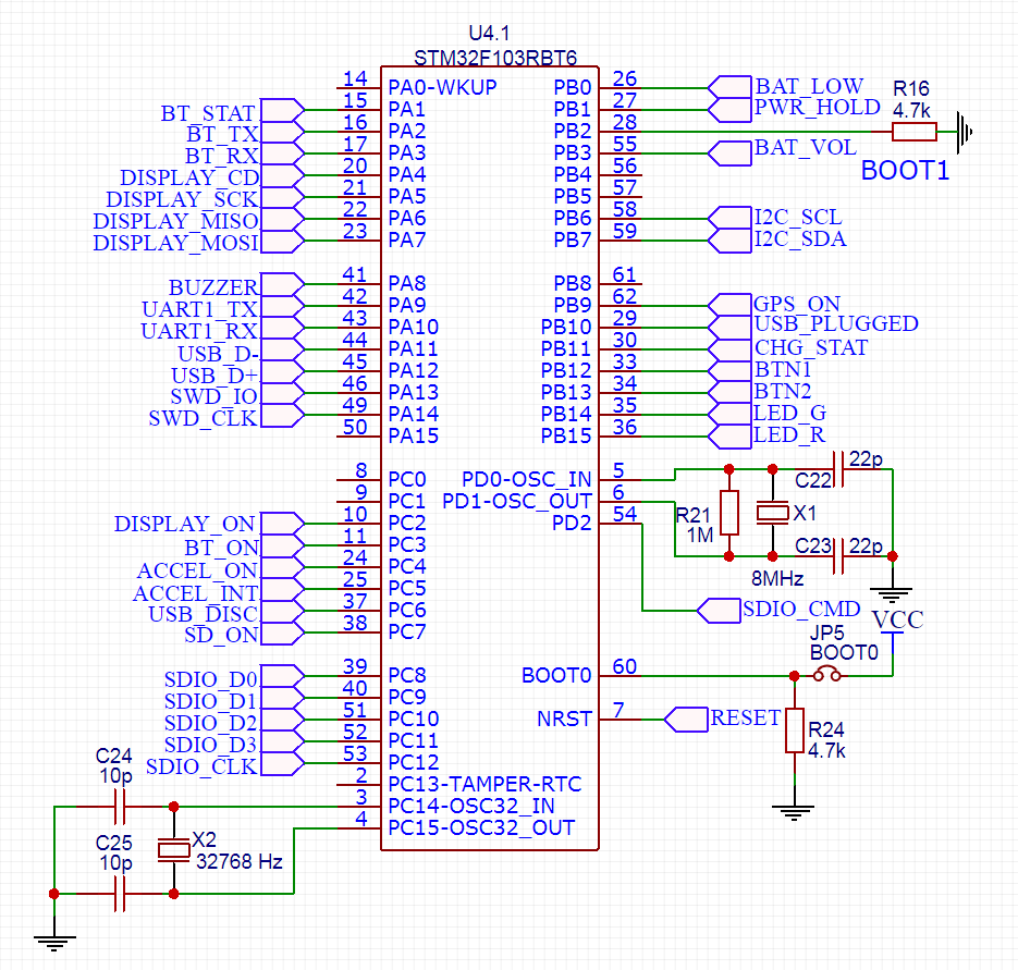
The binding in the form of two quartz is taken from other schemes found on the Internet (rechecked in datasheet). I do not need to load from RAM, but because the signal BOOT1 pulled to the ground. BOOT0 can be selected with a jumper for loading from the main flash memory or the built-in UART bootloader (for example, for the initial firmware of the device)
Next LED.

Since the main supply voltage will vary from 2 to 3.3V, it is not necessary to connect the LEDs to it - the brightness and current consumption will vary greatly. Therefore, my LEDs will be connected to the 2.7V bus, the current-limiting resistors are calculated accordingly. Since the microcontroller will not be able to issue more than 2V on its leg when powered by battery, the push-pull GPIO mode cannot be used. Only open-drain.
About the reset button to tell nothing special.

Since on the I2C bus there will be a three-volt device (INA219), then you also need to do suspenders for three volts

SWD connector is also standard. A diode is needed to switch power between the battery and external power from the programmer.

Anticipating exclamations that do not do so and that such a connection does not actually turn off the battery. Yes, do not turn off, but the diode is not here for this. This thing is needed to be able to power the device from the programmer if the battery is not connected. And if it is connected, then let it work from it. Well, if the battery is connected, then you need to protect the programmer from 4.2V on the battery.
But the buttons should stop in more detail.

The fact is that the first button will not only be a button, but will also work as a device switch - the signal BTN1 is connected to the chip of the power controller PT1502. When the device is powered off, the microcontroller and other consumers are not supplied. That is why the button is not connected to the power supply (VCC) but to the battery (BAT). By pressing this button, the PT1502 will turn on all power sources and start the microcontroller. After that, the button can work as a normal button. In order for the microcontroller not to burn with the high voltage of the battery, I built a small voltage divider that will drive the BTN1 signal into the required frames (however, it is possible without it - the microcontroller has 5V tolerant inputs)
The second button is unremarkable. Inside the processor, a pull up to the ground will be turned on, and the button will feed the unit to the line ...
Smoothly go to the heavy periphery. USB

The USB connector will stick out of the device, and static electricity can walk there. It turns out there are special chips (such as STF202-22), which protect microcontrollers from external influence.
But there is another interesting. A 1.5k resistor is hidden inside the STF202 chip, which is connected between the VBUS foot and the D + line. This resistor is required by the USB specification - the host will know from it that something has been plugged into it. In many circuits, this resistor is always connected between the power supply and the D + line. As soon as the host sees such a resistor on the D + line, it immediately starts communicating with the device. This is not always appropriate, since Some devices may not be immediately ready for communication.
This is just my case. For this there is a simple trick (peeped over here ). You can turn this resistor on and off with a transistor: we want communication — we turn on the resistor, we just want to be powered from USB — we turn it off. When you plug your cell phone into USB, he usually asks “what shall we do? Data to merge or only to be charged? ”- in terms of electronics, this is precisely the point of connecting a pull-up resistor.
But how do you know if the device is plugged into USB? For this, I provided a USB_PLUGGED signal, which is removed from the simplest divider.
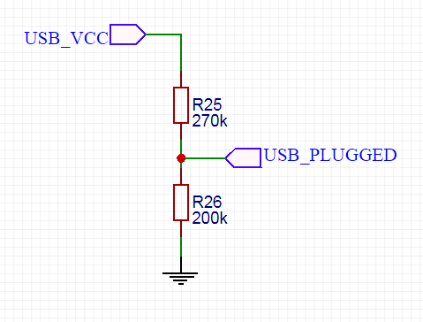
5V from USB could be sent directly to the leg of the microcontroller - they are still tolerant to 5V. But let it be through the divider.
Now accelerometer

The circuit is taken from datasheet. The module is connected via I2C, but to signal the microcontroller that there is news, the interrupt line is also used. Also, since the three-volt INA219 still hangs on the same I2C bus, to match the levels, the communication feet of the accelerometer are also powered from the 3V bus.
I already mentioned that I would like to save electricity and disconnect unused appliances. So the power of the accelerometer is switched on by the transistor.
By the way, I really liked the so-called. digital transistors - a transistor complete with two resistors. This saves a bit of board space. The only pity is that with a two-volt power supply I could not pick up a digital transistor with at least some decent current - 20-30 mA maximum. So the more voracious consumers had to connect MOSFET'ami.
Go ahead, GPS

GPS is located on a separate board and is connected via cable. Since I have not yet decided on the GPS module, I have provided 2 different power supplies. In addition to the power transistor on the side of the processor board there is nothing more interesting.
I can only say a few words about UARTs. Initially, I planned to use all 3 - one for uploading firmware and debugging, the second for GPS and the third for Bluetooth. But it turned out that UART3 is on the same pins as I2C No. 2, which I originally planned to use for the display. I had to choose. As a result, I came to the conclusion that I can upload firmware and debug through the same UART that is reserved for GPS (of course, GPS will have to be disabled). Well, if you need to debug the GPS itself, then there is also a USB CDC (in which you can upload logs) and SWD. Later, I abandoned the idea of using I2C # 2, so the UART3 was released, but in the name of saving the battery, I decided to stop at two UARTs.
Bluetooth
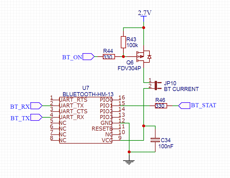
Bluetooth connects according to the scheme of datasheet. PIO1 output can operate in two modes. In the first, an LED is connected to it and the module is blinking with this LED. Different winking means different status. In another mode, this output works as digital — a unit when the connection is established, and 0 if not. Modes are switched by AT commands during module initialization.
SD card
Although the SD card connection scheme is standard, but for some reason it was very difficult for me. There are too many different connection options on the Internet and it’s hard to understand what’s right.
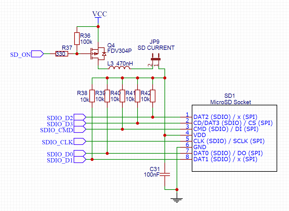
For the most part, I had questions in pass-through resistors. Occasionally there are circuits where 1k resistors are installed. Some circuits put resistors of 22 Ohms, apparently as a protection against static. Nevertheless, most of the circuits do not offer pass-through resistors, and I, perhaps, will go the same way. I also will not have statics. The flash drive will live inside the case.
The power transistor, as it seems to me, will also not be claimed, I think the card will always work - it's a logger. But since this is a test fee, then let it be. The same is true about the coil - apparently this inclusion was made paranoid in the original, or the card was used in an environment with poor power or noise. I think to solder the zero resistor there and try without a coil.
Display
I had the opportunity to connect one of the display modules with Ali via SPI and compare it with the connection via I2C. There were no particular difficulties, and the code only needed to be squandered. At the same time, the SPI speed is much higher than that of the I2C. Having added data from the datasheet on consumption (4 mA for SPI versus 10 mA for I2C), the need for pull-up resistors for I2C, I decided to connect the display via SPI.

Unfortunately, the BS0 signal is not displayed on the display loop, and therefore it is impossible to select the 3-Wire SPI mode, only 4-Wire SPI is possible. The difference is in the additional D / C line (data / command), which in the case of the 3-Wire mode are transmitted by the ninth bit of the SPI data. However, maybe 4-Wire mode is for the better, because SPI in STM32 can only transmit 8 bits.
The rest of the scheme corresponds to the datasheet.
And finally, the squeaker. Nothing special - just turn on through the transistor.

In case there is a vibration motor instead of a tweeter, I provided a protective diode. However, I heard the opinion that a protective diode also does not interfere with a beeper.
Above, I described my thoughts on the subject of the hull. In fact, I even tried to dilute the board for this case. Unfortunately, the fee was too close. I had to use double-sided mounting, to switch from components 1206 to 0805, but still the components on the board were very tight. Moreover, every change in the scheme was a pain, because I had to re-distribute almost half the fee.
So I fussed with it for several weeks, but the board won me over and the project I abandoned for almost a year. This article has become a kick. But indeed, this is only a prototype, with the first of several. Why bother with a super-compact board, where you can’t get a soldering iron or an oscilloscope, if you can debug everything on a large board?
Well, it is not necessary to do such a huge fee like an iPhone, but it’s quite possible to get into the promotional 100x100mm 2 layers of JLCPCB. You can hardly limit yourself. So the board has a huge 2.42 ”display, jumpers measuring consumption across all power lines, power capacitors where necessary and not needed, and in general a lot of parts that could not be installed. There is also a place left.
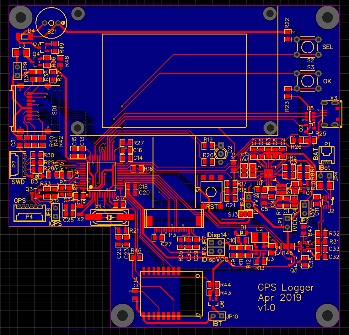
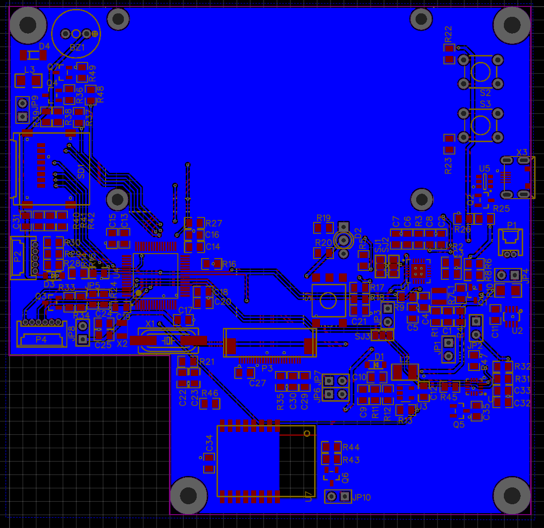
There is nothing to tell about the layout. I bred most of the signal and power lines on the upper layer, whereas the lower part was almost completely put under the ground. Unfortunately, the layout still turned out to be quite dense and some signal lines had to be dragged along the bottom layer through the half board. Because of this, the land in some places is “torn” on several weakly connected islands. I hope this will not be a problem.
I didn’t do the ground under the bluetooth antenna, but I still had to drag one of the signal lines through this zone. However, this is the BT_ON line, along which the signals often do not run (there it is either on or off), which means it should not influence the signal particularly strongly.
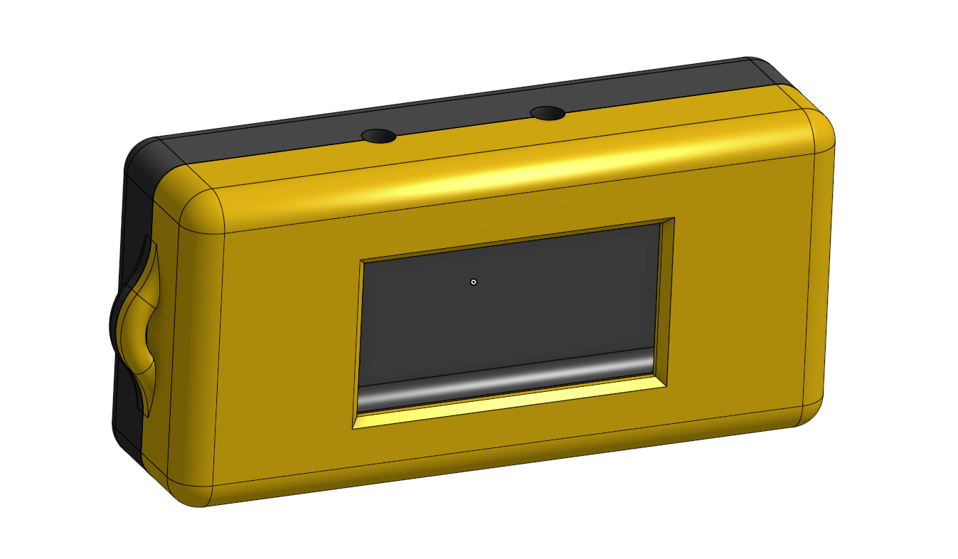
Summer was coming and I was planning to take a fee with me on vacation. So that the maids in hotels are not afraid of the bare debug board with a fan of wires, it would be nice to hide it in the case. I could not deny myself the pleasure and developed the case and the board at the same time. So there were mounting the board in the case, mounting the display holder.
The GPS module is a sandwich of several boards and an antenna 12mm thick. I decided not to cling to the board from above, but to place it on the same level. This reduced the thickness of the case, but one corner of the board bit off.
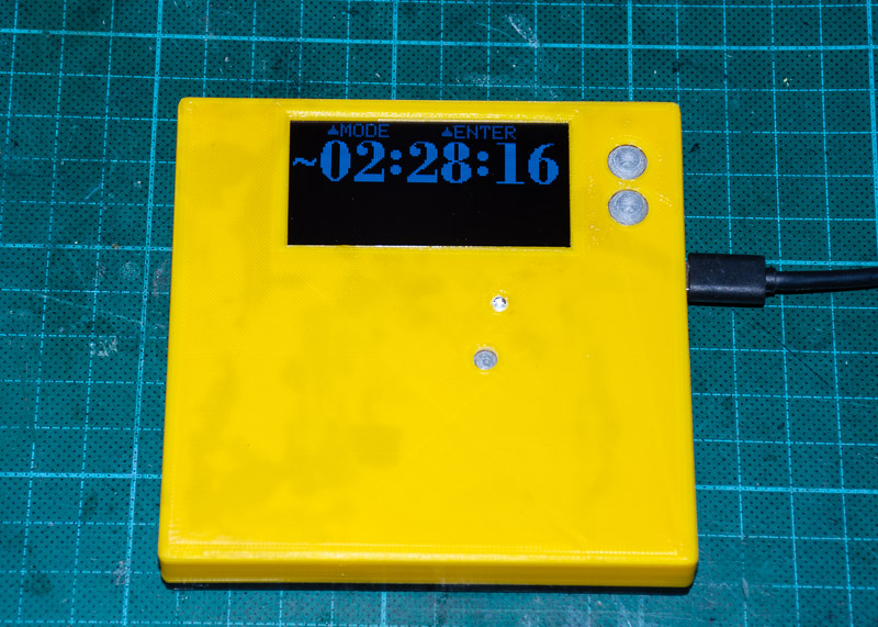
A couple of photos of the board and the final (at this stage of the project) device.
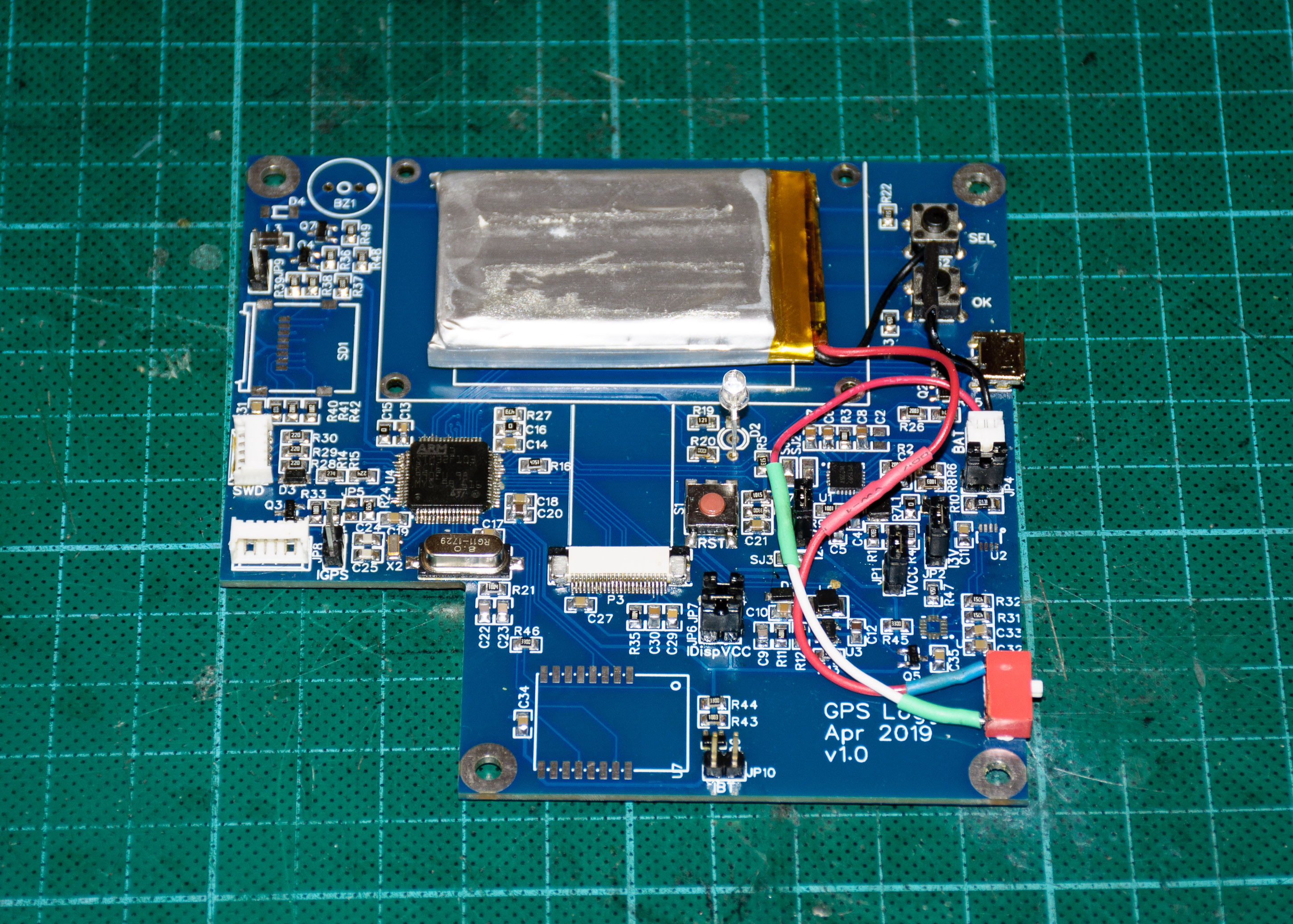


The battery is well placed under the display, but I had to make a small box in order to lift the display closer to the top cover.
A few words on the assembly board. I soldered everything for about 3 evenings, and about a week more in the evenings I spent on slow debugging and checking by the program part. To my surprise, there were no fundamental difficulties with setting up the board, and almost everything went right.
Loose 0805 was not much more difficult to solder than 1206, it is quite edible at home with a magnifying glass. You can even swing at 0603. But with the soldering of the microcontroller and the display connector (they have a 0.5mm pin pitch) I had to tinker. On people in YouTube, it somehow just looks - I spent it once with a soldering iron and that's it, but all my conclusions stuck instantly.
Not without minor problems. In some places there was not drunk, somewhere there was a “snot”. The footprint for the USB connector turned out to be wrong - he had a smaller lead pitch than necessary (so believe after that footprints from the Internet!). I had to bend the findings a bit so that they became on the tracks. The FPC display connector bought on Ali turned out to be with contacts from below, while I needed it with contacts from above (I had never been aware of such a difference before). I had to “blow off” the connector from the standard display board.
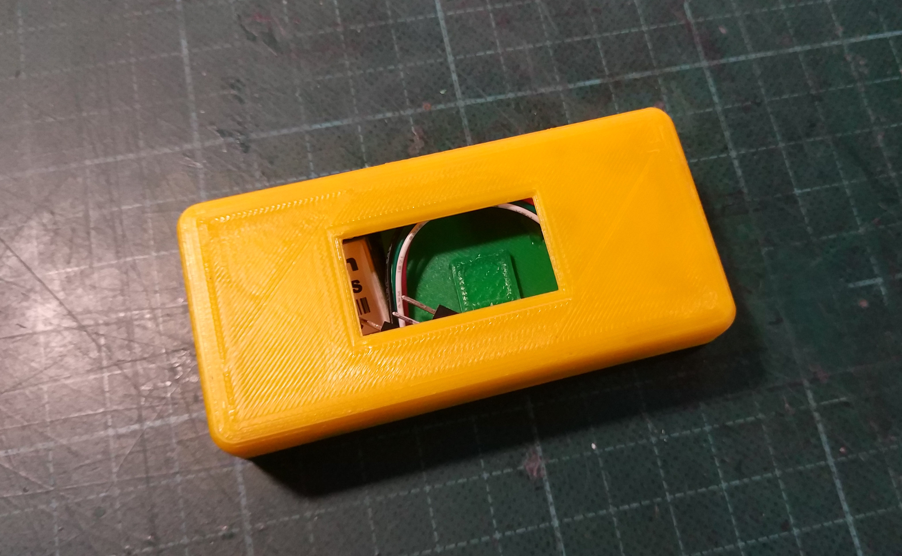
After stuffing the board into the case, it turned out that it was impossible to disconnect the battery simply by pulling out the connector, but I didn’t want to leave the unresolved board under voltage. I had to hit the switch.
When setting up the board, it turned out that there was no earth contact anywhere where the oscilloscope probe could be attached. I had to cling to the crocodile for the USB connector. It will be necessary to provide test sites in the next version of the board.
The circuitry also revealed problems. So a completely unexpected fact turned out that the PT1502 chip at the RESET pin generates a voltage of 3V (I was absolutely sure that there was something like an open collector). As a result, these 3B flowed to the power line, even though I planned to have only 2B there.
Here is a simplified diagram of what happened.

Thanks to the great reason and the guys from easyelectronics.com, this joint was decided to add one diode. After a small surgical procedure, this part worked as it should.
Next, the bluetooth module (powered by 2.5V) I inadvertently connected to the main power supply (2B), instead of the fixed 3V. Now my bluetooth can only work when USB is connected, when the main power supply voltage rises to 3.3V.
In principle, it would be possible to wave the scalpel and solder the bluetooth to proper nutrition, but the UART2 to which the bluetooth is connected is not tolerant to 5B (he himself read it in the datasheet at the analysis stage, he himself noted this in the text above, and eventually forgot ). Therefore, connecting the bluetooth to the power supply is higher than the power of the microcontroller is fraught ... In the next version of the board, I will simply connect the bluetooth to some other UART.
The DC-DC converter with variable voltage also worked as planned - when powered from the battery, it produces 2V regularly, and when you plug in the USB it rises to 3.16V (you need to play with the nominal values and drag it to 3.3V). But then another flaw of the circuit came out: you also need to be able to raise the voltage when powered by the programmer. I think it is treated by adding another diode. I'll try to play a little later.
Finally, during the work on the board, I still didn’t understand how to properly power the SD card from undervoltage. A short googling led to nothing. Apparently, you need to dive into reading specifications of specifications (which, in addition, are partially closed). In the meantime, I short-circuited R7 and the board is now powered by fixed 3.16V (3.3V). I will leave it so far for the next couple of months while I work on the program part.
Speaking of software. Surprisingly (although it is quite expected), but in general, everything went without problems. Since I was switching between one series of microcontrollers (from F103CB to F103RC), there was no need to rework the software part. Only pin numbers corrected, but added the inclusion of transistors. Nevertheless, there were 2 nontrivial moments with which I had to tinker.
The first is battery power. I debugged the board when powered by USB and everything worked well overall. But the board did not want to switch on from the battery. Those. It can work (if you turn it on when USB is connected, and then pull out the cord), but it does not work on a cold one.
According to the design of the PT1502 chip, the board should start like this. The user presses the BTN1 button and after a third of a second the chip turns on all power supplies. When everything is good with power, the PT1502 “releases” the RESET signal, thus starting the microcontroller. The processor, in turn, sets the PWR_HOLD signal to one, signaling that it has started. After that, PT1502 regularly supplies electricity to the circuit until the microcontroller lowers the PWR_HOLD signal to zero.
But it is in theory. In fact, as soon as the processor set the PWR_HOLD signal, the board was instantly turned off.I shoveled the entire power supply circuit, watched the oscillograms of the main signals, shuffled the code in the bootloader back and forth, but the problem could not be understood. I also sinned in the absence of a pull-down resistor on the PWR_HOLD line, which I forgot to install, but it is recommended by the datasheet (and most likely it is needed). But adding it to the canopy did not solve the problem. And only when I borrowed a four-channel oscilloscope everything became clear.
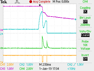
When the user presses the button (orange line), the PT1502 chip turns on the power (purple line). All this takes place long (300ms) before the events on this oscillogram. And then something interesting happens. PT1502 releases RESET (blue line), the processor starts up and for some reason lowers the button line to zero. Even though the microcontroller is still trying to raise the POWER_HOLD line (green line) - it's too late, PT1502 has already turned off all power supplies. Then there are a few more convulsions, but the scheme still quietly dies.
The question is where did the zero on the button come from? The whole thing is an inconspicuous error in the bootloader , because of which the output mode was set up on the BTN1's foot (perhaps miracles happened on other legs at that moment) and a low signal appeared there.
What else I had to face off with was an SD card. In the old microcontroller, the SDIO module simply did not exist, so this piece had to be studied from scratch. I spent almost the whole day trying to get a map, copying pieces of code from examples on the Internet and what CubeMX generated. Although the map was perfectly readable in the computer, I did not want to wind up in my scheme. I sinned on a bad solder, incorrectly chosen pull-up resistors, a clumsy circuit and a wrongly interpreted datasheet. But to my surprise, another card with the same code and on the same board started up without problems. It will be necessary to study this question in more detail.
There was another problem with the card. Having poked the oscilloscope in different lines, I saw activity only on the D0 line, while there was silence on D1-D3 - the card worked in one-bit mode. The HAL even showed up a HAL_SD_ConfigWideBusOperation () function that can enable 4-bit transfer mode. Unfortunately, when the card was transferred to 4-bit mode, the SDIO peripherals went to a deep RX FIFO Overrun and stopped working.
The problem turned out to be very interesting. It turned out that inside the HAL_SD_ReadBlocks () function there is a certain loop that polls the SDIO flags. As new data is received from the card, this code transfers the bytes from the internal FIFO buffer to the user memory. So the map transferred the bytes so fast that the code in HAL_SD_ReadBlocks () simply did not have time to shift the data. I had to temporarily lower the card clock frequency. Well, in the future I will use DMA and this problem should not arise in principle.
Those who are in this place expected to see the finished device I have to upset - only the test board is finished, and even then only the iron part. Now you need to breathe life into it, do software strapping, fine-tuning modes and consumption. Well, actually write the logging code - for the sake of what the whole project was started.
Nevertheless, for me personally, this stage is a very big and important achievement. Electronics is not my specialty and I am very glad that the device has started up at all. I managed to get quite strong in designing circuits, coordinating several devices, wiring a board, choosing components and much more than that.
I will tell you about the program part another time. As well as about the nuances of customization. The fact is that this entire filling must first be revived and tested. At the moment, it was possible to launch all the devices on the board (well, except for the tweeter), but only in the volume “it started and somehow responds”. No processing logic has been written yet.
Plans for the near future:
On this, let me take a bow. I would be grateful for constructive comments, ideas and advice on circuit design and PCB layout.
Sources:
Code
Code bootloader
Fee
Housing
In previous articles, I described the transition from arduino to STM32 , STMCube / HAL , talked a little about the build system , bootloader , built a composite USB device and pumped its speed . All this was done on a breadboard based on a Blue Pill STM32F103CB board and a hedgehog made from wires. It is time for the device to take shape, both electronic (circuit) and physical (body).
')
The issues that I had to solve at this stage are very interrelated. Choosing the components for the project you need to roughly represent in which body they can be shoved. Conversely, the body must be made for the components that are available and the board, which, again, must be done with an eye to the body. In general, a tangle of interrelated issues. You can, of course, take a bigger box and push anything there, but you want something compact and light.
Before I start right away, I want to note that this is not the final version of the device. Most likely, there will be errors in the scheme, something will not work as planned, they will indicate more correct solutions in the comments, some approaches will be rethought. I think that the second or even the third version of the device can not be avoided. Therefore, I will be glad to your constructive comments.
Under the cat mnogabukav, but it will be interesting.
What and why
The Holux M241 GPS logger is my faithful companion on all trips. He is with me for many thousands of kilometers. The track that the logger writes is primarily used for geotagging photos, but the route itself is also of interest. It's fun to find out how fast you went skiing, which route your plane flew, what sight just flashed past the bus window. Here I did a little review of this device.
Unfortunately, the capabilities of this device have long ceased to suit me: tired of fiddling with batteries, which always sit at the most inopportune moment. Also, a very small USB speed, a small amount of internal flash, an inconvenient mechanism for merging tracks, little information is available on the display, little accuracy, a very primitive odometer, no information about satellites, and a lot more on the little things.
Yes, it would be possible to look for what modern trackers offer - for sure there is already a device on sale that meets my requirements. But this is a hobby, I want to try myself to do something complicated, interesting, useful and necessary. Let it be even if I will be the only one to use it.
The goal of the project as a whole is to make a similar device in something, only stuffed with my Wishlist. In the first article of the cycle, I described in detail my device requirements. In short, I would like to do the following:
- recycle power system, convert to lithium battery
- put a more informative display
- more accurate GPS
- expand flash using sd card
- add compass and accelerometer
- I also want to rework the logging system to spit out the tracks in the format I need.
In addition to technical requirements and there is also a non-technical hotelok (non-functional). So I would like to improve the creation of complex devices from scratch, to understand how various electronic components work, how to program them, how to make a motherboard and design a case.
Why do you need a separate device if all modern phones have GPS, a big screen and a lot of memory? Well, first of all, I'm not sure that a phone with GPS enabled in track recording mode can withstand the whole day. I would not really like to stay in an unfamiliar country without a phone. Also, I personally use a separate device simply more comfortable.
Perhaps over time, the concept of the device will change. So, for example, now the idea of abandoning the screen and connecting to the phone via bluetooth is becoming more and more logical, and doing all the tricky logic already in the phone. This idea is very sensible and tempting. But at this stage, I would still like to have a display - I always have time to give it up.
For the first year and a half, I developed a device on various debugging boards (first arduino nano, then STM32F103 blue pill, then STM32F407VE). It was necessary to connect the periphery on postings and purchased modules. As a result, a hedgehog from the wires was obtained on the table, which could not be tested on the GPS reception; it was impossible to even move the wires without breaking the connection somewhere. And then happy debugging.
Every time I sat down to write useful functionality, I rested on the fact that some other part of the system stopped working normally and I had to spend hours debugging something completely unrelated. For example, the most important component of the system, the GPS receiver, turned out to be the least developed, since I had to go headlong into debugging USB, SD cards, setting up libraries and such.
Finally I got tired of it and I decided to make my debug board - this will be the topic of today's article. The goals that I set myself in this part of the project were:
- Make a debugging board that will not have problems with non-contact components
- Decide on basic technical and schematic solutions.
- Approximately decide on the components that I will use next
- Approximately decide on the layout and body
- The scheme should be general enough so that you can experiment with different components and their modes.
And although the ultimate goal is a compact battery device, today I will not do such things as
- fine tuning of power modes
- consumption setting
- sleep modes
I will deal with the consumption setting when the board and the main code are ready. By the way, about the code today, too, will not, but I will definitely return to this issue as there will be quite interesting material.
Components
Let's start with the components and peripherals. On the way, let us estimate the number of microcontroller legs that will be needed to connect this zoo, as well as the power options. Because This is a hobby project, that I chose the components from the fact that I really bought in the shops / ebay / ali, as well as the fact that you can solder at home (well, and also from what was already in personal stocks). Perhaps some specific chips could solve the problem better, but the issue of accessibility and price is important to me.
- The main component of the GPS logger, of course, will be a GPS receiver . In my case, this is a pretty tricked Beitian BN-880 based on the UBlox M8N chip. The module also has a compass on the HMC5883L chip.
Connection: 2 UART pins for GPS and 2 I2C pins for compass
Power supply: from 2.7V
Consumption: 50mA- Also ordered the module Beitial BN-220 . It does not have a compass, but the antenna is more compact (20x20mm vs. 30x30). The truth is still unclear how this will affect the quality of the reception. Need to test. But, judging by the datasheet, this module can work from 1.4V, which should have a positive impact on the operation time of the device.
- Here, in fact, everything is somehow dull. It seems that the BN-880 is based on the UBlox M8N, while the BN-220 is based on the U-blox M8030-KT. But in some sources it skips that it seems to be the same thing. More precisely, the M8N is a module, and the M8030-KT is a chipset inside. In this confusion, I am worried about the issue of power supply - the M8N is declared from 2.7V, while the M8030-KT is from 1.4V.
- Alternatively, I also have a SIM868 module lying around . in which on board, in addition to GPS, there is also a GSM / GPRS module and Bluetooth. So far, it is frightening with its cleverness and complexity of connection. You will need to play first with the debug board.
- The main difference between the device and “just a black box” is the presence of a display . In the first prototypes I connected the display via I2C, but the bus load was about 25%. But the matter is not even a percentage, but the fact that the screen buffer transfer takes about 25 ms, during which you cannot communicate with other devices on the bus. This can be a problem, so you need to either take out the display on a separate I2C bus, or consider connecting to SPI
Connection: 2 I2C wires or 3 SPI wires (display is write-only, so the MISO line is not used, but a separate Data / Command signal is used)
Power: from 3V
Consumption: 25mA - To control the device, I will use 2 buttons that take up 2 legs of the processor, respectively
- In the original device (Holux M241, from which I originally copied functionality) it was impossible to watch the track at an arbitrary point in time. It was necessary to connect the device to a computer and merge the data with a special program. As it seems to me, the opportunity to watch the track on a mobile phone or tablet at any time will be very much in demand. For this, I purchased a Bluetooth module HM-13 . This module is chosen because it can do SPP in addition to BLE.
Connection: 2 UART wires, 1 status wire (connected / not connected)
Power supply: 2.5V - 3.9V
Consumption: 50mA (although there is a 13mA figure next to it in the datasheet. Perhaps this is the peak and average value) - As I was told, it makes no sense to keep the receiver on, if you just sat down to rest or went to dinner at a cafe. Therefore, I decided to add the accelerometer MMA8452 and determine from it whether the device is at rest or we are moving somewhere.
Connection: 2 I2C wires, 1 interrupt wire
Power supply from 2V to 3.6V with some kind of microscopic consumption - GPS track will be recorded on the SD card . I have already tried using the card in SPI mode and this, to put it mildly, is slow. Especially on record. The correct mode for the SD card is SDIO
Connection: 6 wires
Power supply: from 1.8V
Consumption is unknown, but I think no more than 20mA - To save electricity, it makes sense to turn off the power of those devices that are not currently in use. So next to each consumer I will put on the transistor , which I will manage a separate signal of the microcontroller
Connection: 5 signals, one foot per consumer (GPS, Bluetooth, accelerometer, SD card, display) - Two-color LED to display status (as without a blinking LED?). It would be possible to put a tricolor, but for now I see no need.
Connection: 2 pins
Consumption: 10mA - In addition to Bluetooth, a more classic track-merging mechanism will be implemented via USB . For this, 4 lines will be used - a differential pair for data, 1 pin for detecting that the device was plugged into USB, and one more pin for logical connection (I will tell you about these 2 pins below)
- Appetite comes with eating. Since I started shoving everything into my dream device, why not add a squeaker ? Well, or vibromotor . Not yet invented yuzkeys.
Connection: 1 wire - The device will still need to be powered. While the PT1502 chip is looking at me as a lithium battery charger and power controller . To communicate with the microcircuit, you will need to use 2 wires: one for power management, the other for a signal about a dead battery. For the sake of interest, it will be possible to measure the voltage of the battery with the help of another line.
- Of course, the charge of a lithium battery is incorrect to measure on the basis of voltage. Therefore, I added a special microcircuit power meter INA219
Power supply: 3-5V, recommended 3.3V
Connection: 2 wires I2C
As will be seen below, the supply voltage in 3V creates some discomfort in the connection. I would prefer the IC chip to be powered by 2.7V or lower. But sorting through several options based on the price / housing / availability, I did not find anything on 2.7V. I would be grateful for the hint. - It remains only to provide a debugging interface SWD (3 wires) and a debugging UART (2 more wires)
I was always interested in the question of why we need controllers with a large number of ports, and I myself easily counted 39 paws needed for my functionality. And that's not counting quartz, reset, and power. And there are ideas about what to do with a dozen more (for example, the display could be connected via a parallel interface of the Intel 8080 or Motorola 6800).
You can, of course, fasten the I2C port externders to reduce the number of feet used. But firstly, these are additional components on the board, secondly, the software part is very complicated, and thirdly, there is still little memory in small microcontrollers, and where there is enough memory, there are also enough ports. So I do not see the point of complicating everything - let it be 39 lines.
Nutrition
With the supply voltage is not so clear. You can probably power all devices from 3.3V and calm down on this. But we, all the same, are going to do a mobile device, which means we need to think about saving energy. So you need to try to choose a smaller supply voltage. Below, I will figure out what kind of savings you can try to achieve.
Here is the data for all devices on the plate - in this form it is more convenient to choose the power domain to which to connect this or that device.
| Device | Power range | Power Domain | communication |
| CPU | 2 - 3.6V | 2V | |
| Accelerometer | 2 - 3.6V | 2V | I2C |
| Sd card | 1.8V or 3.6V | 2V | Sdio |
| Display | 1.65 - 3.3V or 3 - 5V | 2V | I2C or SPI |
| GPS | 2.7 - 5.5V or from 1.4V | 2.7V | UART |
| Bluetooth | 2.5 - 3.9V | 2.7V | UART |
| Power Meter (INA219) | 3 - 5.5V | 3V | I2C |
| Buzzer | 3V - 5V | Vbat |
From the plate it is easy to see that some devices can operate on sufficiently low voltages (from 1.8V). Others can comfortably work from 2.7V. Finally, the remaining devices below 3V cannot work. A squeaker, for good, generally needs 5V, but for me it will be powered by the highest voltage - from the battery, no matter how much it is.
With the power of the display is not yet fully understood. In the description of display modules with ali, a range of 3 - 5V is indicated, whereas in the datasheet on the matrix controller SSD1309 a range of 1.65 - 3.3V is indicated. I assume that 3V is needed to shake the boost converter on the display module board, whereas logic is 1.65V. As will be seen from the reasoning about the layout, it makes sense to abandon the display module and connect the display directly, which will power the display from domain 2B.
I have about the same reasoning about GPS - different sources indicate different supply voltages. So far I have no idea which module I will use as a result, so let the receiver talk in the domain 2.7B.
With an SD card is not at all clear. The specification says dimly that, in general, the card should be powered from 3.3V, but modern cards are smart enough and can understand that they have been plugged into a low-voltage device and can switch to 1.8V. But the mechanism of food selection is not very clear. I will power the card from 2B and see what happens. It will not work - it will work from 3B.
So, 4 power buses emerge - 2V, 2.7V, 3V and a battery. I would like to put all the hungry and constantly working consumers (and this is the controller and GPS) onto the lowest volt bus, but at the moment I have not yet decided on the GPS module (and therefore its power supply - 2 or 2.7V), which means it will be necessary some kind of universal solution. I will try to dissolve the board so that it is easy to apply either one or the other.
Where do we get so many different voltages? Even in the early stages of the project, I looked at the PT1502 microcircuit even managed to try it in another project . In addition to charging for a lithium battery in this chip, there are already 3 power sources - one pulse and 2 linear lowers. True, on one of them the voltage is not regulated and amounts to 3V - I will try to power the INA219 from it. The remaining 2 power sources are not a problem, because there voltage can be chosen.
Estimate consumption is not very successful. The datasheets indicate peak consumption - this is enough to calculate the power of the key transistors, but not enough to estimate the required battery capacity. So while the battery will be selected on the basis of available space in the case, and there I’ll measure the actual consumption.
The question may arise, but how to co-ordinate devices with different operating voltages? Let's figure it out.
- All the communication legs of the microcontrollers are marked as Five Volt Tolerant (except for UART2 on the legs of PA2 / PA3), which means that if there appears 3.3V from the highest-voltage device, nothing bad will happen
- The accelerometer, although powered by 2V, can potentially be connected in parallel with high-voltage devices on the bus. This problem is easily solved - the MMA8452Q chip can be used to separately power the communication pins from the other power supply (via the “high-voltage” device itself on the bus)
- I will try to power the SD card from the same voltage as the microcontroller, which means that nothing needs to be coordinated.
- GPS and Bluetooth should easily eat the “low” voltage from the microcontroller. The same applies to other “high-voltage” devices.
Finally, a few words about why I am so struggling to lower the supply voltage. The chip in a pulsed DC-DC converter that can exchange volts for amps (if you do not take into account the loss of the converter itself, of course). To be more precise, exchange higher voltage with low current for low voltage and higher current. In this case, we are more interested in reverse reasoning - if we power the low-voltage load through DC-DC, then the consumed current of this entire structure together with the converter will be lower than the consumed current of the load itself. Well, since battery capacity is measured in mAh, a decrease in current consumption will lead to an increase in battery life.
Calculate?
One friend suggested that since the efficiency of the converter is usually about 90%, it is quite possible that the complexity of the circuit in the form of DC-DC does not pay for itself and you can get by with the usual KRENKA. Let's estimate. I spent a couple of sooo rough calculations to see if the DC-DC converter is really appropriate here.
Here is a plate with calculations . Let the 900 mAh battery linearly discharge from 4.1 to 3.5V (which is generally not true). The efficiency of the DC-DC converter, I put 90% (the average value of the datasheet). Discharge will be 100mA current. I wanted to compare the operating time of the device from a linear power supply with a pulse.
Obviously, the line source will discharge the 900mAh battery with 100mA current in 9 hours. But with a pulse source, the device will last much longer - 9.3 hours at a target voltage of 3.3V, 11.4 hours at 2.7V, and a full 15 hours at a voltage of 2V. Of course, the calculations are, well, sooooo rough, but even so it is clear that with a pulsed source, the long life of the battery increases significantly.
Microcontroller
I approached the question of choosing a microcontroller thoughtfully - I played for a long time with the configurator, weighing all the pros and cons of each of the options. I really liked the STM32 microcontrollers, so I don’t see any point in looking towards other controllers without much need. Moreover, the STM32 line has controllers for every taste and for any periphery. The experience gained in the previous stages of my project allows us to narrow down the choice of controller based on the list of peripherals, the software already written, and the features that I would like to realize in the future.
So, it’s absolutely obvious that 20kb of my memory of my STM32F103CB is definitely not enough - there are not enough decent-sized buffers for communication between an SD card and USB. I haven't even started implementing much of the conceived functionality yet, and more than 19k are already taken. But with the power for processing, as it turned out, it is not particularly necessary. If all communication with the periphery is pushed into the DMA, then the share of the central processor remains only a couple of percent.
Having estimated the list of what I need from the controller, I counted the following:
- > = 128kb flash (about 50k is currently occupied)
- > = 40 kb of memory (19k currently occupied)
- > = 40 feet GPIO (see the reasoning above)
- > = 40 MHz (I don’t need much, the main thing is to have less consumption)
- DMA (I really liked it)
- > = 2x I2C,> = 3x UART,> = 1 SPI
- SDIO (flash drive via SPI is very slow)
- Honest USB Full Speed, Better High Speed
- Availability (the ability to buy a couple of pieces for an adequate price)
- From the wishes of the still native support for parallel LCD interfaces (usually implemented as an external memory access module FSMC)
STMicroelectornics microcontrollers are just a dime a dozen for every taste, color and wallet. At first I tried to proceed from the series when choosing a controller. The L0 and F0 lines are too weak and little memory, S7 and H7, on the contrary, are too sophisticated, L4 does not have SDIO (UPD: SDIO is, they just did not mention it on the title page of the series). Among the rest of the series, you can choose something based on my needs, since I have no particularly specific requirements.
The STM32WB series impresses with the presence of Bluetooth, but the VFQFPN68 case somewhat cools the desire to use it in hobby projects. And I did not find such controllers in retail.
I aimed at the body of the LQFP64 - sufficient for the number of legs, but it is not very big and can be soldered at home. It's good that there is a CubeMX configurator in which you can choose what you need by filters.
I chose the STM32F103RB controller for three reasons. Firstly, I have already studied the F103 series well using the example of the Blue Pill board. In general, the STM32F103CB controller completely suited me, but the memory was not enough. Secondly, I already have a bootloader and low-level code for this controller, while others will have to be redone. And thirdly, about a year ago, I already bought 3pcs of STM32F103RB for joy. Then I did not do a detailed study of the available controllers, but simply picked up a thicker controller from the F103 line. Do not throw it away now :)
As I have already noted, I do not have particularly specific requirements for peripherals or performance. But if I put something into something, then I already have controllers from the F4 line (if I need something more powerful), or L152RD, if I need to solve something with consumption (UPD: I looked after L433RC). What is good, with the STM32 almost all pin-to-pin controllers are compatible, and F4 and L1 / L4 can be soldered practically without reworking the board. You can even several boards with different MK to collect and compare consumption.
A few words about the body and layout
Determined with the details. It's time to draw a diagram, then trace the board, and then try to fit it into the case. Or not?Frankly, at first I just went this way, but then I came to the conclusion that everything must be done in the reverse order. Well, or at least at the same time.
I would like to get a compact device. And for this you need to accurately understand the size of the available space, in turn, to understand where to place the board and its size, what size battery can fit, where to place the buttons, screen, USB connector and other external components, and also figure out how to fix the components and you can Is it convenient to lay wires between them? Starting to make a fee without an understanding of all these pieces is simply meaningless. So it turns out that you need to first do the body and layout, and then go to the scheme.
Also in the process of drawing the case, I had to revise the choice of components several times. So initially I thought of using a cheap 128x64 display with a size of 0.96 ” (the size of the work area was 21.7 x 11.2mm), but this display looked completely microscopic against the background of a much larger case. Then a 1.3 ”display was ordered (working area 29.4 x 14.7 mm), but it didn’t get much better. Then I got a 1.54 ”display (35 x 17.5 mm) - it looks more or less normal with it. At the moment this is the main working version.
By estimation, a 1.8 ”-2” display would look better, but these are already color and more resolution, and accordingly the screen buffer will be large enough for my controller (35kb instead of 1kb). Well, with the pushing of large displays into the case there can also be problems, because The landing attachments for such modules are substantially larger than the active area of the display.
While I was writing this article on Ali, monochrome 2.42 ”displays appeared with the same resolution (128x64) and the exact same strapping as the 1.54”. I ordered myself a sample of this - there is a chance to stick it in my case without a significant increase in the device.
Another important point at the stage of working on the case was the understanding that the purchased display module takes up too much space and significantly reduces the space for the main board. So I decided to abandon the finished display module, and instead put the display and its strapping on my board. The number of parts in the scheme has increased slightly, but the design as a whole has become much simpler and more compact.
I have similar thoughts on the GPS module. It is not that big, but no matter how you put it, it either interferes, or the antenna is closed with some kind of battery. It may be a good idea to place the module stuffing on your board, and place the antenna somewhere else.
Work on the case also allowed to determine the size and capacity of the battery. The 900mAh battery was found in the available volume - we will be guided by it. I would like my device to run on a 15-20 hour battery, which means that the consumption should be at the level of 45-60mA.
At the moment I can not call the work on the body finished. First, the question of choice for some components (display, GPS) is still open. Secondly, it is not clear whether my scheme will start in principle or whether it will be necessary to change something cardinally. Well, thirdly, the board turns out to be too compact - I'm not sure that I can dissolve it, solder it and debug it. Therefore, in this article, I will nevertheless focus on the issues of circuitry, I will move with simpler and more understandable steps, and I will tell you about the case next time. Here's a couple of renderings and photos for starters.
Scheme
Now you can do electronics. I will describe in detail enough circuit solutions. First of all, for the same beginners in electronics as me, and also as a synopsis to myself. Experienced electronics engineers can skim through the diagrams and rewind to the next section.
Let's start with food.
The device will be powered by a lithium battery, which means you need a charge controller. Also, some components have an upper limit on the voltage of about 3.6V, while the battery can easily be greater than 4V. So you need a step-down power source. As we already found out, we will need several different voltages.
I have already mentioned that I will use the PT1502 chip. It fits well, because implements a charge controller, 3 power sources, as well as a device wiring diagram with a button. There are several functional blocks in the microcircuit, which I have divided for clarity in the diagram. The scheme itself is a slightly reworked datasheet scheme. Here is the lithium battery charge controller.
Resistor R3 sets the charge current. By default, this corresponds to 470mA. Perhaps by the results of the tests, I will reduce the value of this resistor to 510 ohms, which will give a charge current of about 900mA (1C).
The controller can report the current charge mode with the foot CHG_STAT. Moreover, he can give signals as much as 3 — he charges, does not charge, and is already charged, but still connected to the outlet. In the first embodiment, the internal transistor presses the foot to the ground and this can be easily recognized by the controller. In the second variant, the transistor closes completely and the leg goes into a high-impedance state. With the help of power-ups, such a signal is also easy to read as a controller.
But with the third state is not so simple. There, the transistor is ajar and a current of 20 μA flows through it. In order to consider such a state, I was prompted to choose a suspender in such a way that about half of the nutrition was on my leg. Then it will be possible to detect such a state with the help of an ADC. Using Ohm's law we get R5 = 1V / 20µA = 50k.
As I said, the PT1502 chip is not just a charger, but also a clever controller of the entire power supply. The microcircuit monitors the voltages on the circuit and with the help of the RESET signal can control the main processor (they say it's too early for you to start, the power has not stabilized yet).
Also, the microcircuit can start the device by pressing a button (BTN1), as well as by a signal from the microcontroller (PWR_HOLD) to shut down and turn off the power. Well, in order to signal the processor that the battery is running out, the BAT_LOW signal is provided.
And this is the main power source.
The output voltage is set by the voltage at the BUCKFB pin and is set to 2V with battery power. But with two-volt power, one problem was discovered - USB will not work. Those.The battery will be charged, and the data will not be transferred - the microcontroller simply will not be able to output signals to the USB bus of sufficient amplitude. Datashit recommends a voltage of at least 2.7V, better than 3.3V.
In order not to fence another power source and think about how to switch between them, I decided to simply adjust the ratio of the divider R1 / R4 + R7. With this switch on, the impulse operates continuously. As soon as the device is plugged into USB, the transistor opens and shuns the R7. The ratio of the setting resistors changes and we get 3.16V at the output (it will be possible to play with the nominal values and finish it to 3.3V).
In the PT1502 chip, there are also 2 linear regulators.
I will have either little consuming components (INA219) or short-lived ones (bluetooth) connected to these regulators, so the efficiency of these sources will not be a problem. The LDO2 supply voltage can be configured using the LDO2_SETx signals.
Since I still have open-ended questions on power supply voltages, I decided to separate the jumpers to select the LDO2_SETx mode. Also, to be able to measure the actual consumption of the corresponding tire, I will also scout the jumpers JP1 / JP2 / JP3 per comb.
Finishing the topic of power supplies you need to mention the power of the display. Just above, I wrote that in the name of compactness, I had to abandon the purchased display module and pick up the display with strapping to my board. This display requires a special up-converter for 7-16V. Conveniently, this source can be turned on and off using the EN signal. The circuit itself is copied from the datasheet of the elevator, exactly the same used in display modules with Ali.
PT1505
PT1502 — PT1505. , . . PT1505 .
, .
, .
Now a little about the power of the microcontroller. The microcircuit is large and has 6 power lines - 4 for the digital part, 1 analog power supply and one for the clock. According to the datasheet on STM32F103 on all power lines (maybe, except for the clock), there should be a 100nF capacitor, and one more common at 4.7µF.
But in the datasheet on the STM32F4 it is said that although microcontrollers are practically compatible with the conclusions, the power circuits of them are somewhat different. So the two terminals should have 2.2 mkF capacitors between the output and the ground (and not between the ground and the power, as in F1). Therefore, it was necessary to take into account both options and for a specific microcontroller to solder only part of the capacitors.
Continuing the theme of nutrition, you need to figure out how to measure it. You can rely on the signal BAT_LOW and ask the user to quickly round out if the battery is low. But this is exactly what I did not like in the original Holux M-241, because this signal appeared too late and it was easy to miss it. I need some more informative indicator of battery charge.
Just in case, I put the most common divider to measure the voltage of the battery. But in the case of lithium batteries, this is only an informative indicator and it is not worth relying on it. For more honest testimony on the battery on the Internet offer to use the “pendant”.
This little microcircuit counts the amount of energy that has passed through to or from the battery. Measurements are made on the shunt R10. Chip readings can be read through I2C. The microcircuit is able to measure the voltage on the battery, the current passing through the resistor, and also to multiply one another. Unfortunately, it does not know how to accumulate the value of watches running past * Hours, so you will have to do a constant survey.
We turn to the digital part. The heart of the whole system is the STM32F103RB microcontroller.
The binding in the form of two quartz is taken from other schemes found on the Internet (rechecked in datasheet). I do not need to load from RAM, but because the signal BOOT1 pulled to the ground. BOOT0 can be selected with a jumper for loading from the main flash memory or the built-in UART bootloader (for example, for the initial firmware of the device)
Next LED.
Since the main supply voltage will vary from 2 to 3.3V, it is not necessary to connect the LEDs to it - the brightness and current consumption will vary greatly. Therefore, my LEDs will be connected to the 2.7V bus, the current-limiting resistors are calculated accordingly. Since the microcontroller will not be able to issue more than 2V on its leg when powered by battery, the push-pull GPIO mode cannot be used. Only open-drain.
About the reset button to tell nothing special.
Since on the I2C bus there will be a three-volt device (INA219), then you also need to do suspenders for three volts
SWD connector is also standard. A diode is needed to switch power between the battery and external power from the programmer.
Anticipating exclamations that do not do so and that such a connection does not actually turn off the battery. Yes, do not turn off, but the diode is not here for this. This thing is needed to be able to power the device from the programmer if the battery is not connected. And if it is connected, then let it work from it. Well, if the battery is connected, then you need to protect the programmer from 4.2V on the battery.
But the buttons should stop in more detail.
The fact is that the first button will not only be a button, but will also work as a device switch - the signal BTN1 is connected to the chip of the power controller PT1502. When the device is powered off, the microcontroller and other consumers are not supplied. That is why the button is not connected to the power supply (VCC) but to the battery (BAT). By pressing this button, the PT1502 will turn on all power sources and start the microcontroller. After that, the button can work as a normal button. In order for the microcontroller not to burn with the high voltage of the battery, I built a small voltage divider that will drive the BTN1 signal into the required frames (however, it is possible without it - the microcontroller has 5V tolerant inputs)
The second button is unremarkable. Inside the processor, a pull up to the ground will be turned on, and the button will feed the unit to the line ...
Smoothly go to the heavy periphery. USB
The USB connector will stick out of the device, and static electricity can walk there. It turns out there are special chips (such as STF202-22), which protect microcontrollers from external influence.
But there is another interesting. A 1.5k resistor is hidden inside the STF202 chip, which is connected between the VBUS foot and the D + line. This resistor is required by the USB specification - the host will know from it that something has been plugged into it. In many circuits, this resistor is always connected between the power supply and the D + line. As soon as the host sees such a resistor on the D + line, it immediately starts communicating with the device. This is not always appropriate, since Some devices may not be immediately ready for communication.
This is just my case. For this there is a simple trick (peeped over here ). You can turn this resistor on and off with a transistor: we want communication — we turn on the resistor, we just want to be powered from USB — we turn it off. When you plug your cell phone into USB, he usually asks “what shall we do? Data to merge or only to be charged? ”- in terms of electronics, this is precisely the point of connecting a pull-up resistor.
But how do you know if the device is plugged into USB? For this, I provided a USB_PLUGGED signal, which is removed from the simplest divider.
5V from USB could be sent directly to the leg of the microcontroller - they are still tolerant to 5V. But let it be through the divider.
Now accelerometer
The circuit is taken from datasheet. The module is connected via I2C, but to signal the microcontroller that there is news, the interrupt line is also used. Also, since the three-volt INA219 still hangs on the same I2C bus, to match the levels, the communication feet of the accelerometer are also powered from the 3V bus.
I already mentioned that I would like to save electricity and disconnect unused appliances. So the power of the accelerometer is switched on by the transistor.
By the way, I really liked the so-called. digital transistors - a transistor complete with two resistors. This saves a bit of board space. The only pity is that with a two-volt power supply I could not pick up a digital transistor with at least some decent current - 20-30 mA maximum. So the more voracious consumers had to connect MOSFET'ami.
Go ahead, GPS
GPS is located on a separate board and is connected via cable. Since I have not yet decided on the GPS module, I have provided 2 different power supplies. In addition to the power transistor on the side of the processor board there is nothing more interesting.
I can only say a few words about UARTs. Initially, I planned to use all 3 - one for uploading firmware and debugging, the second for GPS and the third for Bluetooth. But it turned out that UART3 is on the same pins as I2C No. 2, which I originally planned to use for the display. I had to choose. As a result, I came to the conclusion that I can upload firmware and debug through the same UART that is reserved for GPS (of course, GPS will have to be disabled). Well, if you need to debug the GPS itself, then there is also a USB CDC (in which you can upload logs) and SWD. Later, I abandoned the idea of using I2C # 2, so the UART3 was released, but in the name of saving the battery, I decided to stop at two UARTs.
Bluetooth
Bluetooth connects according to the scheme of datasheet. PIO1 output can operate in two modes. In the first, an LED is connected to it and the module is blinking with this LED. Different winking means different status. In another mode, this output works as digital — a unit when the connection is established, and 0 if not. Modes are switched by AT commands during module initialization.
SD card
Although the SD card connection scheme is standard, but for some reason it was very difficult for me. There are too many different connection options on the Internet and it’s hard to understand what’s right.
For the most part, I had questions in pass-through resistors. Occasionally there are circuits where 1k resistors are installed. Some circuits put resistors of 22 Ohms, apparently as a protection against static. Nevertheless, most of the circuits do not offer pass-through resistors, and I, perhaps, will go the same way. I also will not have statics. The flash drive will live inside the case.
The power transistor, as it seems to me, will also not be claimed, I think the card will always work - it's a logger. But since this is a test fee, then let it be. The same is true about the coil - apparently this inclusion was made paranoid in the original, or the card was used in an environment with poor power or noise. I think to solder the zero resistor there and try without a coil.
Display
I had the opportunity to connect one of the display modules with Ali via SPI and compare it with the connection via I2C. There were no particular difficulties, and the code only needed to be squandered. At the same time, the SPI speed is much higher than that of the I2C. Having added data from the datasheet on consumption (4 mA for SPI versus 10 mA for I2C), the need for pull-up resistors for I2C, I decided to connect the display via SPI.
Unfortunately, the BS0 signal is not displayed on the display loop, and therefore it is impossible to select the 3-Wire SPI mode, only 4-Wire SPI is possible. The difference is in the additional D / C line (data / command), which in the case of the 3-Wire mode are transmitted by the ninth bit of the SPI data. However, maybe 4-Wire mode is for the better, because SPI in STM32 can only transmit 8 bits.
The rest of the scheme corresponds to the datasheet.
And finally, the squeaker. Nothing special - just turn on through the transistor.
In case there is a vibration motor instead of a tweeter, I provided a protective diode. However, I heard the opinion that a protective diode also does not interfere with a beeper.
In the gland
Above, I described my thoughts on the subject of the hull. In fact, I even tried to dilute the board for this case. Unfortunately, the fee was too close. I had to use double-sided mounting, to switch from components 1206 to 0805, but still the components on the board were very tight. Moreover, every change in the scheme was a pain, because I had to re-distribute almost half the fee.
So I fussed with it for several weeks, but the board won me over and the project I abandoned for almost a year. This article has become a kick. But indeed, this is only a prototype, with the first of several. Why bother with a super-compact board, where you can’t get a soldering iron or an oscilloscope, if you can debug everything on a large board?
Well, it is not necessary to do such a huge fee like an iPhone, but it’s quite possible to get into the promotional 100x100mm 2 layers of JLCPCB. You can hardly limit yourself. So the board has a huge 2.42 ”display, jumpers measuring consumption across all power lines, power capacitors where necessary and not needed, and in general a lot of parts that could not be installed. There is also a place left.
It's in Photo View

There is nothing to tell about the layout. I bred most of the signal and power lines on the upper layer, whereas the lower part was almost completely put under the ground. Unfortunately, the layout still turned out to be quite dense and some signal lines had to be dragged along the bottom layer through the half board. Because of this, the land in some places is “torn” on several weakly connected islands. I hope this will not be a problem.
I didn’t do the ground under the bluetooth antenna, but I still had to drag one of the signal lines through this zone. However, this is the BT_ON line, along which the signals often do not run (there it is either on or off), which means it should not influence the signal particularly strongly.
Summer was coming and I was planning to take a fee with me on vacation. So that the maids in hotels are not afraid of the bare debug board with a fan of wires, it would be nice to hide it in the case. I could not deny myself the pleasure and developed the case and the board at the same time. So there were mounting the board in the case, mounting the display holder.
The GPS module is a sandwich of several boards and an antenna 12mm thick. I decided not to cling to the board from above, but to place it on the same level. This reduced the thickness of the case, but one corner of the board bit off.
A couple of photos of the board and the final (at this stage of the project) device.
The battery is well placed under the display, but I had to make a small box in order to lift the display closer to the top cover.
A few words on the assembly board. I soldered everything for about 3 evenings, and about a week more in the evenings I spent on slow debugging and checking by the program part. To my surprise, there were no fundamental difficulties with setting up the board, and almost everything went right.
Loose 0805 was not much more difficult to solder than 1206, it is quite edible at home with a magnifying glass. You can even swing at 0603. But with the soldering of the microcontroller and the display connector (they have a 0.5mm pin pitch) I had to tinker. On people in YouTube, it somehow just looks - I spent it once with a soldering iron and that's it, but all my conclusions stuck instantly.
Not without minor problems. In some places there was not drunk, somewhere there was a “snot”. The footprint for the USB connector turned out to be wrong - he had a smaller lead pitch than necessary (so believe after that footprints from the Internet!). I had to bend the findings a bit so that they became on the tracks. The FPC display connector bought on Ali turned out to be with contacts from below, while I needed it with contacts from above (I had never been aware of such a difference before). I had to “blow off” the connector from the standard display board.
After stuffing the board into the case, it turned out that it was impossible to disconnect the battery simply by pulling out the connector, but I didn’t want to leave the unresolved board under voltage. I had to hit the switch.
When setting up the board, it turned out that there was no earth contact anywhere where the oscilloscope probe could be attached. I had to cling to the crocodile for the USB connector. It will be necessary to provide test sites in the next version of the board.
The circuitry also revealed problems. So a completely unexpected fact turned out that the PT1502 chip at the RESET pin generates a voltage of 3V (I was absolutely sure that there was something like an open collector). As a result, these 3B flowed to the power line, even though I planned to have only 2B there.
Here is a simplified diagram of what happened.
Thanks to the great reason and the guys from easyelectronics.com, this joint was decided to add one diode. After a small surgical procedure, this part worked as it should.
Next, the bluetooth module (powered by 2.5V) I inadvertently connected to the main power supply (2B), instead of the fixed 3V. Now my bluetooth can only work when USB is connected, when the main power supply voltage rises to 3.3V.
In principle, it would be possible to wave the scalpel and solder the bluetooth to proper nutrition, but the UART2 to which the bluetooth is connected is not tolerant to 5B (he himself read it in the datasheet at the analysis stage, he himself noted this in the text above, and eventually forgot ). Therefore, connecting the bluetooth to the power supply is higher than the power of the microcontroller is fraught ... In the next version of the board, I will simply connect the bluetooth to some other UART.
The DC-DC converter with variable voltage also worked as planned - when powered from the battery, it produces 2V regularly, and when you plug in the USB it rises to 3.16V (you need to play with the nominal values and drag it to 3.3V). But then another flaw of the circuit came out: you also need to be able to raise the voltage when powered by the programmer. I think it is treated by adding another diode. I'll try to play a little later.
Finally, during the work on the board, I still didn’t understand how to properly power the SD card from undervoltage. A short googling led to nothing. Apparently, you need to dive into reading specifications of specifications (which, in addition, are partially closed). In the meantime, I short-circuited R7 and the board is now powered by fixed 3.16V (3.3V). I will leave it so far for the next couple of months while I work on the program part.
Speaking of software. Surprisingly (although it is quite expected), but in general, everything went without problems. Since I was switching between one series of microcontrollers (from F103CB to F103RC), there was no need to rework the software part. Only pin numbers corrected, but added the inclusion of transistors. Nevertheless, there were 2 nontrivial moments with which I had to tinker.
The first is battery power. I debugged the board when powered by USB and everything worked well overall. But the board did not want to switch on from the battery. Those. It can work (if you turn it on when USB is connected, and then pull out the cord), but it does not work on a cold one.
According to the design of the PT1502 chip, the board should start like this. The user presses the BTN1 button and after a third of a second the chip turns on all power supplies. When everything is good with power, the PT1502 “releases” the RESET signal, thus starting the microcontroller. The processor, in turn, sets the PWR_HOLD signal to one, signaling that it has started. After that, PT1502 regularly supplies electricity to the circuit until the microcontroller lowers the PWR_HOLD signal to zero.
But it is in theory. In fact, as soon as the processor set the PWR_HOLD signal, the board was instantly turned off.I shoveled the entire power supply circuit, watched the oscillograms of the main signals, shuffled the code in the bootloader back and forth, but the problem could not be understood. I also sinned in the absence of a pull-down resistor on the PWR_HOLD line, which I forgot to install, but it is recommended by the datasheet (and most likely it is needed). But adding it to the canopy did not solve the problem. And only when I borrowed a four-channel oscilloscope everything became clear.
When the user presses the button (orange line), the PT1502 chip turns on the power (purple line). All this takes place long (300ms) before the events on this oscillogram. And then something interesting happens. PT1502 releases RESET (blue line), the processor starts up and for some reason lowers the button line to zero. Even though the microcontroller is still trying to raise the POWER_HOLD line (green line) - it's too late, PT1502 has already turned off all power supplies. Then there are a few more convulsions, but the scheme still quietly dies.
The question is where did the zero on the button come from? The whole thing is an inconspicuous error in the bootloader , because of which the output mode was set up on the BTN1's foot (perhaps miracles happened on other legs at that moment) and a low signal appeared there.
What else I had to face off with was an SD card. In the old microcontroller, the SDIO module simply did not exist, so this piece had to be studied from scratch. I spent almost the whole day trying to get a map, copying pieces of code from examples on the Internet and what CubeMX generated. Although the map was perfectly readable in the computer, I did not want to wind up in my scheme. I sinned on a bad solder, incorrectly chosen pull-up resistors, a clumsy circuit and a wrongly interpreted datasheet. But to my surprise, another card with the same code and on the same board started up without problems. It will be necessary to study this question in more detail.
There was another problem with the card. Having poked the oscilloscope in different lines, I saw activity only on the D0 line, while there was silence on D1-D3 - the card worked in one-bit mode. The HAL even showed up a HAL_SD_ConfigWideBusOperation () function that can enable 4-bit transfer mode. Unfortunately, when the card was transferred to 4-bit mode, the SDIO peripherals went to a deep RX FIFO Overrun and stopped working.
The problem turned out to be very interesting. It turned out that inside the HAL_SD_ReadBlocks () function there is a certain loop that polls the SDIO flags. As new data is received from the card, this code transfers the bytes from the internal FIFO buffer to the user memory. So the map transferred the bytes so fast that the code in HAL_SD_ReadBlocks () simply did not have time to shift the data. I had to temporarily lower the card clock frequency. Well, in the future I will use DMA and this problem should not arise in principle.
Conclusion and further steps
Those who are in this place expected to see the finished device I have to upset - only the test board is finished, and even then only the iron part. Now you need to breathe life into it, do software strapping, fine-tuning modes and consumption. Well, actually write the logging code - for the sake of what the whole project was started.
Nevertheless, for me personally, this stage is a very big and important achievement. Electronics is not my specialty and I am very glad that the device has started up at all. I managed to get quite strong in designing circuits, coordinating several devices, wiring a board, choosing components and much more than that.
I will tell you about the program part another time. As well as about the nuances of customization. The fact is that this entire filling must first be revived and tested. At the moment, it was possible to launch all the devices on the board (well, except for the tweeter), but only in the volume “it started and somehow responds”. No processing logic has been written yet.
Plans for the near future:
- Drive electronics in different modes, check that the circuit still works. Fix the jambs in the second version of the board
- Measure consumption of all peripherals and find ways to optimize consumption.
- Collect several board options on different microcontrollers (for example, on L152 or L433)
- Thoughtfully read the SD specification and figure out how to properly connect the card in the Low Voltage Signaling mode (1.8V)
- Try different GPS modules and, finally, decide on how I will go further
- Order a separate compass chip (for example HMC5883L or HSCDTD008A) and try to use them somehow
- To do internal code refactoring, upgrade all major libraries, starting with HAL
- Start, finally, write features. Actually implement what the device was intended for
On this, let me take a bow. I would be grateful for constructive comments, ideas and advice on circuit design and PCB layout.
Sources:
Code
Code bootloader
Fee
Housing
Source: https://habr.com/ru/post/454434/
All Articles