What's in a pixel for you my: the creation of nanopixels using plasmon meta-surfaces

Take a look at the screen. What do you see? A website page with text and pictures, right? But what if you dig deeper? All of these different in semantic load and presentation method elements consist of digital visual "atoms", called pixels. The more pixels - the better, with the exception of some indie games. Pixels, like any "atom" in the universe, has its own specific properties and limitations. At least it was before. Today we will get acquainted with the study, which describes the method of creating a new type of pixels, hundreds of times smaller and better than the current ones. How exactly did the scientists manage this, what amazing characteristics do the new pixels have and could these pixels help us to make out what is happening in the darkness of the third series of the eighth season of the Game of Thrones? We will look for answers in the report of the research group. Go.
The basis of the study
The word pixel we hear quite often and from a variety of sources. A new smartphone with a 20 megapixel camera (megapixels), a new pixel indie game, pixel art, a not-so-successful Pixel movie of 2015 with Tirion Lannister, i.e. with Peter Dinklage (sorry, PTSD after the Game of Thrones marathon), etc.
')
Scientifically speaking, a pixel is the smallest logical element of a two-dimensional image (voxels play this role in a three-dimensional image). If you compare any image on your screen with the sea, then the pixel is a drop of sea water, exaggeratedly speaking.
Pixels are round or rectangular (square) shape. Unlike spy movies and TV series about super-detectives, if you enlarge any digital image, then sooner or later it will turn into a bunch of squares of different colors, and not into a super clear image.

Poster series "Game of Thrones" with the King of the night.
The word “pixel” itself has a slightly astronomical origin. In 1965, Frederick Billingsley, from the Jet Propulsion Laboratory, first used this word to describe the graphic elements of video images from space probes of the Moon and Mars. At the same time, Mr. Billingsley was not a pioneer in the field of word formation, because before him this word was still used by Keith Macfarland in 1963. The English version of “ pixel ” can be divided into two components - “ pix ” ( picture - picture) and “ el ” ( element - element).
History is history, but we are not here for the sake of it, but for fresh discoveries.
The basis of this research is the meta-surfaces previously mentioned in previous articles.
Metamaterial * is a composite (of several components), whose properties depend not so much on the properties of its constituent elements, but on its overall structure (topology, architecture, etc.).Recently, scientists have been paying more and more attention to plasmonic * (not to be confused with plasma) meta-surfaces.
In turn, meta-surfaces are a two-dimensional type of metamaterials, which are characterized by low losses when working with light and are easy to manufacture.
Plasmon * is a quasi-particle corresponding to the quantization of plasma oscillations, which are collective oscillations of a free electron gas.However, there have always been difficulties in working with plasmon meta-surfaces, despite all the technical advantages.
In this study, scientists describe a method for creating a new type of scalable, electrically controlled meta-surfaces. In the process of creating a novelty, a bottom-up approach was used (the formation of nanoparticles from smaller elements, that is, from smaller to larger). And now more.
Sample preparation
Scientists remind us that plasmon resonances in combination with nanostructures of precious metals have become an excellent tool to improve certain optical phenomena and processes.
The use of plasmons in nanolithography to create displays is also very promising, since plasmon components have a wide color spectrum and a very small size, even smaller than ordinary pixels. But to this day, it was possible to implement exclusively static colors using a very complex process of adjusting and arranging scattering elements to overcome dependence on the polarization of light, viewing angle and illumination. In other words, it was possible before, but damn hard.
If we want to get active plasmon colors, scientists say, it is necessary to control the optical properties of the environment from the outside. For example, if you use plasmon meta-surfaces in conjunction with electrochromic materials (conductive polymers and materials with a phase transition), you can get "on / off" when the charge state of the electrochromic material changes. And this already doubles the refresh rate and optical contrast in comparison with systems where there are only electrochromic materials.
Considering that the size of plasmons regulates the color generation of RGB * pixels, scientists used electro / chemical means to enable plasmonic nanoparticles to function as small optical switches / pixels.
RGB * (red, green, blue) or GLC (red, green, blue) is an additive color model.For example, Au (gold) nanostructures, coated with Ag (silver), exhibit a wide color dynamics due to electrochemical control of Ag shell thickness or redox reactions. However, at the same time, such nanostructures are very short-lived (no more than 1 month), and their switching speed is very small (more than 0.5 s).
Such deficiencies are associated mainly with silver. When it is too often precipitated or it often goes through an oxidation / reduction process, the diffusion of ions occurs more slowly and leads to rapid morphological changes at the nanoscale. It turns out that the method is good and working, but not very durable.
Another way to achieve the desired is to apply a multilayer plasmon composite with a dielectric gasket (NPoM) inside.
NPoM - nanoparticle-on-mirror (nanoparticle-on-mirror).Another good thing is that such composites can be created without the use of problem lithography, but the accuracy will be down to the atomic level.

Image number 1
The main advantage of this structure is that nanoparticles severely limit the light inside their individual cells to the underlying mirror and, thus, create extremely localized optical resonators (image above). Thus, the nanoparticles become independent of each other and insensitive to the angle and polarization of the incident light.
Scientists note that this technology has not previously been used to create displays. And their main task is to implement the ability to produce NPoM on a large scale, while maintaining the independence of individual nanopixels.
In their work, scientists describe the creation of eNPoM - electrochromic nanoparticles-on-mirrors, formed from gold nanoparticles encapsulated in a conductive polymer shell of polyaniline.
The biggest achievements are the performance and energy efficiency of eNPoM. Switching the charge state of the shell allows you to quickly shift the color of the resonant scattering of eNPoM in the wavelength range> 100 nm. An active nanopixel in such a system requires only ~ 0.2 fJ (femtojoule, 1 fJ = 10 −15 J) energy for each wavelength shift by 1 nm.
ENPoM theory
Color dynamics based on local surface plasmon resonance ( LSPR ) works by changing the refractive index of the medium surrounding the plasmon nanomaterial, shifting the position of the LSPR peak. Appropriate color adjustment can be inferred from the sensitivity of the LSPR:
where λ is the resonator wavelength, x is the shape factor of the metal nanoparticle (if equal to 2, then it is a sphere), ℇ m is the dielectric constant of the metal nanoparticle and n is the refractive index of the medium surrounding the nanoparticle. In the best-case scenario, ∆n should be large, providing n ~ 1 to maintain the LSPR resonance in the middle of the visible region, and allowing ∆λ * to tune to the entire visible spectrum.
The use of plasmon nanoparticles is a logical solution in this situation, however there are a number of problems. Inorganic materials with a large ∆n form factor of> 2. Because of this, their LSPR resonances are in the near-infrared region (NIR) and are not suitable for the use of plasmon color. Sensitive polymers can be used in which n <1.7. But with such materials it is difficult to adjust and adjust the color.
It turns out that classical methods cannot be applied, more precisely it is possible, but the result will be weak. That is why scientists have used eNPoM ( 1a ), consisting of Au nanoparticles encapsulated in a polyaniline shell (hereinafter PANI). This NPoM topology manifests itself as a dimeric pair of plasmon particles that do not interact with each other, which causes an increase in the coupling of the optical field in the gap, known as the “hot spot” ( 1b ). This region leads to the formation of an additional bound resonance and a transverse mode of about 550 nm, supported only by Au nanoparticles alone.
Changing the surrounding optical medium allows you to adjust this resonance, and the transverse mode at this moment practically does not change. Change in the redox state of the ultra-small volume of the PANI shell surrounding each nanoparticle ( 3x10 -4 µm -3 ).
Having performed the finite-difference modeling in the time domain ( 1c ), the scientists suggested that the full redox effect of PANI in the eNPoM could lead to visible scattering wave shifts> 100 nm, i.e. 300% more than those supported exclusively by nanoparticles ( without the participation of the shell of polyaniline). In the reduced state of PANI 0, the coupled eNPoM resonance appears at c 0 = 675 nm, and when oxidized to PANI 2+ , a shift to blue color occurs at c 2+ = 575 nm.
Scattering at optimal eNPoM predicts a 100-nm color range with 43% adjustable contrast ( 1s ). Such observations suggest a real possibility to obtain custom / switchable colors with low optical losses and high spatial resolution, which was confirmed by experiments on devices with a single nanopixel ( 1d ).
Create eNPoM

Image number 2
The process of creating an eNPoM consists of two stages of the bottom-up method: coating the Au nanoparticles with a PANI coating in solution; low tide on a flat mirror Au.
Colloidal Au nanoparticles were encapsulated in a holistic thin PANI shell by chemical oxidative polymerization using a surfactant (inset in the upper right corner at 2b ).
Then, the obtained samples were built into electrochemical cells (cells) created in the laboratory, optimized for simultaneous tracking of optical and electrical dynamics.
The mirror from Au forms the working electrode, and the redox state of the PANI shells is controlled by changing the voltage from -0.2 to 0.6 V with a scanning speed of 50 mV / s. Cyclic voltammetry curves averaged over 90 cycles ( 2a ) show two sets of oxidized (top) and reduced peaks (bottom) of three different redox forms of PANI: PANI 0 is fully reduced; PANI 1+ is semi-oxidized and PANI 2+ is fully oxidized. Consequently, complete oxidation and reduction of eNPoM occurs only in the potential range ∆V <1 V. At the same time, the measurement of the “dark field” scattering spectrum of one eNPoM ( 2b and 1d ) occurs.
The application of a negative potential causes a decrease in the PANI shell (PANI 0 ), which leads to a scattering peak at c 0 = 642 nm. A reverse potential leads to a resonance shift up to c 2+ = 578 nm, while ∆λ * = 64 nm is consistent with the simulation carried out earlier ( 1c ).
Further observation of the dark-field scattering spectrum during cyclic voltammetry showed highly stable and reversible optical switching ( 2c ) with fully reproducible dynamics ( 2d ).
Even more important observation is the identity of all eNPoM from the standpoint of optical dynamics: if the conditions for all nanopixels are the same, then their optical dynamics will be the same, which is extremely important for large-scale homogeneous meta-surfaces.
Different gaps on eNPoM

Image number 3
After the preparatory work, the scientists decided to check how the structural parameters of the eNPoM affect color switching, in particular, how the “gaps” of the eNPoM, determined by the thickness of the shell on the surface of Au nanoparticles, affect this process. For this, several eNPoM test samples with different gaps were created, and the shell thickness was increased from 10 to 20 nm.
As a result, 4 types of eNPoM nanopixels were obtained: 11, 13, 18, and 20 nm ( 3a ). Scientists have evaluated their electrical ( 3b ) and optical dynamics ( 3c - 3f ).
Simulations and actual experiments with different nanopixels showed similar results - reversible blue shifts ( 3d ) and ~ 50% ( 3e ) intensity reduction during oxidation.
In theory, according to scientists, as the gaps decrease, the length of the resonant wave and the range of its spectral tuning should increase. In reality, everything turned out differently - the thinning of the PANI shell led to a smaller color range during the redox cycle. The researchers explain this with additional structural factors that were not taken into account in the modeling (in theory):
- imperfection of the spherical shape and size of Au nanoparticles;
- differences in the optical properties of PANI of different thickness;
- the heterogeneity of the PANI shell covering the nanoparticle;
- ~ 30% change in shell thickness during the redox process;
- the heterogeneity of the redox process of PANI shell molecules in the gap.
As a result, NPoM with a thicker shell (more than 15 nm) showed excellent color characteristics with high accuracy, consistent with mathematical modeling.
Redox Monitoring
The color change during a change in the redox state of a conducting polymer makes it possible to track the associated electron dynamics in the tiny channel under individual single nanoparticles in the NPoM geometry ( 4a ).
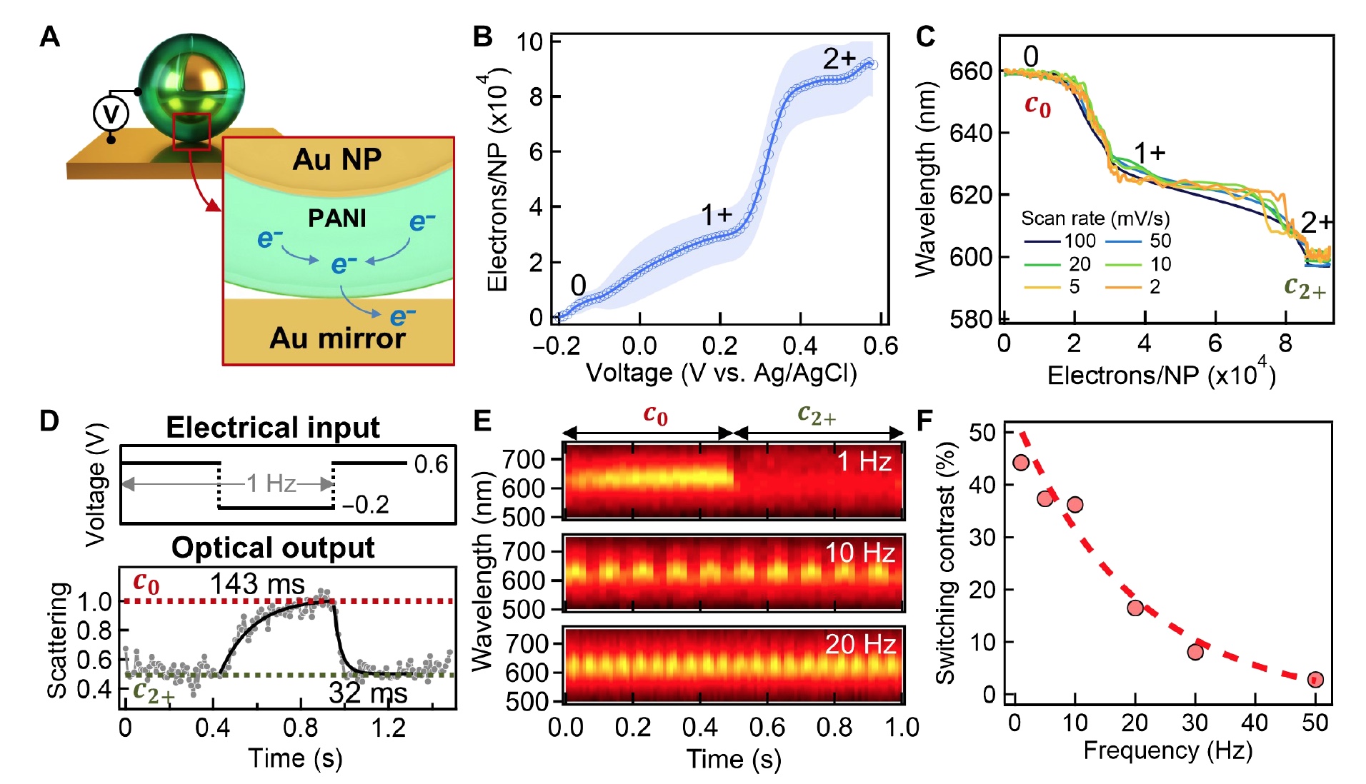
Image number 4
This allows you to understand how many electrons are transferred through the gap in the eNPoM and at what speed.
The transfer rate of electrons between the PANI and the mirror from Au is rather high due to the fact that this process takes place in nano-gaps with little mass transfer. This ensures that the redox system is electrochemically reversible. The peak current i P on the cyclic voltammetry curve in the oxidized (or reduced) state of the eNPoM is linearly proportional to the potential scanning speed n with a limited peak shift.
From this it follows that i P = vF 2 fA / RT with the participation of two electrons, where F is the Faraday constant (C / mol), R is the ideal gas constant (J / (mol K)), T is the system temperature (K ), A is the area of the working electrode (m 2 ), f is the surface area of the particles on the electrode (mol / m 2 ).
Given the linear relationship with n, f is constant and gives the number of PANI molecules undergoing electron transfer, which is given by the number of eNPoM on the electrode. This will allow you to calibrate the number of injected / extracted electrons from each NPoM ( 4b ). Thus, it is possible to see the dynamics of electrons in the gaps of individual NPoM, associated with three different oxidation-reduction states of PANI. Approximately 30,000 electrons in each nanoparticle are transferred. Measurements of optical dynamics showed two clear transitions that perfectly match the dynamics of electrons ( 4c ).
The main conclusion from the above observations is the energy efficiency of nanopixels - it takes ~ 80 and ~ 200 AJ (attojoule, 1 AJ = 10 −18 J) per 1 nm shift to switch color from c 0 to c 1+ and from c 1+ to c 2+ wavelength.
Next, the researchers analyzed the optical switching of single eNPoM with faster rectangular electrical modulation ( 4d above) to determine the temporal characteristic. In the case of applying a voltage jump from 0.6 to -0.2 V, causing rapid changes in the coupled mode from c 0 to c 2+ , a sharp redox transition of the polymer was observed ( 4d from the bottom).
The switching time was 32 ms (oxidation) and 143 ms (decrease) with a 47% change in intensity. Reversible color switching at the level of single nanoparticles is observed in response to rectangular potentials of increasing frequency up to 50 Hz ( 4e , 4f ).
Due to the stability of the charge states of PANI, the bistability (two equilibrium states) of eNPoM was observed. In addition, the resonance modes at c 2+ and c 0 persist for> 10 minutes. And this is one of the factors reducing energy consumption for a device based on this technology.
Scaling eNPoM meta-surfaces
Energy efficiency is, of course, good, but scalability is also needed. It is even better to combine these two indicators, avoiding lithography in production, as the researchers say. To achieve this, a new method of assembling nanoparticles by means of meniscus * targeting was applied.
Meniscus * is a concave-convex or convex-concave lens, bounded by two spherical surfaces.The volume fraction of particles in the solution used for coating determines the density of particles (filling fraction) on the mirror substrate (image No. 5). Surfaces consisting of randomly distributed eNPoM, with a filling percentage of 20%, are obtained using a 0.3% volume fraction of the original colloid.

Image number 5
A ~ 100 nm interval provides the minimum optical coupling of the near field between nanoparticles ( 5a ). Colors are controlled solely by the gaps under each eNPoM. The resulting increased eNPoM meta-surface also demonstrated excellent color switching with ∆λ * = 79 nm and 57% contrast switching across the entire surface ( 5b - 5e ). In other words, the meta-surface of an eNPoM exhibits the same properties and behavior as an individual eNPoM.
It is possible to improve the color range and dynamics in the meta-surface by mixing different nanoparticles or by using ultraviolet plasmon nanoparticles.

Image number 6
The graphs above show how good the characteristics of the developed system based on eNPoM nanopixels. The setting of the visible wavelength, ultra-small pixel size and switching speed meet modern requirements (green area at 5a ).
Scientists note that the developed meta-surface has been operating for 3 months (at the time of writing the report) at power densities below 300 mW / cm 2 and at a pixel density of 109 per square inch.
For a more detailed acquaintance with the nuances of the study I recommend to look into the report of the research group and additional materials to it.
Epilogue
The study reviewed today belongs to the category of improving existing technologies. However, at the same time, scientists used very radical, as they themselves call them, methods of nanotechnology to achieve the desired result. Light behaves very unusually at the nano-level, and an understanding of its properties and characteristics allows you to create new devices and improve existing ones.
Developed nanopixels can find their application in different areas - from displays the size of a house to camouflage materials. Scientists themselves are confident in this. They will continue to work on their invention, expanding its capabilities and improving its characteristics.
Friday off-top:
The confrontation of the avengers and Thanos ("War of Infinity") in the old school form.
The confrontation of the avengers and Thanos ("War of Infinity") in the old school form.
Off-top 2.0 (Valar Morgulis)
What would an old school fighting game look like with the characters from Game of Thrones.
Thank you for your attention, stay curious and have a great weekend, guys! :)
What would an old school fighting game look like with the characters from Game of Thrones.
Thank you for your attention, stay curious and have a great weekend, guys! :)
Thank you for staying with us. Do you like our articles? Want to see more interesting materials? Support us by placing an order or recommending to friends, 30% discount for Habr's users on a unique analogue of the entry-level servers that we invented for you: The whole truth about VPS (KVM) E5-2650 v4 (6 Cores) 10GB DDR4 240GB SSD 1Gbps from $ 20 or how to share the server? (Options are available with RAID1 and RAID10, up to 24 cores and up to 40GB DDR4).
VPS (KVM) E5-2650 v4 (6 Cores) 10GB DDR4 240GB SSD 1Gbps before summer for free if you pay for a period of six months, you can order here .
Dell R730xd 2 times cheaper? Only we have 2 x Intel TetraDeca-Core Xeon 2x E5-2697v3 2.6GHz 14C 64GB DDR4 4x960GB SSD 1Gbps 100 TV from $ 199 in the Netherlands! Dell R420 - 2x E5-2430 2.2Ghz 6C 128GB DDR3 2x960GB SSD 1Gbps 100TB - from $ 99! Read about How to build an infrastructure building. class c using servers Dell R730xd E5-2650 v4 worth 9000 euros for a penny?
Source: https://habr.com/ru/post/452086/
All Articles