Development of Full Self-Driving Computer
Translation of the first part of the Tesla Autonomy Investor Day presentation devoted to the development of the Full Self-Driving Computer for the Tesla autopilot. Fill the gap between the abstract reviews on the presentation and its content.
The presentation text is translated close to the original. Questions to the speaker - selectively with abbreviations.
Host: Hello everyone. Sorry for being late. Welcome to our first day of autonomous driving. I hope we can do this more regularly to keep you informed about our developments.
About three months ago, we were preparing for the fourth quarter earnings report with Ilon and other leaders. I then said that the biggest gap in talking to investors, between what I see inside the company and what its external perception is, is our progress in autonomous driving. And this is understandable, for the last couple of years we have been talking about increasing the production of Model 3, around which there have been many disputes. In fact, a lot was happening in the background.
')
We were working on a new autopilot chip, completely reworked the neural network of computer vision, and finally, we started to release Full Self-Driving Computer (FSDC). We thought it was a good idea to just open the veil, invite everyone and tell us about everything we have been doing for the past two years.
About three years ago we wanted to use, wanted to find the best chip for autonomous driving. We found that there is no chip that was designed from the ground up for neural networks. Therefore, we invited my colleague Pete Bannon, vice president of integrated circuit design, to develop such a chip for us. He has about 35 years of experience in chip design. Including 12 years in the company PASemi, which was later acquired by Apple. He worked on dozens of different architectures and implementations, and was chief designer of the Apple iPhone 5, just before joining Tesla. We are also joined by Ilon Mask. Thank.
Ilon: Actually, I was going to introduce Pete, but since this has already been done, I will add that he is simply the best architect of systems and integrated circuits in the world I know. It is an honor that you and your team at Tesla. Please just tell us about the incredible work you have done.
Pete: Thanks Ilon. I am pleased to be here this morning and really pleased to tell you about all the work that my colleagues and I have done here at Tesla over the past three years. I will tell you a little about how it all started, and then I will introduce you to the FSDC computer and tell you a little how it works. We delve into the chip itself and look at some of the details. I will describe how the specialized neural network accelerator that we designed works, and then I will show some results, and I hope that by that time you will not fall asleep.
I was hired in February 2016. I asked Ilona if he was ready to spend as much as needed to create this specialized system, he asked: "We will win?", I answered: "Well, yes, of course," then he said, "I'm in business" and so it all started . We hired a bunch of people and started thinking about how a chip designed specifically for fully autonomous driving would look. We spent eighteen months developing the first version, and in August 2017 released it for production. We got the chip in December, it earned, and actually it worked very well on the first try. In April 2018, we made several changes and released version B zero Rev. In July 2018, the chip was certified, and we started full-scale production. In December 2018, the autonomous driving stack started working on new equipment, and we were able to start re-equipment of official cars and testing in the real world. In March 2019 we started installing a new computer in models S and X, and in April in Model 3.
So, the whole program, from hiring the first employees to a full launch in all three models of our cars, took a little more than three years. This is probably the fastest system development program I've ever participated in. And it actually speaks of the benefits of high vertical integration, allowing you to perform parallel design and speed up deployment.
In terms of goals, we were completely focused solely on the requirements of Tesla, and this makes life much easier. If you have a single client, you do not need to worry about others. One of the goals was to keep the power below 100 W so that we could retrofit existing machines. We also wanted to reduce the cost to provide redundancy for greater security.
At a time when we poked our finger at the sky, I argued that driving a neural network would require at least 50 trillion operations per second to drive a car. Therefore, we wanted to get at least that much, and better more. Package size (batch) determines the number of items with which you work simultaneously. For example, Google’s TPU has a packet size of 256, and you need to wait until you have 256 items to process before you can start working. We didn’t want to wait and developed our single size package engine. As soon as the image appears, we process it immediately to minimize latency and increase security.
We needed a graphics processor to do some post-processing. At first, it took quite a lot, but we assumed that over time it would become less, as neural networks become better and better. And it really happened. We risked putting a fairly modest graphics processor into the design, and it turned out to be a good idea.
Security is very important, if you do not have a secure car, you cannot have a safe car. Therefore, much attention is paid to security and, of course, security.
From the point of view of the chip architecture, as Ilon mentioned earlier, in 2016 there was no accelerator originally created for neural networks. Everyone just added instructions to their CPU, GPU or DSP. Nobody did the development from 0. Therefore, we decided to do it ourselves. For other components, we purchased standard IP industrial CPUs and GPUs, which allowed us to reduce development time and risks.
Another thing that was a bit unexpected for me was the ability to use existing commands in Tesla. Tesla had excellent power supply design teams, signal integrity analysis, chassis design, firmware, system software, board design, and a really good system validation program. We could use all this to speed up the program.

This is how it looks. On the right you see the connectors for the video coming from the car’s cameras. Two computers autonomous driving in the center of the board, on the left - the power supply and control connectors. I love when the decision comes down to its basic elements. You have a video, calculator and power, simple and clear. Here is the previous Hardware 2.5 solution, which the computer went into, and which we installed over the last two years. Here is the new design for the FSD computer. They are very similar. This, of course, is due to the limitations of the car modernization program. I would like to point out that this is actually a rather small computer. It is placed behind the glove compartment, and does not take up half the trunk.
As I said earlier, there are two completely independent computers on the board. They are highlighted in blue and green. On the sides of each SoC, you can see DRAM chips. Below on the left you see FLASH chips that represent the file system. Here are two independent computers that are loaded and run under their own operating system.
Ilon: The general principle is that if some part fails, the machine will be able to continue. The camera, the power supply circuit, one of Tesla's computer chips fails - the car keeps moving. The probability of failure of this computer is significantly lower than the probability that the driver will lose consciousness. This is a key indicator, at least in order.
Pete: Yes, so one of the things we do to keep the computer running is redundancy of power sources. The first chip works on one power supply, and the second on the other. The same is true for cameras, half of the cameras work on the power supply marked in blue, the other half on green. Both chips get all the video and process it independently.
From the point of view of driving, the sequence is to collect a lot of information from the world around you, we have not only cameras, but also a radar, GPS, maps, a gyrostabilizer (IMU), ultrasonic sensors around the car. We have the steering angle, we know what the acceleration of the car should be. It all comes together to form a plan. When the plan is ready, the two computers exchange their versions of the plan to make sure they match.
Assuming that the plan coincided, we issue control signals and drive the car. Now, when you move with the new control, you certainly want to check it out. We verify that the transmitted control signals coincide with what we intended to transfer to the actuators in the car. Sensors are used to verify that control is in effect. If you ask the car to accelerate, or brake, or turn right or left, you can look at the accelerometers and see if this really happens. There is significant redundancy and duplication of both our data and our ability to monitor data.
We proceed to talk about the chip. It is packed in 37.5 mm BGA with 1600 contacts, most of which are power and earth. If you remove the cover, you can see the substrate and the crystal in the center. If you separate the crystal and turn it over, you will see 13,000 C4 contacts (bumps) scattered over the surface. Below are the twelve metal layers of the integrated circuit. This is a 14-nanometer FinFET CMOS process with a size of 260 mm.kv., this is a small scheme. For comparison, the usual cell phone chip is about 100 mm.kv. A high-performance graphics processor will be about 600-800 mm.kv. So we are like in the middle. I would call it the golden mean, this is a convenient size for assembly. There are 250 million logic elements and 6 billion transistors here, which, although I’m working on it all this time, just amaze me. The chip is manufactured and tested in accordance with the AEC Q100 automotive standard.
I would just like to bypass the chip and explain all its parts. I will go in the same order as the pixel coming from the camera. In the upper left corner you can see the camera interface. We can accept 2.5 billion pixels per second, which is more than enough for all available sensors. A network that distributes data from the memory system to the memory controllers on the right and left edges of the chip. We use standard LPDDR4, operating at a speed of 4266 gigabits per second. This gives us a maximum bandwidth of 68 gigabytes per second. This is a pretty good bandwidth, but not excessive, we are trying to stay in the middle. The image processor has a 24-bit internal pipeline, which allows us to make full use of the HDR sensors that are in the car. It performs advanced Tone mapping, which helps to better highlight details and shadows, as well as advanced noise reduction, which simply improves the overall quality of the images we use in the neural network.
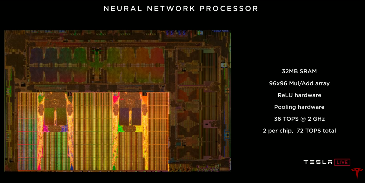
The neural network accelerator itself. There are two of them on the chip. Each of them has 32 megabytes of SRAM for storing temporary results. This minimizes the amount of data we need to transfer to the chip and back, which helps reduce power consumption. Each contains an array of 96x96 multipliers with accumulation, which allows us to do almost 10,000 MUL / ADD operations per clock cycle. There is a dedicated ReLU accelerator, a pooling accelerator. Each of them provides 36 trillion operations per second operating at a frequency of 2 GHz. Two accelerators on a chip give 72 trillion operations per second, which is noticeably higher than the target of 50 trillion.
The video encoder, the video from which we use in the car for many tasks, including displaying the image from the rear-view camera, video registration, and also for recording data in the cloud, Stewart and Andrei will tell about this later. On the chip is a rather modest graphics processor. It supports 32-bit and 16-bit floating point numbers. Also 12 general purpose 64-bit A72 processors. They operate at a frequency of 2.2 GHz, which is about 2.5 times higher than the performance of the previous solution. The security system contains two processors that operate in lockstep mode. This system makes the final decision whether it is safe to transmit control signals to the vehicle's drives. This is where the two plans merge, and we decide whether it is safe to move forward. And, finally, a security system whose task is to ensure that only software that is cryptographically signed by Tesla is used on this chip.
I told you a lot of different performance indicators, and I think it would be useful to look at the perspective. We will look at the neural network from our (narrow) camera. It takes 35 billion operations. If we use all 12 CPUs to process this network, we can do 1.5 frames per second, which is very slow. It is not enough to drive a car. If we used a 600 GFLOPs GPU for the same network, we would get 17 frames per second, which is still not enough to drive a car with 8 cameras. Our neural network accelerator can produce 2100 frames per second. You can see that the amount of computation in CPU and GPU is negligible compared to the accelerator of the neural network.
Let's talk about the neural network accelerator. Just drink some water. On the left is a drawing of a neural network to give you an idea of what is going on. Data enters at the top and passes through each of the blocks. The data is transmitted along the arrows to the various blocks, which are usually convolutions or reverse convolutions with activation functions (ReLU). Green blocks combine layers. It is important that the data obtained by one block is then used by the next block, and you no longer need it - you can throw it away. So all these temporary data are created and destroyed when passing through the network. There is no need to store them outside the chip in DRAM. Therefore, we only store them in SRAM, and in a few minutes I will explain why this is very important.
If you look at the right side, you will see that in this network of 35 billion operations almost all are convolutions, in fact scalar products, the rest are deconvolution (inverse convolutions), also based on a scalar product, and then ReLU and pooling are relatively simple operations. Therefore, if you develop an accelerator, you focus on the implementation of scalar products based on addition with accumulation and optimize them. But imagine that you accelerate this operation 10,000 times and turn 100% into 0.1%. Suddenly, the ReLU and pooling operations become very significant. Therefore, our implementation includes dedicated accelerators for processing ReLU and pooling.
The chip works in conditions of a limited thermal budget. We had to be very careful about how we burn power. We want to maximize the amount of arithmetic we can do. Therefore, we chose 32 bit integer addition, it consumes 9 times less energy than floating point addition. And we chose 8-bit integer multiplication, which also consumes significantly less energy than other multiplication operations, and probably has enough accuracy to get good results. As for the memory. Turning to external DRAM is about a hundred times more expensive in terms of power consumption than using local SRAM. It is clear that we want to make the most of the local SRAM.
From a management point of view, here are the data that was published in an article by Mark Horowitz, in which he critically examined how much energy is required to execute one instruction on a regular integer processor. And you see that the addition operation consumes only 0.15% of the total power. All the rest is management overhead and so on. Therefore, in our design, we strive to get rid of all this as far as possible. What we are really interested in is arithmetic.

So here is the design that we finished. You can see that the main place in it is 32 megabytes of SRAM, they are to the left, to the right, in the center and below. All calculations are performed in the upper center. Each clock cycle we read 256 bytes of activation data from the SRAM array, 128 bytes of weights from the SRAM array, and we combine them into the 96x96 array, which performs 9000 additions with accumulation per clock at 2 GHz. This is only 36.8 trillion. operations. Now, when we are finished with a scalar product, we unload the data, pass it through the dedicated ReLU block, optionally through pulling, and finally put it into the write buffer, where all the results are aggregated. And then we write 128 bytes per clock back to SRAM. And all this happens continuously. We work with scalar products, while unloading previous results, pulling and writing the results back to memory.If you add it all up to 2 GHz, you will need 1 terabyte per second of SRAM bandwidth to support the work. And iron provides it. One terabyte per second bandwidth per accelerator, two accelerators on a chip - two terabytes per second.
The accelerator has a relatively small set of commands. There is a DMA read operation to load data from memory, a DMA write operation to upload results back to memory. Three instructions of convolutions (convolution, deconvolution, inner-product). Two relatively simple operations are shift and elementwise operation (eltwise). And of course, the stop operation when the calculations are over.
We had to develop a neural network compiler. We took a neural network trained by our development team, in the form in which it was used in the old hardware. When you compile it for use on a new accelerator, the compiler performs fusion of layers, which allows us to increase the number of calculations for each SRAM call. It also performs memory smoothing. We perform padding channels to reduce conflicts between memory banks. Memory allocation also takes into account SRAM banks. This is the case when handling conflicts could be implemented in hardware. But with software implementation, we save on hardware due to some software complexity. We also automatically insert DMA operations so that data arrives for calculations on time, without stopping processing. In the end, we generate codeweights, compress and add CRC checksum for reliability. The neural network is loaded into SRAM at startup and is there all the time.
Thus, to start the network, you specify the address of the input buffer, which contains the new image that has just come from the camera; set the output buffer address; set a pointer to the weight of the network; go. The accelerator "goes into itself" and will consistently pass through the entire neural network, usually for one or two million cycles. Upon completion, you get an interrupt and can postprocess the results.
Turning to the results. We had a goal to meet 100 watts. Measurements on cars that drive with a full stack of autopilot showed that we dissipate 72 watts. This is slightly more than in the previous project, but a significant performance improvement is a good excuse. Of these 72 watts, about 15 watts are consumed in neural networks. The cost of this solution is about 80% of what we paid before. In terms of performance, we took the neural network (narrow) of the camera, which I have already mentioned, with 35 billion operations, we launched it on old equipment and received 110 frames per second. We took the same data and the same network, compiled it for the new FSD computer and, using all four accelerators, we can process 2300 frames per second.
Ilon:I think this is perhaps the most significant slide.
Pete: I have never worked on a project where there was more than 3 performance improvements. So it was pretty fun. Compared to the nvidia Drive Xavier solution, the chip provides 21 trillion. operations, while our FSDC with two chips - 144 trillion. operations.
So, in conclusion, I think that we have created a solution that provides outstanding performance of 144 trillion. operations for processing a neural network. It has outstanding power consumption characteristics. We managed to squeeze all this performance into the heat budget we had. This allows you to implement a solution with duplication. The computer has a moderate cost, and what is really important, FSDC will provide a new level of safety and autonomy in Tesla cars, without affecting their cost and mileage. We all look forward to it.
Ilon: If you have questions about the equipment, ask them right now.
The reason why I asked Pete to do a detailed, much more detailed, than most people would probably appreciate if I was diving into the Tesla FSD computer, is as follows. At first glance, it seems incredible how it could happen that Tesla, which had never designed such chips before, created the best chip in the world. But this is exactly what happened. And not just the best one with a small margin, but the best one with a huge margin. All Tesla produced right now is worth this computer. We switched from the Nvidia solution for S and X about a month ago and switched the Model 3 about ten days ago. All cars produced have all the necessary hardware and everything you need for fully autonomous driving. I will say it again: all Tesla cars produced now,have everything you need for full autonomous driving. All you need to do is improve the software. Later today you will be able to ride in cars with a version for developers of improved software for autonomous driving. You will see for yourself. Questions
Q: Do you have the ability to use activation functions other than ReLU?
Pete: Yes, we have a sigmoid, for example
Q: maybe it was worth switching to a more compact process technology, maybe 10 nm or 7 nm?
Pete: At the time when we started to design, not all IPs we wanted to purchase were available at 10 nm
Ilon: It is worth noting that we completed this design about a year and a half ago and started the next generation. Today we are not talking about the next generation, but we are halfway there. All that is obvious for the next generation chip, we do.
Q: The computer is designed to work with cameras. Can I use it with lidar?
Ilon:Lidar is a disastrous decision, and anyone who relies on a lidar is doomed. Doomed. Expensive. Dear sensors that are not needed. It's like having a bunch of expensive unnecessary apps. One small is nothing, but a bunch is already a nightmare. This is stupid, you will see.
Q: Can you assess the impact of energy consumption on mileage?
Pete: For Model 3, target consumption is 250 watts per mile.
Ilon:Depends on the nature of driving. In the city, the effect will be much greater than on the highway. You drive in the city for an hour and you have a hypothetical solution that consumes 1 kW. You will lose 6km on Model 3. If the average speed is 25km / h, then you lose 25%. System consumption has a huge impact on mileage in the city, where we think there will be a large part of the robotaxi market, so power is extremely important.
Q: How reliable are your technologies in terms of IP, are you not going to distribute IP for free?
Pete: We filed dozens of patents for this technology. In fact, this is linear algebra, which I do not think you can patent. (Ilon laughs)
Q:your chip can do something, maybe encrypt all the weights so that your intellectual property remains inside, and nobody could just steal it
Ilon: Oh, I would like to meet a person who can do it. I would hire him in an instant. This is a very difficult problem. Even if you can extract the data, you will need a huge amount of resources to somehow use them.
A big steady advantage for us is the fleet. No one has a fleet. Weights are constantly being updated and improved based on the billions of miles traveled. Tesla has a hundred times more cars with the hardware necessary for training than all the others combined. By the end of this quarter, we will have 500,000 cars with 8 cameras and 12 ultrasonic sensors. In a year we will have over a million cars with FSDC. This is just a huge data advantage. This is similar to how Google has a huge advantage because people use it, and people actually train Google with their queries.
Host:One thing to keep in mind about our FSD computer is that it can work with much more complex neural networks for much more accurate image recognition. It's time to talk about how we actually get these images and how we analyze them. We have a senior director of AI here, Andrei Karpaty, who will explain all this to you. Andrei is a PhD from Stanford University, where he studied computer science with an emphasis on recognition and deep learning.
Ilon: Andrei, why don't you just start, come on. Many doctors came out of Stanford, it doesn’t matter. Andrei teaches a computer vision course at Stanford, this is much more important. Please tell about yourself.
(The translation turned out to be a rather difficult task, I don’t know if I’ll have enough for the second part about the neural network training system, although it seems to be the most interesting for me.)
The presentation text is translated close to the original. Questions to the speaker - selectively with abbreviations.
Host: Hello everyone. Sorry for being late. Welcome to our first day of autonomous driving. I hope we can do this more regularly to keep you informed about our developments.
About three months ago, we were preparing for the fourth quarter earnings report with Ilon and other leaders. I then said that the biggest gap in talking to investors, between what I see inside the company and what its external perception is, is our progress in autonomous driving. And this is understandable, for the last couple of years we have been talking about increasing the production of Model 3, around which there have been many disputes. In fact, a lot was happening in the background.
')
We were working on a new autopilot chip, completely reworked the neural network of computer vision, and finally, we started to release Full Self-Driving Computer (FSDC). We thought it was a good idea to just open the veil, invite everyone and tell us about everything we have been doing for the past two years.
About three years ago we wanted to use, wanted to find the best chip for autonomous driving. We found that there is no chip that was designed from the ground up for neural networks. Therefore, we invited my colleague Pete Bannon, vice president of integrated circuit design, to develop such a chip for us. He has about 35 years of experience in chip design. Including 12 years in the company PASemi, which was later acquired by Apple. He worked on dozens of different architectures and implementations, and was chief designer of the Apple iPhone 5, just before joining Tesla. We are also joined by Ilon Mask. Thank.
Ilon: Actually, I was going to introduce Pete, but since this has already been done, I will add that he is simply the best architect of systems and integrated circuits in the world I know. It is an honor that you and your team at Tesla. Please just tell us about the incredible work you have done.
Pete: Thanks Ilon. I am pleased to be here this morning and really pleased to tell you about all the work that my colleagues and I have done here at Tesla over the past three years. I will tell you a little about how it all started, and then I will introduce you to the FSDC computer and tell you a little how it works. We delve into the chip itself and look at some of the details. I will describe how the specialized neural network accelerator that we designed works, and then I will show some results, and I hope that by that time you will not fall asleep.
I was hired in February 2016. I asked Ilona if he was ready to spend as much as needed to create this specialized system, he asked: "We will win?", I answered: "Well, yes, of course," then he said, "I'm in business" and so it all started . We hired a bunch of people and started thinking about how a chip designed specifically for fully autonomous driving would look. We spent eighteen months developing the first version, and in August 2017 released it for production. We got the chip in December, it earned, and actually it worked very well on the first try. In April 2018, we made several changes and released version B zero Rev. In July 2018, the chip was certified, and we started full-scale production. In December 2018, the autonomous driving stack started working on new equipment, and we were able to start re-equipment of official cars and testing in the real world. In March 2019 we started installing a new computer in models S and X, and in April in Model 3.
So, the whole program, from hiring the first employees to a full launch in all three models of our cars, took a little more than three years. This is probably the fastest system development program I've ever participated in. And it actually speaks of the benefits of high vertical integration, allowing you to perform parallel design and speed up deployment.
In terms of goals, we were completely focused solely on the requirements of Tesla, and this makes life much easier. If you have a single client, you do not need to worry about others. One of the goals was to keep the power below 100 W so that we could retrofit existing machines. We also wanted to reduce the cost to provide redundancy for greater security.
At a time when we poked our finger at the sky, I argued that driving a neural network would require at least 50 trillion operations per second to drive a car. Therefore, we wanted to get at least that much, and better more. Package size (batch) determines the number of items with which you work simultaneously. For example, Google’s TPU has a packet size of 256, and you need to wait until you have 256 items to process before you can start working. We didn’t want to wait and developed our single size package engine. As soon as the image appears, we process it immediately to minimize latency and increase security.
We needed a graphics processor to do some post-processing. At first, it took quite a lot, but we assumed that over time it would become less, as neural networks become better and better. And it really happened. We risked putting a fairly modest graphics processor into the design, and it turned out to be a good idea.
Security is very important, if you do not have a secure car, you cannot have a safe car. Therefore, much attention is paid to security and, of course, security.
From the point of view of the chip architecture, as Ilon mentioned earlier, in 2016 there was no accelerator originally created for neural networks. Everyone just added instructions to their CPU, GPU or DSP. Nobody did the development from 0. Therefore, we decided to do it ourselves. For other components, we purchased standard IP industrial CPUs and GPUs, which allowed us to reduce development time and risks.
Another thing that was a bit unexpected for me was the ability to use existing commands in Tesla. Tesla had excellent power supply design teams, signal integrity analysis, chassis design, firmware, system software, board design, and a really good system validation program. We could use all this to speed up the program.
This is how it looks. On the right you see the connectors for the video coming from the car’s cameras. Two computers autonomous driving in the center of the board, on the left - the power supply and control connectors. I love when the decision comes down to its basic elements. You have a video, calculator and power, simple and clear. Here is the previous Hardware 2.5 solution, which the computer went into, and which we installed over the last two years. Here is the new design for the FSD computer. They are very similar. This, of course, is due to the limitations of the car modernization program. I would like to point out that this is actually a rather small computer. It is placed behind the glove compartment, and does not take up half the trunk.
As I said earlier, there are two completely independent computers on the board. They are highlighted in blue and green. On the sides of each SoC, you can see DRAM chips. Below on the left you see FLASH chips that represent the file system. Here are two independent computers that are loaded and run under their own operating system.
Ilon: The general principle is that if some part fails, the machine will be able to continue. The camera, the power supply circuit, one of Tesla's computer chips fails - the car keeps moving. The probability of failure of this computer is significantly lower than the probability that the driver will lose consciousness. This is a key indicator, at least in order.
Pete: Yes, so one of the things we do to keep the computer running is redundancy of power sources. The first chip works on one power supply, and the second on the other. The same is true for cameras, half of the cameras work on the power supply marked in blue, the other half on green. Both chips get all the video and process it independently.
From the point of view of driving, the sequence is to collect a lot of information from the world around you, we have not only cameras, but also a radar, GPS, maps, a gyrostabilizer (IMU), ultrasonic sensors around the car. We have the steering angle, we know what the acceleration of the car should be. It all comes together to form a plan. When the plan is ready, the two computers exchange their versions of the plan to make sure they match.
Assuming that the plan coincided, we issue control signals and drive the car. Now, when you move with the new control, you certainly want to check it out. We verify that the transmitted control signals coincide with what we intended to transfer to the actuators in the car. Sensors are used to verify that control is in effect. If you ask the car to accelerate, or brake, or turn right or left, you can look at the accelerometers and see if this really happens. There is significant redundancy and duplication of both our data and our ability to monitor data.
We proceed to talk about the chip. It is packed in 37.5 mm BGA with 1600 contacts, most of which are power and earth. If you remove the cover, you can see the substrate and the crystal in the center. If you separate the crystal and turn it over, you will see 13,000 C4 contacts (bumps) scattered over the surface. Below are the twelve metal layers of the integrated circuit. This is a 14-nanometer FinFET CMOS process with a size of 260 mm.kv., this is a small scheme. For comparison, the usual cell phone chip is about 100 mm.kv. A high-performance graphics processor will be about 600-800 mm.kv. So we are like in the middle. I would call it the golden mean, this is a convenient size for assembly. There are 250 million logic elements and 6 billion transistors here, which, although I’m working on it all this time, just amaze me. The chip is manufactured and tested in accordance with the AEC Q100 automotive standard.
I would just like to bypass the chip and explain all its parts. I will go in the same order as the pixel coming from the camera. In the upper left corner you can see the camera interface. We can accept 2.5 billion pixels per second, which is more than enough for all available sensors. A network that distributes data from the memory system to the memory controllers on the right and left edges of the chip. We use standard LPDDR4, operating at a speed of 4266 gigabits per second. This gives us a maximum bandwidth of 68 gigabytes per second. This is a pretty good bandwidth, but not excessive, we are trying to stay in the middle. The image processor has a 24-bit internal pipeline, which allows us to make full use of the HDR sensors that are in the car. It performs advanced Tone mapping, which helps to better highlight details and shadows, as well as advanced noise reduction, which simply improves the overall quality of the images we use in the neural network.
The neural network accelerator itself. There are two of them on the chip. Each of them has 32 megabytes of SRAM for storing temporary results. This minimizes the amount of data we need to transfer to the chip and back, which helps reduce power consumption. Each contains an array of 96x96 multipliers with accumulation, which allows us to do almost 10,000 MUL / ADD operations per clock cycle. There is a dedicated ReLU accelerator, a pooling accelerator. Each of them provides 36 trillion operations per second operating at a frequency of 2 GHz. Two accelerators on a chip give 72 trillion operations per second, which is noticeably higher than the target of 50 trillion.
The video encoder, the video from which we use in the car for many tasks, including displaying the image from the rear-view camera, video registration, and also for recording data in the cloud, Stewart and Andrei will tell about this later. On the chip is a rather modest graphics processor. It supports 32-bit and 16-bit floating point numbers. Also 12 general purpose 64-bit A72 processors. They operate at a frequency of 2.2 GHz, which is about 2.5 times higher than the performance of the previous solution. The security system contains two processors that operate in lockstep mode. This system makes the final decision whether it is safe to transmit control signals to the vehicle's drives. This is where the two plans merge, and we decide whether it is safe to move forward. And, finally, a security system whose task is to ensure that only software that is cryptographically signed by Tesla is used on this chip.
I told you a lot of different performance indicators, and I think it would be useful to look at the perspective. We will look at the neural network from our (narrow) camera. It takes 35 billion operations. If we use all 12 CPUs to process this network, we can do 1.5 frames per second, which is very slow. It is not enough to drive a car. If we used a 600 GFLOPs GPU for the same network, we would get 17 frames per second, which is still not enough to drive a car with 8 cameras. Our neural network accelerator can produce 2100 frames per second. You can see that the amount of computation in CPU and GPU is negligible compared to the accelerator of the neural network.
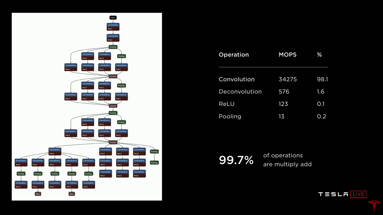
Let's talk about the neural network accelerator. Just drink some water. On the left is a drawing of a neural network to give you an idea of what is going on. Data enters at the top and passes through each of the blocks. The data is transmitted along the arrows to the various blocks, which are usually convolutions or reverse convolutions with activation functions (ReLU). Green blocks combine layers. It is important that the data obtained by one block is then used by the next block, and you no longer need it - you can throw it away. So all these temporary data are created and destroyed when passing through the network. There is no need to store them outside the chip in DRAM. Therefore, we only store them in SRAM, and in a few minutes I will explain why this is very important.
If you look at the right side, you will see that in this network of 35 billion operations almost all are convolutions, in fact scalar products, the rest are deconvolution (inverse convolutions), also based on a scalar product, and then ReLU and pooling are relatively simple operations. Therefore, if you develop an accelerator, you focus on the implementation of scalar products based on addition with accumulation and optimize them. But imagine that you accelerate this operation 10,000 times and turn 100% into 0.1%. Suddenly, the ReLU and pooling operations become very significant. Therefore, our implementation includes dedicated accelerators for processing ReLU and pooling.
The chip works in conditions of a limited thermal budget. We had to be very careful about how we burn power. We want to maximize the amount of arithmetic we can do. Therefore, we chose 32 bit integer addition, it consumes 9 times less energy than floating point addition. And we chose 8-bit integer multiplication, which also consumes significantly less energy than other multiplication operations, and probably has enough accuracy to get good results. As for the memory. Turning to external DRAM is about a hundred times more expensive in terms of power consumption than using local SRAM. It is clear that we want to make the most of the local SRAM.
From a management point of view, here are the data that was published in an article by Mark Horowitz, in which he critically examined how much energy is required to execute one instruction on a regular integer processor. And you see that the addition operation consumes only 0.15% of the total power. All the rest is management overhead and so on. Therefore, in our design, we strive to get rid of all this as far as possible. What we are really interested in is arithmetic.
So here is the design that we finished. You can see that the main place in it is 32 megabytes of SRAM, they are to the left, to the right, in the center and below. All calculations are performed in the upper center. Each clock cycle we read 256 bytes of activation data from the SRAM array, 128 bytes of weights from the SRAM array, and we combine them into the 96x96 array, which performs 9000 additions with accumulation per clock at 2 GHz. This is only 36.8 trillion. operations. Now, when we are finished with a scalar product, we unload the data, pass it through the dedicated ReLU block, optionally through pulling, and finally put it into the write buffer, where all the results are aggregated. And then we write 128 bytes per clock back to SRAM. And all this happens continuously. We work with scalar products, while unloading previous results, pulling and writing the results back to memory.If you add it all up to 2 GHz, you will need 1 terabyte per second of SRAM bandwidth to support the work. And iron provides it. One terabyte per second bandwidth per accelerator, two accelerators on a chip - two terabytes per second.
The accelerator has a relatively small set of commands. There is a DMA read operation to load data from memory, a DMA write operation to upload results back to memory. Three instructions of convolutions (convolution, deconvolution, inner-product). Two relatively simple operations are shift and elementwise operation (eltwise). And of course, the stop operation when the calculations are over.
We had to develop a neural network compiler. We took a neural network trained by our development team, in the form in which it was used in the old hardware. When you compile it for use on a new accelerator, the compiler performs fusion of layers, which allows us to increase the number of calculations for each SRAM call. It also performs memory smoothing. We perform padding channels to reduce conflicts between memory banks. Memory allocation also takes into account SRAM banks. This is the case when handling conflicts could be implemented in hardware. But with software implementation, we save on hardware due to some software complexity. We also automatically insert DMA operations so that data arrives for calculations on time, without stopping processing. In the end, we generate codeweights, compress and add CRC checksum for reliability. The neural network is loaded into SRAM at startup and is there all the time.
Thus, to start the network, you specify the address of the input buffer, which contains the new image that has just come from the camera; set the output buffer address; set a pointer to the weight of the network; go. The accelerator "goes into itself" and will consistently pass through the entire neural network, usually for one or two million cycles. Upon completion, you get an interrupt and can postprocess the results.
Turning to the results. We had a goal to meet 100 watts. Measurements on cars that drive with a full stack of autopilot showed that we dissipate 72 watts. This is slightly more than in the previous project, but a significant performance improvement is a good excuse. Of these 72 watts, about 15 watts are consumed in neural networks. The cost of this solution is about 80% of what we paid before. In terms of performance, we took the neural network (narrow) of the camera, which I have already mentioned, with 35 billion operations, we launched it on old equipment and received 110 frames per second. We took the same data and the same network, compiled it for the new FSD computer and, using all four accelerators, we can process 2300 frames per second.
Ilon:I think this is perhaps the most significant slide.
Pete: I have never worked on a project where there was more than 3 performance improvements. So it was pretty fun. Compared to the nvidia Drive Xavier solution, the chip provides 21 trillion. operations, while our FSDC with two chips - 144 trillion. operations.
So, in conclusion, I think that we have created a solution that provides outstanding performance of 144 trillion. operations for processing a neural network. It has outstanding power consumption characteristics. We managed to squeeze all this performance into the heat budget we had. This allows you to implement a solution with duplication. The computer has a moderate cost, and what is really important, FSDC will provide a new level of safety and autonomy in Tesla cars, without affecting their cost and mileage. We all look forward to it.
Ilon: If you have questions about the equipment, ask them right now.
The reason why I asked Pete to do a detailed, much more detailed, than most people would probably appreciate if I was diving into the Tesla FSD computer, is as follows. At first glance, it seems incredible how it could happen that Tesla, which had never designed such chips before, created the best chip in the world. But this is exactly what happened. And not just the best one with a small margin, but the best one with a huge margin. All Tesla produced right now is worth this computer. We switched from the Nvidia solution for S and X about a month ago and switched the Model 3 about ten days ago. All cars produced have all the necessary hardware and everything you need for fully autonomous driving. I will say it again: all Tesla cars produced now,have everything you need for full autonomous driving. All you need to do is improve the software. Later today you will be able to ride in cars with a version for developers of improved software for autonomous driving. You will see for yourself. Questions
Q: Do you have the ability to use activation functions other than ReLU?
Pete: Yes, we have a sigmoid, for example
Q: maybe it was worth switching to a more compact process technology, maybe 10 nm or 7 nm?
Pete: At the time when we started to design, not all IPs we wanted to purchase were available at 10 nm
Ilon: It is worth noting that we completed this design about a year and a half ago and started the next generation. Today we are not talking about the next generation, but we are halfway there. All that is obvious for the next generation chip, we do.
Q: The computer is designed to work with cameras. Can I use it with lidar?
Ilon:Lidar is a disastrous decision, and anyone who relies on a lidar is doomed. Doomed. Expensive. Dear sensors that are not needed. It's like having a bunch of expensive unnecessary apps. One small is nothing, but a bunch is already a nightmare. This is stupid, you will see.
Q: Can you assess the impact of energy consumption on mileage?
Pete: For Model 3, target consumption is 250 watts per mile.
Ilon:Depends on the nature of driving. In the city, the effect will be much greater than on the highway. You drive in the city for an hour and you have a hypothetical solution that consumes 1 kW. You will lose 6km on Model 3. If the average speed is 25km / h, then you lose 25%. System consumption has a huge impact on mileage in the city, where we think there will be a large part of the robotaxi market, so power is extremely important.
Q: How reliable are your technologies in terms of IP, are you not going to distribute IP for free?
Pete: We filed dozens of patents for this technology. In fact, this is linear algebra, which I do not think you can patent. (Ilon laughs)
Q:your chip can do something, maybe encrypt all the weights so that your intellectual property remains inside, and nobody could just steal it
Ilon: Oh, I would like to meet a person who can do it. I would hire him in an instant. This is a very difficult problem. Even if you can extract the data, you will need a huge amount of resources to somehow use them.
A big steady advantage for us is the fleet. No one has a fleet. Weights are constantly being updated and improved based on the billions of miles traveled. Tesla has a hundred times more cars with the hardware necessary for training than all the others combined. By the end of this quarter, we will have 500,000 cars with 8 cameras and 12 ultrasonic sensors. In a year we will have over a million cars with FSDC. This is just a huge data advantage. This is similar to how Google has a huge advantage because people use it, and people actually train Google with their queries.
Host:One thing to keep in mind about our FSD computer is that it can work with much more complex neural networks for much more accurate image recognition. It's time to talk about how we actually get these images and how we analyze them. We have a senior director of AI here, Andrei Karpaty, who will explain all this to you. Andrei is a PhD from Stanford University, where he studied computer science with an emphasis on recognition and deep learning.
Ilon: Andrei, why don't you just start, come on. Many doctors came out of Stanford, it doesn’t matter. Andrei teaches a computer vision course at Stanford, this is much more important. Please tell about yourself.
(The translation turned out to be a rather difficult task, I don’t know if I’ll have enough for the second part about the neural network training system, although it seems to be the most interesting for me.)
Source: https://habr.com/ru/post/450500/
All Articles