RAM Expansion Board for Apple IIgs
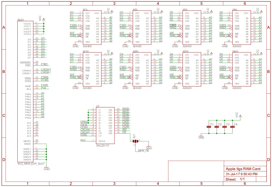
The proposed RAM expansion card for the Apple IIgs computer is made on NEC uPD424400-70 microcircuits from several 1-MB SIMM-modules. Each of these microcircuits stores 1 M nibbytes and is located in a 26-pin SOJ package.
The Apple IIgs computer is made on a 65C816 processor - 16-bit, but with an 8-bit data bus. Expansion card contains 4 MB of RAM. The memory is divided into four lines, 1 MB each. The line consists of two 1 M nibble microcircuits, thus, all it took was eight microcircuits.
The slot for the expansion card of the RAM at the computer already is. All the necessary signals are displayed on it, the computer also takes over the regeneration of the dynamic RAM. Therefore, the expansion card turned out quite simple. The author decided to make the board small-sized, since the cost of its manufacture depends on it, and also to place all the logic in the FPGA GAL22V10.
')
The following signals are present on the RAM expansion slot:
FRA0-FRA9 - 10-bit multiplexed cell address, fed directly to the address inputs of dynamic RAM chips
CROW0, 1 - two bits to select one of four lines
/ CRAS - dynamic RAM address line gating signal
/ CCAS - dynamic RAM column address gating signal
FR / W - write resolution in RAM, this signal requires additional processing, see below.
D0-D7 - data bus, connects directly to the I / O lines of RAM chips
/ CSEL - a logical unit appears on this line when reading from RAM, it must be inverted and fed to the inputs / OE of RAM microcircuits
MSIZE - informs the computer of the line size: unit - 256 kB, zero - 1 MB, here this line is connected to the common wire
14M, PH2CLK, A10-A15 - are not involved in the proposed board
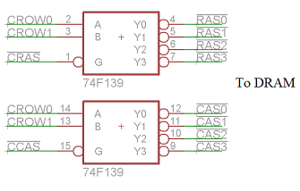
The signals / CRAS and / CCAS need to be demultiplexed to get separate signals / RAS and / CAS for each of the lines. For this, the 74F139 chip is suitable (hereinafter it is assumed that there will be no separate chips on the board, instead of them there will be one common FPGA).
The FR / W signal cannot be fed directly to the / WE input of the dynamic RAM chips, and here's why. With a normal read-write operation, the / RAS line first becomes active (which corresponds to a logical zero), then the / CAS line becomes active. During the cycle of regeneration of dynamic RAM, on the contrary, the / CAS line, then / RAS line becomes active first. But the applied chips require that a unit appear on the / WE line before the / RAS line becomes active. And the FR / W signal from Apple IIgs does not comply with this requirement. The state of FR / W during the regeneration cycle is undefined. Therefore, a circuit is required that detects the regeneration cycle and feeds the unit to / WE.
The first step is to identify the regeneration cycle. Below is a timeline:
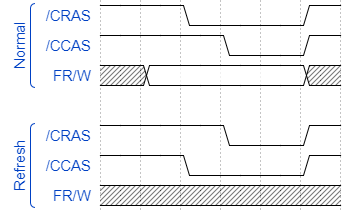
The idea of the author is to use a "transparent" latch. The signal / CRAS for it is the input, / CCAS - the click signal. When the unit is on the / CCAS unit, the device passes through the input signal through: the state of the output changes after the state of the input. At the moment of transition / CCAS from one to zero, the latch remembers the signal at the input, and now it does not change at the output. In a typical read / write operation on / CRAS, there is zero at the time of switching / CCAS from one to zero. And during the regeneration cycle on / CRAS, there is a unit also at the moment of switching / CCAS to zero. Then, when / CCAS switches back to one, the latch again becomes “transparent”. It resembles a fantastic flower from the "Secrets of the Third Planet", which can be both a "mirror" and a "camera".

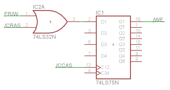
At the beginning, the author made the following scheme:
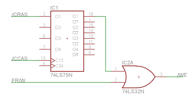
But for its transfer to the FPGA GAL22V10 will require two output output. Therefore, the scheme had to be simplified. In normal operation, the FR / W signal takes on the desired value before it clicks, so this is also possible.
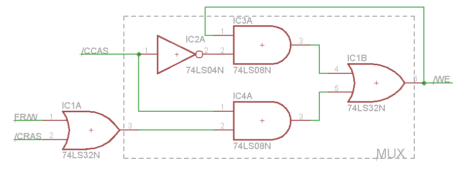
A “transparent” latch can be made from a multiplexer, and it, in turn, from logical elements. The scheme becomes:
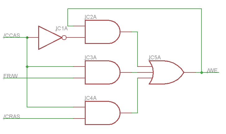
And after simplification - this:
This option is transferred to the FPGA. To compile the author applied WinCUPL. This program is on the Atmel website. She is raw and constantly crashes, but coped with the task perfectly. Programmer - Genius G540.
The jumper SJ1 on the board operates as follows. If pins 1 and 2 are connected, the / OE signal passes through the FPGA. If pins 2 and 3 are connected, it is connected to the common wire. The author was not sure that the scheme for detecting the regeneration cycle will work. Therefore, he added this jumper in case the FPGA configuration has to be redone.
Since it turned out that everything works, no need to solder the pins, just connect pins 1 and 2 with a drop of solder.
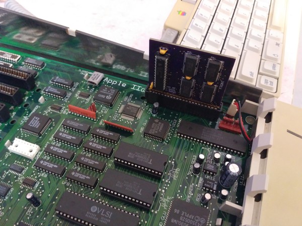
To reduce the size of the board, the author applied one power capacitor for every four RAM chips, and the chips themselves placed on both sides of the board.
Chips in SOJ packages are difficult to solder, and especially - to solder with a soldering iron. The author recommends using a hair dryer.
Correctly deploy ICs. On the bottom line, they are inverted. Pin 1 looks down.
Some through holes are too close to the pads. Do not solder them together.
And pads 1 and 2 for the jumper, on the contrary, close.
C1 - C3 capacitors have a capacitance of 0.1 microfarad, C4 - 10 microfarad.
The author ordered the fees on OSH Park. Applied coating ENIG - gold, but very thin. For game cartridges is not good - quickly erased. And here the board was placed in the slot once and is not removed from there anymore.
The author thanks GGLabs for the scheme of a similar board, it really helped, thanks!
The finished scheme turned out like this:
Files:
Firmware FPGA GAL22V10 , applied program WinCUPL version 5.30.4
Board , applied program Eagle version 7.1
Scheme in PDF
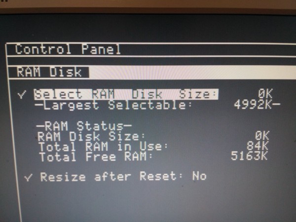
Earned!
Source: https://habr.com/ru/post/450374/
All Articles