How does the Philips VideoWRITER. First pictures of iron, then a bit of bore
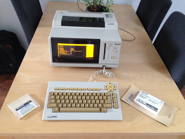
VideoWRITER device for editing and printing texts was released by Philips in 1985. It is made on a Z80-compatible processor and contains 16 KB of ROM and the same amount of RAM (as it later turned out, the ROM is larger). To save documents, it has a 3.5-inch drive. Become the happy owner of this "combine" (there is also a built-in printer) could have been for 799 dollars.
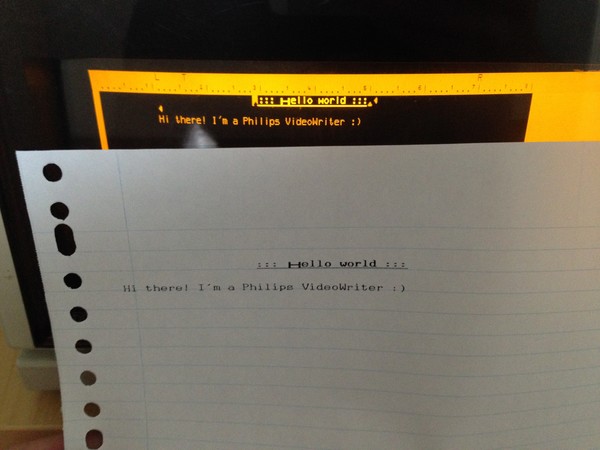
The screen of the orange CRT monitor is noticeably wider than usual. Not only the window with the document being edited is placed on it, but also the menu to its right. There are also hints, including the appointment of function keys. The document is always displayed in light characters on a dark background, the menu is vice versa. In the lower left corner of the overlay on the screen marked: DDS - Dual Display Screen ...
')
The editor is pretty straightforward; don't even expect Comic Sans. The font is only one, standard attributes are available: bold, italic, underlined, upper and lower indices. And standard text alignment methods. There is also a ruler and line feed characters.
The printer prints on ordinary A4 sheets using thermal transfer. If there is no special cartridge, according to the Wikipedia article , you can print on thermal paper. The author was very surprised that the device still prints after so many years spent in a hot attic.
The keyboard is compact, but typing on it is convenient. Special keys on it allow you to switch font attributes, cancel actions and check spelling, if there is a diskette with a dictionary. The keyboard is connected with an RJ14 connector - the essence is the same as that of RJ11 and RJ45.
Documents are stored on 3.5-inch floppy disks. When turned on, the machine immediately searches for a floppy disk, and if it cannot “understand” what is there, it offers to format it. Most likely, the format is incompatible with that used on the PC. And how many kilobytes fit there, 360 or 720?
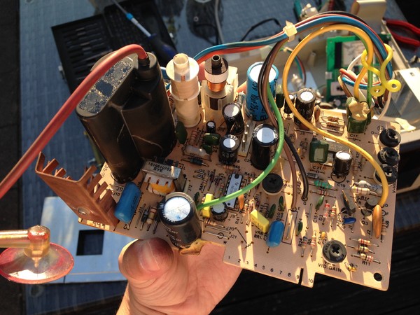
And now it's time to lift the top cover and see what is under it. First of all, just consider the board, while not delving into their device. First, discharge the kinescope. We take the screwdriver, pre-connected to the common wire with the help of a "crocodile", and, holding it by the insulating handle, slip the sting under the suction cup. Although it is written on the kinescope itself: do not discharge the arc discharge, connect a high-resistance voltmeter between the anode and the chassis. And, like, everything is discharged gradually. Perhaps the TDX is "gentle."
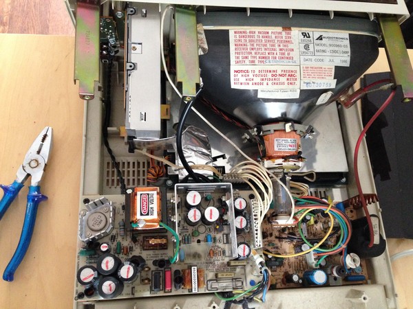
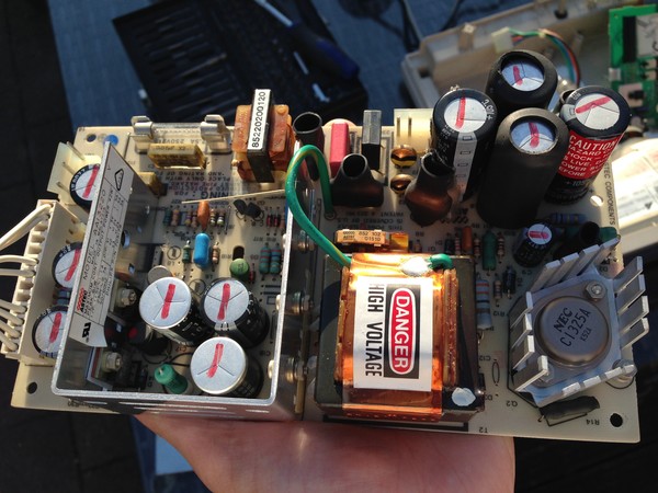
To remove the power supply, you need to unscrew the two screws. Now the author is shooting this BP a second time. The first was when a capacitor burst in it, there was a lot of smoke, but the author found the same one, soldered it, and it all worked. It was not an electrolytic capacitor, but one that was rectangular, from the top in the middle. Which is now red.
The monitor board is very small compared to other similar boards of those years. Even the CRT board is not there - just a socket (which is not uncommon in monochrome monitors). The board has several settings, as well as a 10-pin connector for connecting to the motherboard. I wonder what's behind the cap? And why chip 556 - two 555 timers in one package? Generators "saw" immediately for personnel and lower case developments?
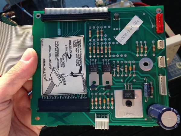
The printer board is located directly under the printer itself. From it comes a cable to the motherboard, as well as cables to the engines, paper push buttons, contrast adjuster for printing, the print head, the trailers and the paper sensor.
The motherboard is shielded from all sides. Only two ROM chips have a square hole in the screen:
Remove the screen and see what is interesting on the motherboard.
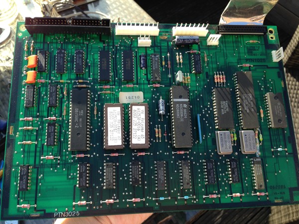
D8156HC-2 - I / O controller. Presumably, controls the printer, as it is located near the printer connector in the upper left corner. The microcircuit contains three ports: two 8-bit and one 6-bit, 14-bit timer and 256 bytes of static RAM. We'll see later what each of the ports is for, and whether or not the chip actually controls the printer. It is also likely to "communicate" with the keyboard. The chip uses a combined address and data bus. It turned out the microprocessor - too.
HN27C256-20 - 32 kilobyte ROM with 8-bit data bus width. There are two such chips, it turns out 64 kilobytes. So, Wikipedia incorrectly states that the ROM is only 16 kilobytes. Well, the ROM will occupy the entire 64-kilobyte address space Z80? And there after all also 16 kilobyte of the RAM. So, there is some sort of page switching. Also see ...
NSC800N-3I - microprocessor. With the Z80, it is only compatible, and the pinout is completely different. On the left is just an amazing combined address and data bus. The lower 8 bits of the address bus are also used as a data bus. And to distinguish the address from the data, there is an output of ALE. One means that on these lower eight bits is part of the address. And on the right - only signals. The same ALE, as well as Read Enable, Write Enable, the choice between memory and ports, and so on. Of course, it’s harder to work with such a microprocessor than with a regular Z80 or its clone. It works, according to the datasheet, at a frequency of up to 2.5 MHz, which means that the frequency of 5 MHz quartz is somewhere divided into two. Compare the caps of this non-standard processor and the usual Z80:
HM48416AP-15 is a dynamic RAM of 16 kilopoly bytes. Two such chips form 16 kilobyte RAM.
WD1770-PH is a Western Digital drive controller. Minimum of external components, compatibility with various data storage formats on a diskette. In general, does not need advertising.
NCR 7250 PY - video controller? It looks like it, because there is nothing else pretending to this function on the board.
HM6116-4 - static RAM for 2 kilobytes. In general, video memory. The video mode here is only text, so no more is needed. Although ... Immediately not 80x25, here the line is wider than 80 characters, plus attributes. Well, that means it fits.
So, we found out that the machine has 16 kilobytes of RAM and 64 kilobytes of ROM, and page switching should be implemented somewhere. Take a walk on the board with a multimeter and draw everything we see.
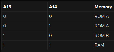
First, look for the Chip Select signals. Let's start with the output / CE of that ROM chip, in which the letter A is printed on the sticker. It turns out that it is connected to the output of element I. So, where are its inputs going? To the two outputs of the chip 74139, containing two decoders with two inputs and four outputs. We are only one of them interested in:

A14 and A15 signals come from the microprocessor to its inputs, so the memory is divided into four blocks of 16 kilobytes. The / M (memory select) signal is sent to the / E (enable) input from the microprocessor, so the 74139 chip is active when the microprocessor requires memory access. It turns out, the distribution of the address space is. ROM “A” is selected when at 74139 the unit is either at the output / Q0 or at the output / Q1, ROM is at the “B” unit at 1 / Q2, RAM is at 1 / Q3. But with RAM, too, is not so simple, then we'll figure it out. So, what is selected for different combinations of signals on the A14 and A15:
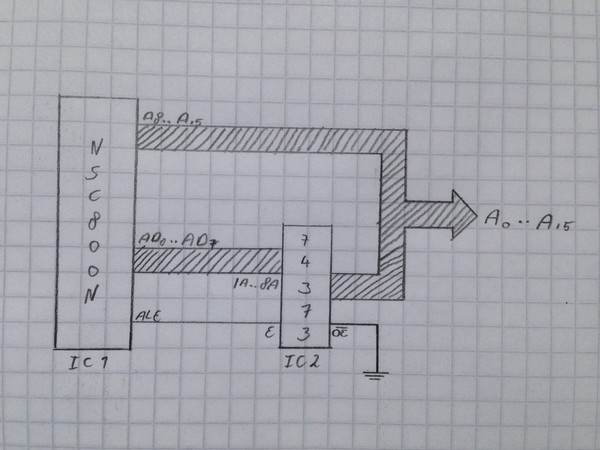
Go to the address bus. As we have already found out, everything is more complicated there than in systems with the usual Z80. It turns out that in order to separate the address from the data, the 8-bit latch 74373 is applied here. Its data inputs are connected to the AD0 - AD7 lines, and the latching input is connected to the ALE line. When a unit appears on ALE, the lower half of the address is written to 74373. And the / OE input is always connected to the common wire.
Further, the “address bus” will be considered the output lines 74373 in combination with the upper lines of the address bus itself, where data is never present. Well, the picture shows everything:
Now let's see how the ROM chips are connected. With the connection of ROM "A" nothing unusual is observed. Just the line A0 - A14 of the previously considered “pure address” bus (after 74373). Only A0 - A13 lines are connected to ROM “B”. And what about the A14? Maybe this line goes to the common wire or power supply, and half the capacity is not used? Not. It goes to output 39 (PC2) of the A8156 I / O controller. That's all it became clear with switching pages. The halves of the ROM “B” can be switched by software.
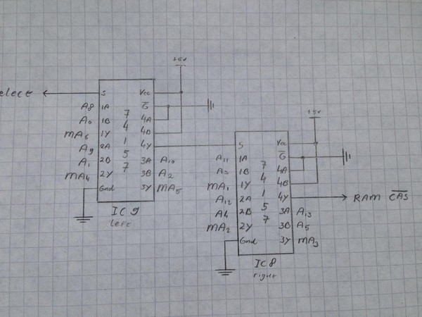
RAM, as we found out, is performed on two chips of dynamic RAM 16 kilo-bytes each. Each byte of RAM is stored in two chips at once, one nibble in the first, the other in the second.
To select an address, you must first select a row, then a column. For this, two 74157 microcircuits are used - four data selectors with two inputs and one output. Now back to the first scheme. In addition to the output / WR, there is another output that goes to the input selection of the first chip 74157. When on / Q3 is zero, the row address is selected, and when there is one - the column address:
Walking through the printed conductors, the author found out that only six of the eight outputs of two 74157 microcircuits are used as addresses MA1 - MA6 for RAM microcircuits. And the MA0 and MA7 lines are connected directly to the address bus A6 and A7 lines. Chips 48416 have eight rows and six columns, so you only need to switch six lines, the other two can be connected directly to the address bus lines, since they do not affect the choice of the column.
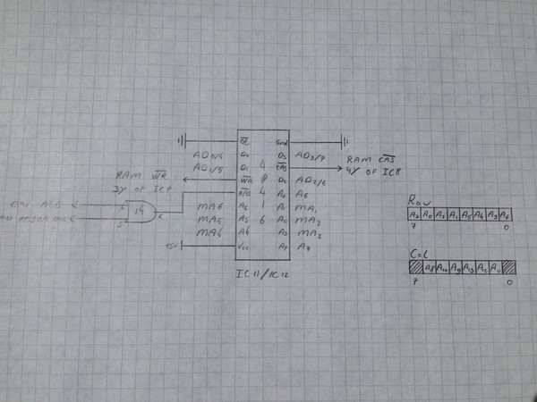
The order of connecting lines to the address bus does not follow any logic. But it works. Maybe it was just easier to design a board?
It is also interesting how the 74157 chips are cascaded: the 4Y output first goes to the second selection input, and the second 4Y output goes to the / CAS line:
Unlike ROM, dynamic RAM does not have a separate line / CE. As the author understood, these microcircuits provide reading or writing, when the / CAS is zero. Well, that's the way it is: zero on / Q3 means zero on / CAS. The address of the RAM line is formed when the ALE line is zero and when the microprocessor is not reset.
With the address space figured out, move on to the periphery. The author still went through the board with a multimeter and got the following scheme:
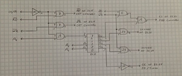
The upper left shows where the / RD and / WR signals for the video controller (VDP) come from. Please note that chip select is not visible for VDP. This means that the only signal similar to / CS for the video controller is the ALE signal from the microprocessor. It turns out that the video controller receives data in general about all I / O operations. We will not concentrate on this, let's see what is there with the other I / O devices.
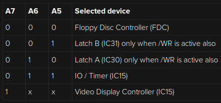
The remaining I / O addresses are decrypted by the second half of the 74139 chip, the same half of which switches the pages of the address space. This descrambler is selected when an input-output operation is performed, and on A7 it is zero. It seems that the A7 line is responsible for the choice between the video controller and the rest of the periphery. A6 and A5 determine which device will be selected by the decoder:
Can A7 be a chip select line for a video controller, and is it selected when there is one? Without a datasheet on the NCR 7250, it cannot be determined, but it is quite plausible if the effect of the ALE line on the video controller is not implemented as something quite unusual.
Further, the author conducted a reverse-engineering of connecting the microprocessor signal lines:
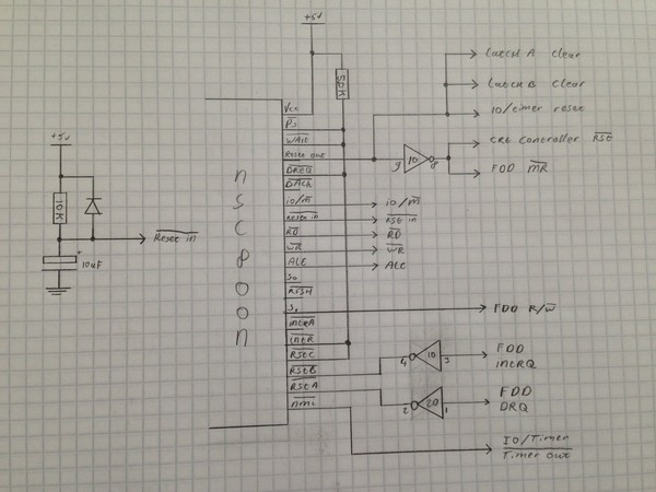
The same diagram shows the method for generating a reset signal. When turned on, the capacitor is charged with a delay; when it is turned off, it discharges quickly. The reset / RESET IN signal is inverse, it goes to the microprocessor, and it generates a direct RESET OUT signal to reset various peripherals.
The line of nonmaskable interrupts / NMI works the same as on a regular Z80. When interrupts are enabled, a zero on this line invokes the interrupt handling routine at address 0x66. In this case, the / NMI signal comes from the output of timer IC25. An interrupt occurs on every overflow of this timer.
The NSC800N microprocessor also has an / INTR input, with zero on which the transition to the address 0x38 occurs, but this input is not used in VideoWRITER.
There are also three restart signals / RSTA, / RSTB and / RSTC, causing the transition, respectively, to the address 0x3C, 0x34 or 0x2C. Of these, only the first two are involved, and they are controlled by the drive controller. By the / RSTA signal, the drive controller informs the microprocessor about the state of its data register, and the / RSTB signal indicates the completion of the command execution.
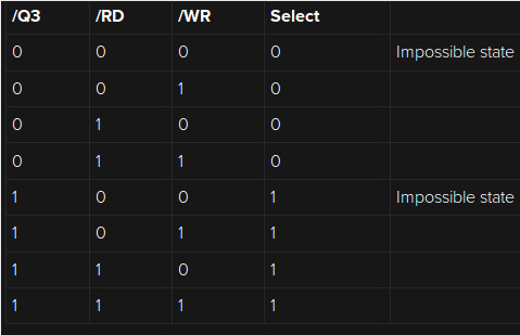
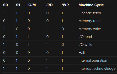
And now about one line - S1. Together with the S0 line, it determines the state of the bus. Thus, the drive controller selects the read or write mode. But why is the S1 line used instead of / RD and / WR only the drive controller? Unclear. The S0, S1 and IO / M lines can be used to choose between read and write modes for memory and peripherals, but using other lines has the same effect. Maybe the developers have tried several options and decided to focus on the method of decoding the read-write mode, which is used in the usual Z80? In any case, according to the datasheet on the NSC800N and the table below, the signal S1 can be a read signal from peripheral devices, but only if there is also a select signal going directly to the device:
The device is in operation, the video was shot by another author - Grr_I'm_Here:
Source: https://habr.com/ru/post/450310/
All Articles