Amateur Radio Technology: Prototype PCB Production in a Chinese Factory
The purpose of the publication : to tell how to make an uncomplicated printed circuit board with minimal time and money.
As it was already written earlier , the work of radio amateurs has a budget limited by the family and has a limit on the time taken from the family. In the fight against these restrictions, hams are assisted by the use of CAD / CAM. Moreover, CAD can be installed on a home computer, and CAM located in another part of the world.
This article describes : how to prepare and download from CAD Eagle 7.7.0 a task in the format Gerber RS274X for a CAM located in the PRC; how to place an order for the manufacture of PCB and its delivery to the Russian Federation.
Formulation of the problem
Non-time production of a prototype PCB at a domestic enterprise takes 4-5 working days and costs 2,823.14 rubles for a payment of 100 * 80 and 1 mm thick with a green solder mask, coated with POS-63 (HASL) contact pads and white silk-screen printing one side. Excluding shipping charges.
It seemed to me a little expensive. As usually happens in such cases, I turned for good advice to my colleagues, who told me that they were ordering similar printed circuit boards for their amateur projects in China, and that the cost of making such boards was comparable to LUT with incomparably better quality.
With these introductory statements, the task began to look like this:
- Select a manufacturer of printed circuit boards in the PRC with preferential prices for prototypes.
- Check the developed board for compliance with the technological requirements of this manufacturer.
- Download the task for PCB production in the required format from the CAD and check the unloaded task.
- Place an order, pay for it, arrange delivery.
Selection of the manufacturer, consideration of technological requirements
In China, there are a large number of manufacturers of printed circuit boards with similar sites and with similar rates for similar services. For example, I chose pcbgogo.com .

From the screenshot above, we see that for 5 USD we are ready to make five (ten) double-sided printed circuit boards with dimensions of no more than 100 * 100 and a thickness of 0.6 ... 1.6 mm with a green (and not only) soldering mask and silk-screen printing two sides. The contact area coverage is HASL, the minimum width of the tracks and the distance between the tracks is 6 mil (0.1524 mm), the minimum diameter of the holes is 0.3 mm.
The printed circuit board in the screenshot has dimensions of 100 * 80 mm. This is due to the limitations of the free version of CAD Eagle 7.7.0, which I have been using in home projects for many years now. The manufacturer’s technological requirements above are met with the default Eagle 7.7.0 settings.
Ordering, saving on postage
We register on the site: enter the email address; phone number; The delivery address and full name (patronymic for residents of the Russian Federation must be indicated) in transliteration.
On the site tab "PCB Instant Quote" we enter the board dimensions (no more than 100 * 100 mm), the number of boards in the order is 5 or 10. We indicate that the board is double-layered, the board thickness is 0.6 ... 1.6, the color of the solder mask not purple and not matte. We do not agree to replace the finishing coating HASL on ENIG. The rest is the default:
Press the "CALCULATE" button. We choose delivery to the Russian Federation by the E-packet service. Playing with the number of boards and their thickness, you can see, for example, that for delivery to the Russian Federation of five boards with a size of 100 * 80 mm and a thickness of 1 mm costs 8 USD, and delivery of ten - 10 USD. Remember this fact.
We place an order in the basket. We upload a zip archive with gerber files to the order:

You can only pay for the order after checking the gerber files. In the meantime, we look at the details of the order:

Payment on pcbgogo.com is possible by PayPal, Western Union and bank transfer. Everywhere commission. The payment structure of PayPal in the considered example: making five payments for 5 USD (36%), sending to the Russian Federation by the E-packet service for 8 USD (57%), PayPal commission 1 USD (7%). In rubles it is less than 1000, but we get 178% of overhead costs.
We will try to save on postage. We recall that the transfer of 10 boards would cost us 10 USD, and we include in this order the manufacture of five more boards from another project:

Payment structure now: production of boards 2 * 5 USD (48%), sending to the Russian Federation by the E-packet service for 10 USD (48%), PayPal commission 1 USD (4%). We already get 108% overhead. This is significantly better than 178%.
I checked the hypothesis, I deleted the second card from the order.
After payment of the order, the production of boards takes a day and a half. You can track the progress of the boards along the technological chain in a special form on the website.
Delivery of the order to Perm by the E-packet service takes from six to fifteen days. The delivery time is greatly affected by the speed of customs inspection.
At this point, my story about the order for the manufacture of printed circuit boards in China can be completed, but ...
The topic of GERBER is not disclosed
Before loading gerber files into an order, it will not be superfluous to make sure that these are the exact files, and that the unloading of the gerber files from the PCB project was successful. To do this, you can use the Online Gerber Viewer on the manufacturer's website:
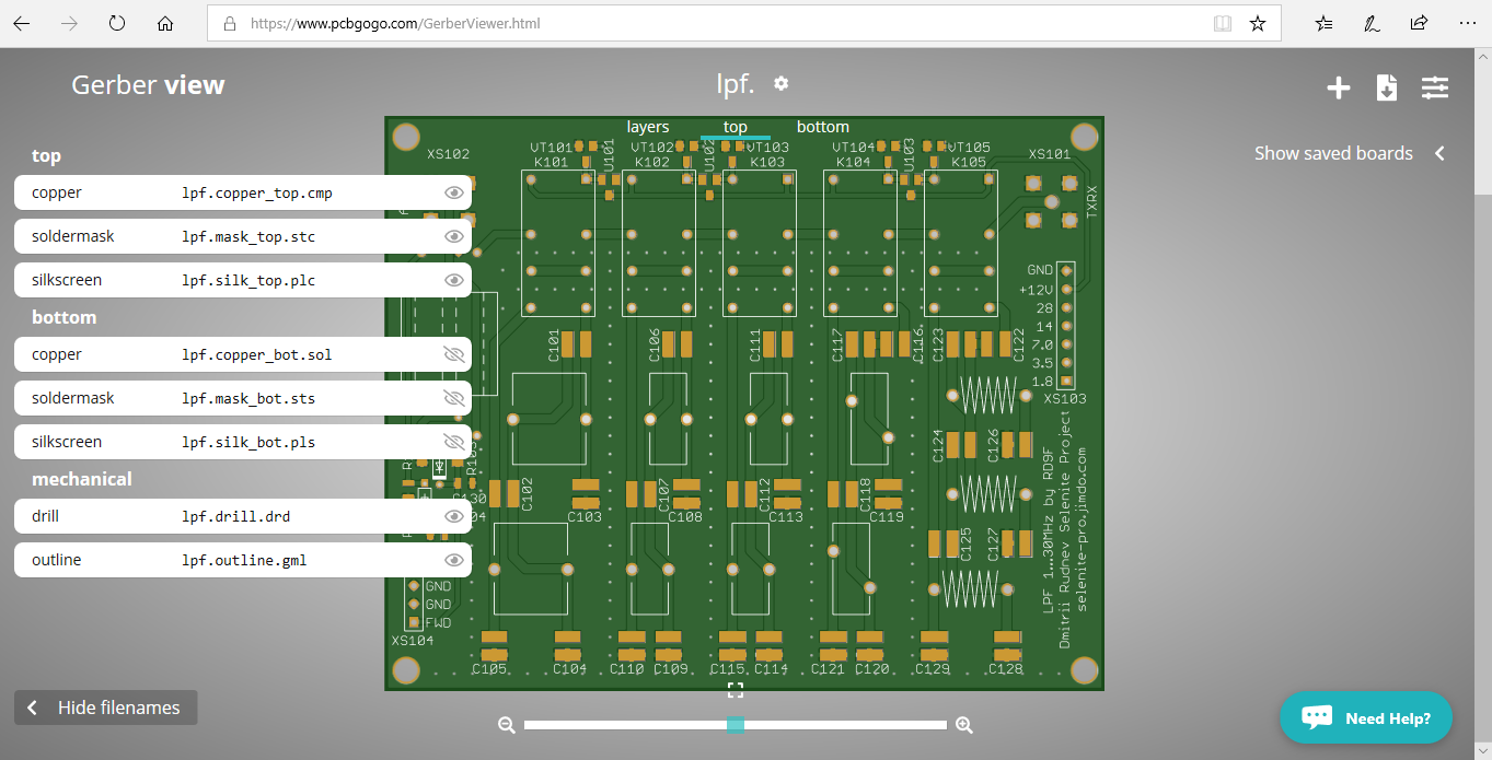
The screenshot shows the file names of the layers. Why these files have such names and extensions can be read under the "cut".
CAM processor setup
Open the project of the PCB lpf.brd from the example and through the menu File - CAM processor ... go to the processor CAM window. Open the task rs274x.cam and get:

Settings for the task tabs look like this:
| Section | Device | File name | Layer |
|---|---|---|---|
| copper_top | GERBER_RS274X | % P / RS274X /% N.copper_top.cmp | Top, Pads, Vias |
| soldermask_top | GERBER_RS274X | % P / RS274X /% N.mask_top.stc | tStop |
| silkscreen_top | GERBER_RS274X | % P / RS274X /% N.silk_top.plc | tPlace, tNames |
| copper_bottom | GERBER_RS274X | % P / RS274X /% N.copper_bot.sol | Bottom, Pads, Vias |
| soldermask_bottom | GERBER_RS274X | % P / RS274X /% N.mask_bot.sts | bStop |
| silkscreen_bottom | GERBER_RS274X | % P / RS274X /% N.silk_bot.pls | bPlace, bNames |
| drill | EXCELLON_24 | % P / RS274X /% N.drill.drd | Drills holes |
| outline | GERBER_RS274X | % P / RS274X /% N.outline.gml | Dimension |
The RS274X folder for unloading gerber files is created inside the project folder manually.
The macro% P substitutes the full path to the project folder in the name of the gerber file.
The macro% N inserts in the name of the gerber file the name of the file of the project of the circuit board from which the upload is made.
Next, the layer description that we understand is inserted into the name of the gerber file.
Gerber file extensions are selected as standard for the files of these layers in CAD Eagle 7.7.0.
The task is started using the Process_Job button. Sixteen files are uploaded to the RS274X folder, eight of which with the extensions .dpi and .dri can be safely deleted.
The remaining eight files contain data on the layers of the printed circuit board in the Gerber RS274X format and data on the holes in the Excellon format. Online Gerber Viewer on the manufacturer's website accepts these files and distributes them into layers without any additional settings.
Make sure that the gerber files are read correctly, we pack these eight files into a zip archive. This completes the project preparation of the printed circuit board for production.
And another thing: before unloading gerber files from a printed circuit board project, it does not prevent to check the compliance of this project with the manufacturer’s technological requirements.
Setting technological requirements in the project
For successful manufacturing, the design of the printed circuit board must meet the technological requirements of the manufacturer. Technological requirements in Eagle 7.7.0 contains the * .dru file attached to the PCB project.
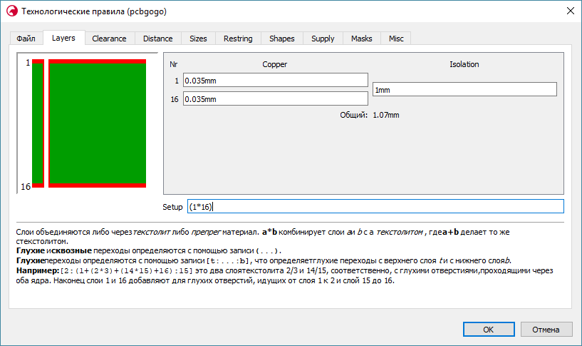
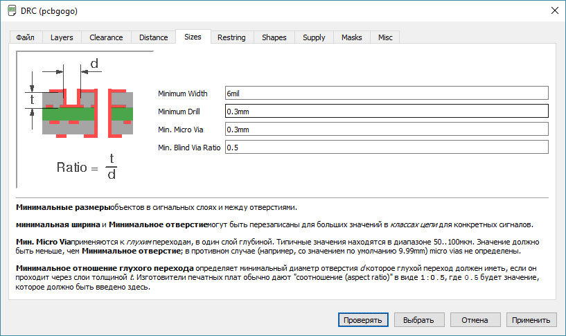
Open the PCB project lpf.brd from the example and through the Tools menu - DRC ... proceed to viewing and editing the contents of the pcbgogo.dru file:

From the unobvious : the task of a two-layer board with a thickness of 1 mm with a copper layer of 1 Oz looks like this:
From the completely unobvious : the Limit parameter sets the maximum diameter of the holes covered by the solder mask by default:
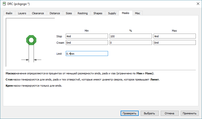
It should also be remembered that 6 mil is not exactly equal to 0.15 mm, and therefore the technological requirements of the manufacturer should be entered in the units in which they are listed on the site. For example:
What value to indicate in which parameter, on the other tabs, is clear from the prompts and data on the site’s PCB Instant Quote tab.
Tip : the pcbgogo.dru and rs274x.cam files can then be used in other projects without alterations in order to specify the technological requirements and unload the gerber files.
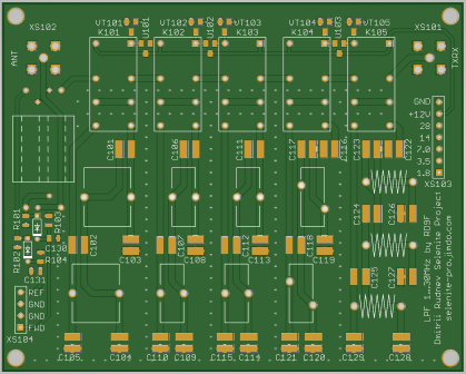
The draft low-pass filter for an amateur radio transmitter, used by the author of the publication as an example, is here .
Brief summary
This publication is analyzed on a personal example : the process of preparing a printed circuit board for production; order process for the manufacture of printed circuit boards in the PRC.
To order the manufacture of a simple prototype PCB at a Chinese factory with minimal time and money you need:
- Adjust your CAD once to the manufacturer’s technological requirements, save these technological requirements (Design Rules) to a file for future use.
- Configure once in CAD the process of unloading a printed circuit board project into Gerber RS274X + Excellon format, save the task to a file for further use.
- Before unloading the project of the printed circuit board in the gerber, it is necessary to check the project for compliance with the technological requirements of the manufacturer.
- After unloading the project of the printed circuit board in the gerber it is necessary to check the result of the unloading by the viewer.
- Place several orders with their delivery by one E-packet mail.
- Use a PayPal account to pay for the order.
I really hope that my personal experience, set forth in the publication, will help readers in organizing technical creativity. And also I really hope that any assessment of the article will be accompanied by a comment.
73! Before communication!
')
Source: https://habr.com/ru/post/450302/
All Articles