Photo excursion: what they do in the laboratory of quantum materials at ITMO University
Earlier we showed our fab lab and the laboratory of cyber-physical systems . Today you can look at the optical laboratory of the Faculty of Physics and Technology of the ITMO University.
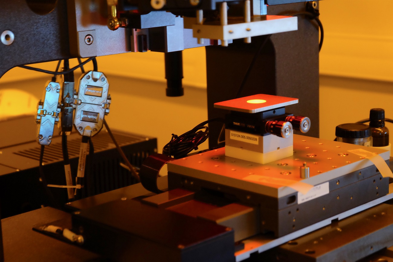
In the photo: three-dimensional nanolithograph
The laboratory of low-dimensional quantum materials belongs to the research center of nanophotonics and metamaterials ( MetaLab ) on the basis of the Faculty of Physics and Technology .
')
Its employees are studying the properties of quasiparticles : plasmons, excitons, and polaritons. These studies will make it possible to create high-grade optical and quantum computers. The laboratory is divided into several working areas covering all stages of work with low-dimensional quantum materials: sample preparation, fabrication, characterization, and optical research.
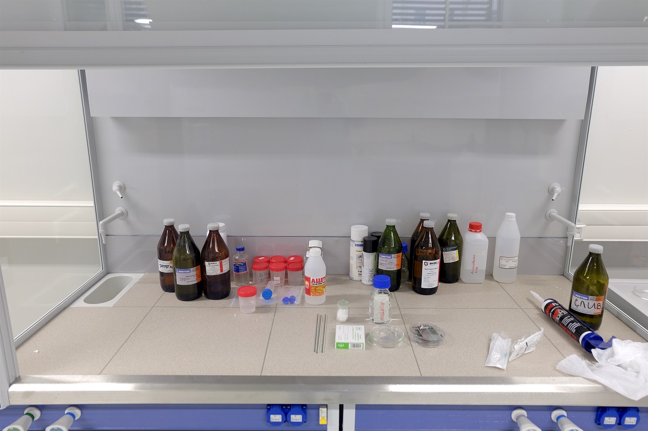
The first zone is equipped with everything necessary for the preparation of metamaterial samples.
An ultrasonic cleaner was installed to clean them, and to ensure safe handling of alcohols, a powerful extractor is equipped here. Some research materials are supplied to us by partner laboratories in Finland, Singapore and Denmark.
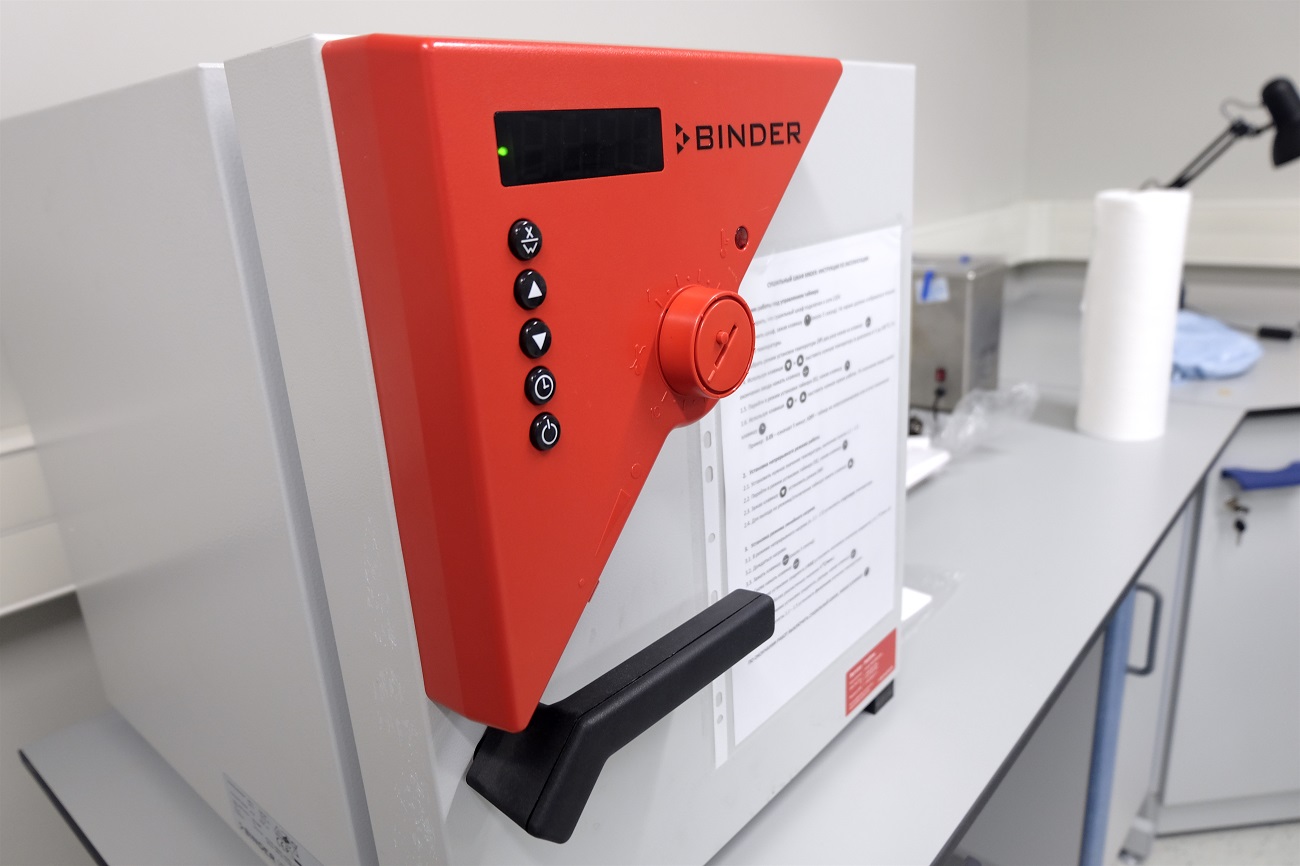
For sterilization of samples indoors there is a drying cabinet BINDER FD Classic.Line. The heating elements inside it maintain the temperature from 10 to 300 ° C. It has a USB interface for continuous temperature monitoring throughout the experiment.
Laboratory staff also use this cell to conduct stress tests and aging tests. Such experiments are necessary to understand how materials and devices behave under certain conditions: standard and extreme.
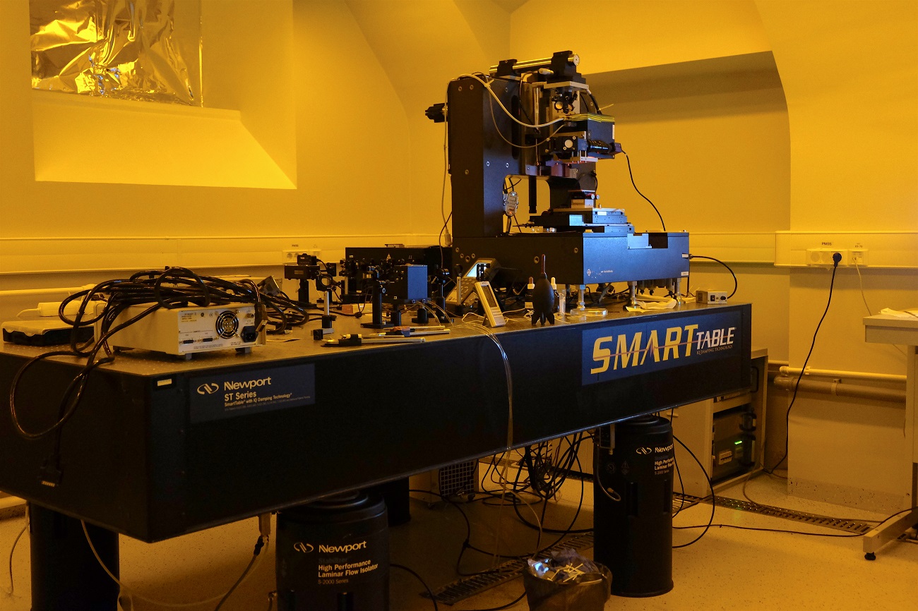
A three-dimensional nanolithograph is installed in the adjacent room. It allows fabrication of three-dimensional structures of several hundred nanometers in size.
The principle of its operation is based on the phenomenon of two-photon polymerization. In fact, it is a 3D printer that uses lasers to form an object from a liquid polymer. The polymer hardens only at the point at which the laser beam is focused.
In the photo: three-dimensional nanolithograph
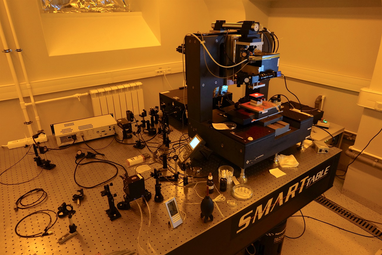
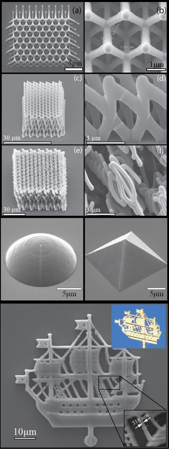
Unlike standard lithography methods, which are used to create processors and work with thin layers of materials, the two-photon polymerization method allows you to create complex three-dimensional structures. For example, these are:
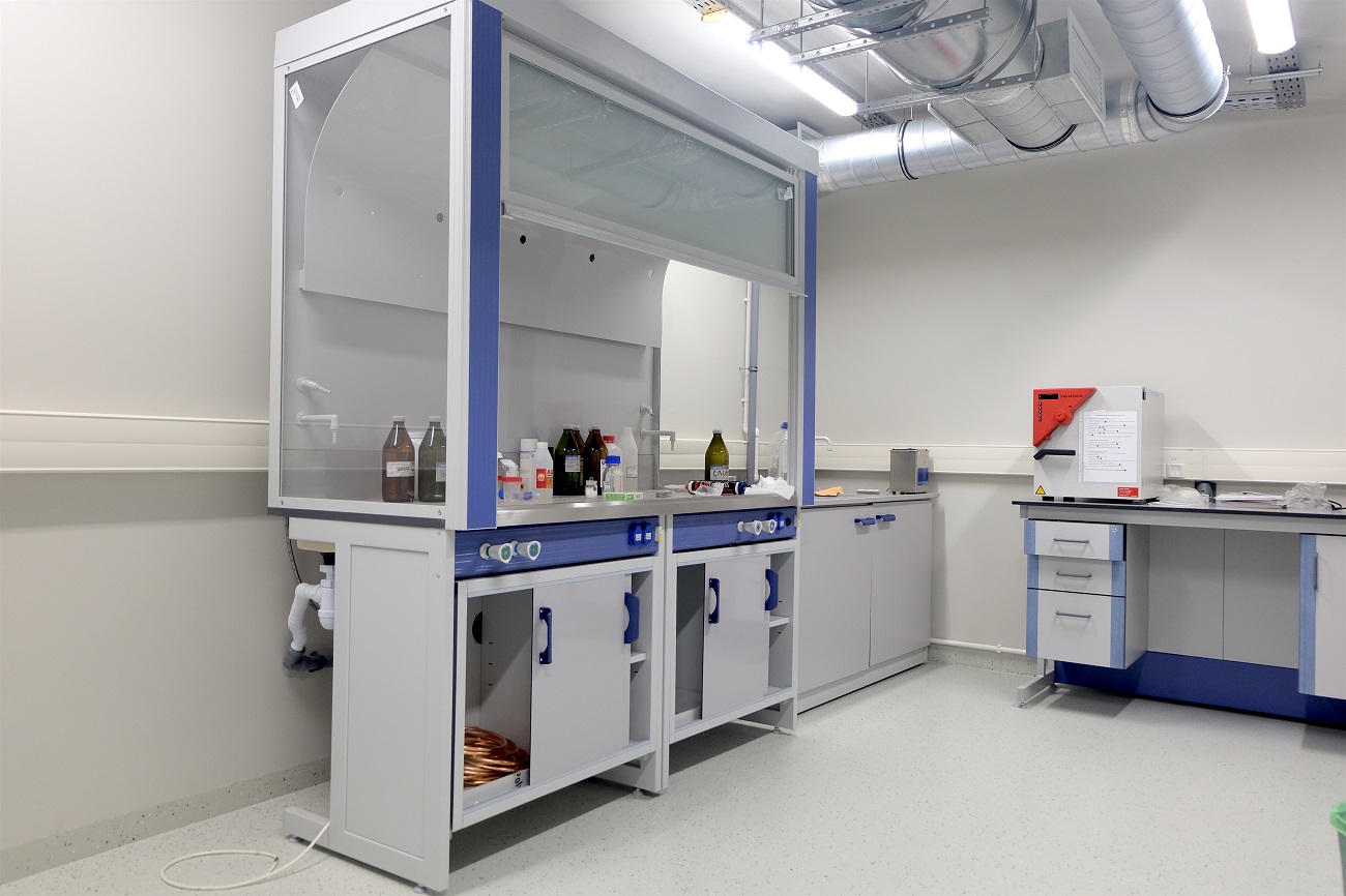
The following laboratory room is used for optical experiments.
There is a large optical table almost ten meters long, filled with numerous installations. The main elements of each installation are radiation sources (lasers and lamps), spectrometers and microscopes. One of the microscopes has three optical channels at once - upper, side and lower.
It can measure not only the transmission and reflection spectra, but also the scattering. The latter provide very rich information about nano-objects, for example, spectral characteristics and nano-antenna radiation patterns.
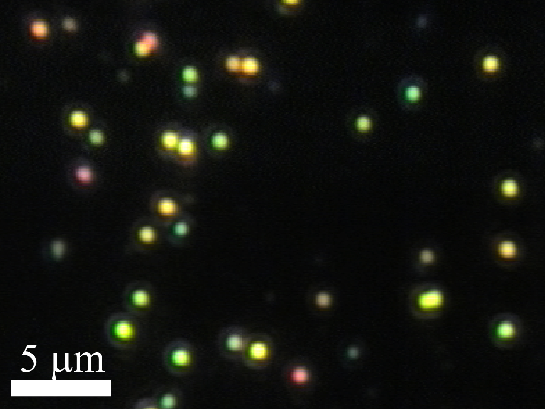
In the photo: the effect of light scattering on silicon particles
All equipment is located on the table with a single vibration reduction system. The radiation of any laser can be sent to any of the optical systems and microscopes with just a few mirrors and continue research.
A continuous-emission gas laser with a very narrow spectrum allows for Raman spectroscopy experiments. The laser beam is focused on the surface of the sample, and the spectrum of the scattered light is recorded by a spectrometer.
In the spectra, narrow lines are observed corresponding to inelastic light scattering (with a change in wavelength). These peaks provide information on the crystal structure of the sample, and sometimes even on the configuration of individual molecules.
Also installed in the room femtosecond laser. It is able to generate very short (100 femtoseconds - one ten-trillion part of a second) laser pulses with enormous power. As a result, we get the opportunity to explore nonlinear optical effects: the generation of doubled frequencies and other fundamental phenomena that are unattainable in natural conditions.

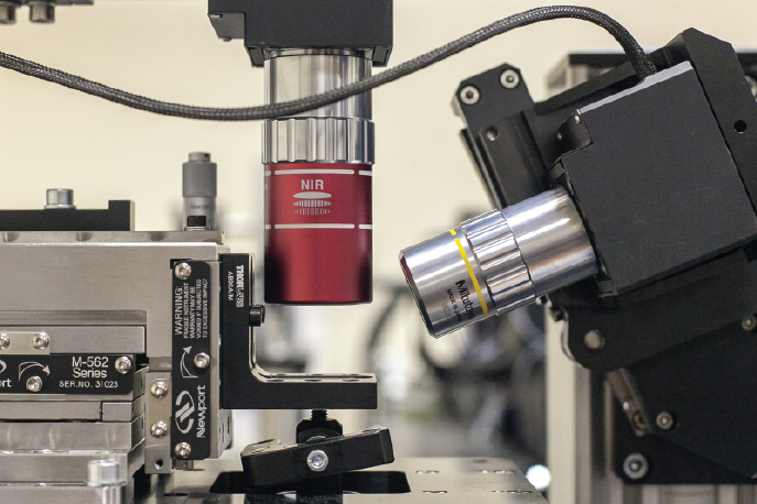
Our cryostat is also in the lab. It allows optical measurements with the same set of sources, but at low temperatures — up to seven Kelvin, which is approximately -266 ° C.
Under such conditions, a number of unique phenomena can be observed, in particular, the regime of strong coupling of light with matter, when a photon and an exciton (electron-hole pair) form a single particle — an exciton – polariton. Polaritons have great prospects in the areas of quantum computing and devices with strong non-linear effects.
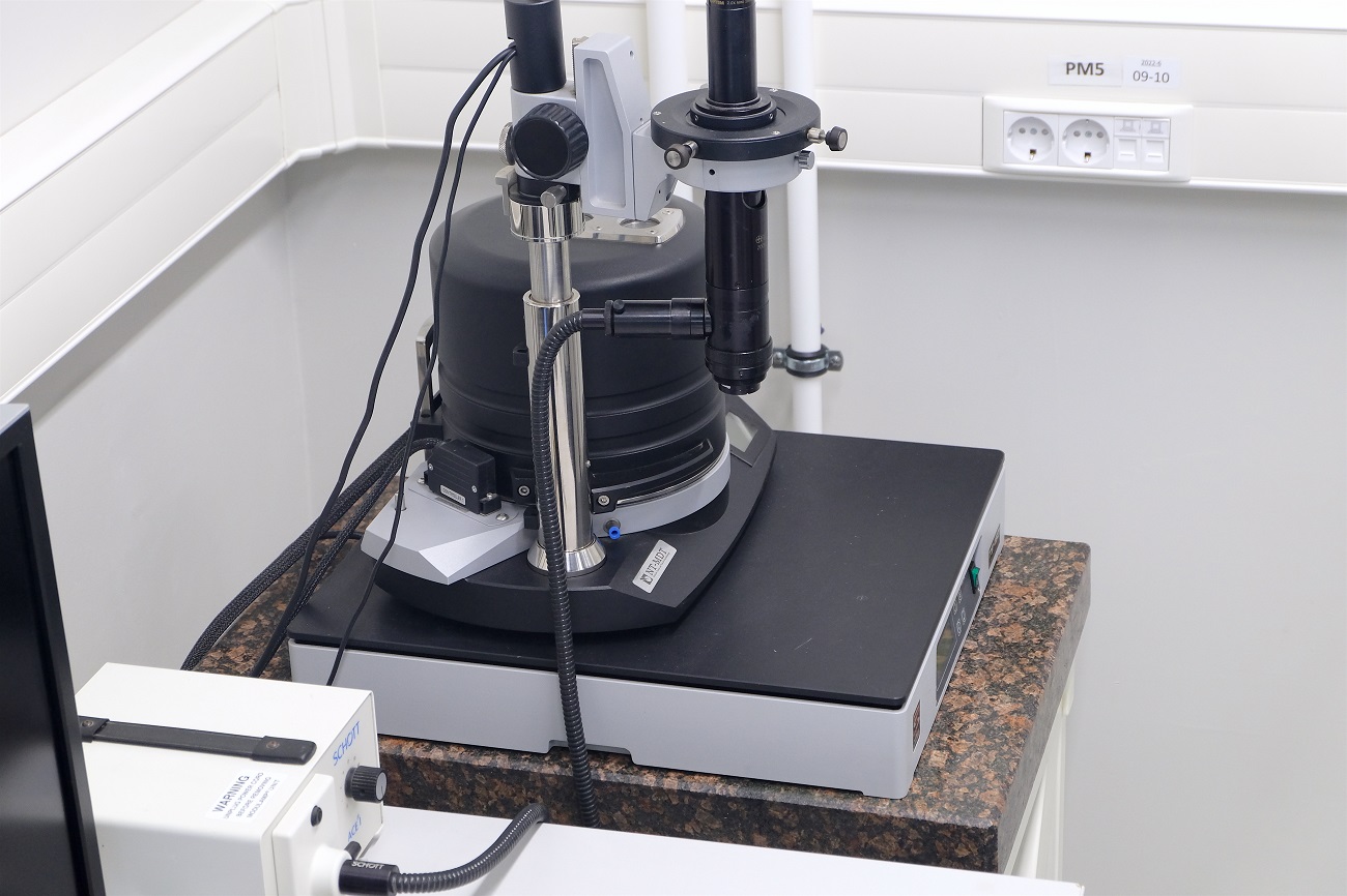
In the photo: probe microscope INTEGRA
In the last room of the laboratory, we placed our diagnostic devices - a scanning electron microscope and a scanning probe microscope . The first allows you to get an image of the surface of an object with a high spatial resolution and explore the composition, structure and other properties of the surface layers of each material. To do this, he scans them with a focused beam of electrons dispersed by high voltage.
A scanning probe microscope does the same with a probe that scans the surface of a sample. At the same time, it is possible to simultaneously obtain information on the “landscape” of the sample surface, and on its local properties, for example, electric potential and magnetization.
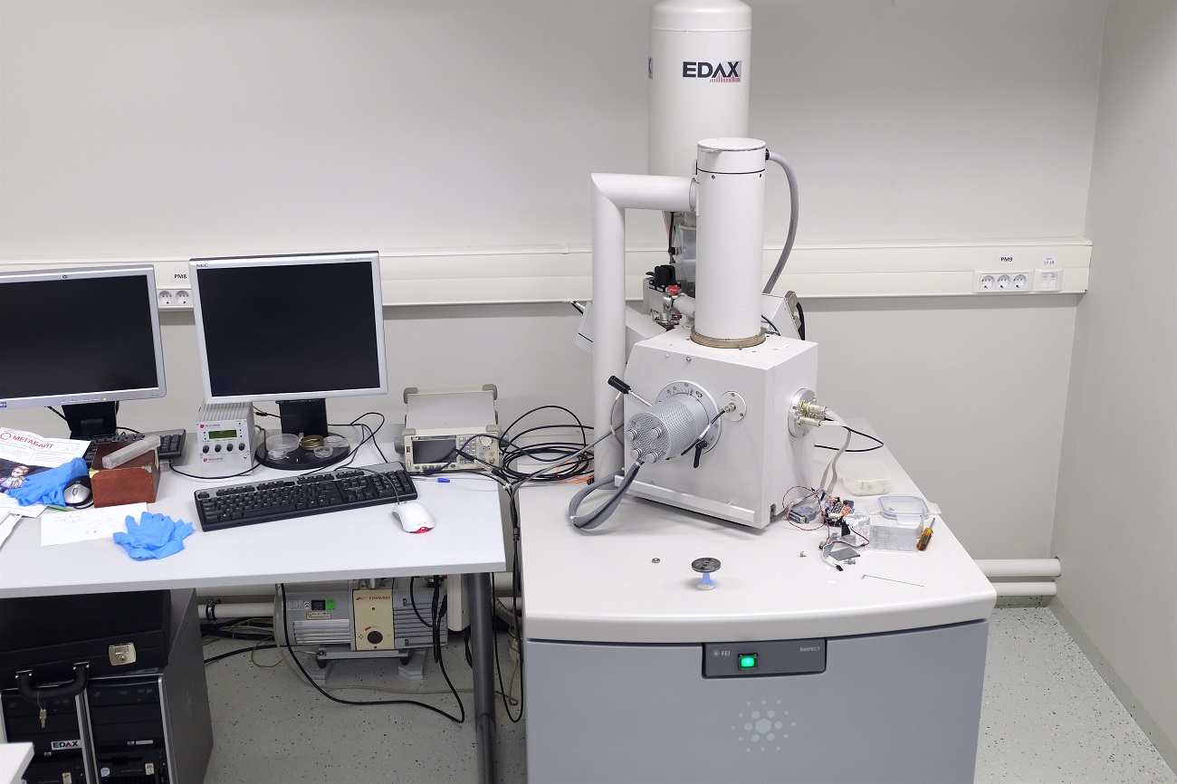
Photo: S50 scanning electron microscope (EDAX)
These instruments help us characterize samples for further optical research.
One of the main projects of the laboratory is connected with the study of hybrid states of light and matter in quantum materials - the exciton polaritons already mentioned above. This topic is devoted to the mega-grant of the Ministry of Education and Science of the Russian Federation. The project is led by a leading scientist from the University of Sheffield, Maurice Shkolnik. The experimental work on the project is conducted by Anton Samusev, and the theoretical part is headed by Professor of Physics and Technology Faculty Ivan Shelykh.
At the beginning of 2018, scientists of our University and colleagues from the university in Vladimir presented a model of a solid-state terahertz laser. The peculiarity of the development is that terahertz radiation is not “delayed” by objects made of wood, plastic and ceramics. Due to this property, the laser will be used in the areas of inspection of passengers and baggage - to quickly search for metal objects. Another area of applicability - the restoration of ancient objects of art. The optical system will help to obtain images hidden under layers of paint or ceramics.
Our plans are to equip the laboratory with new equipment in order to conduct even more complex research. For example, to purchase a tunable femtosecond laser, which will significantly expand the range of materials under study. This will help in tasks related to the development of quantum chips for next-generation computing systems.
How ITMO University works and how it lives:
In the photo: three-dimensional nanolithograph
The laboratory of low-dimensional quantum materials belongs to the research center of nanophotonics and metamaterials ( MetaLab ) on the basis of the Faculty of Physics and Technology .
')
Its employees are studying the properties of quasiparticles : plasmons, excitons, and polaritons. These studies will make it possible to create high-grade optical and quantum computers. The laboratory is divided into several working areas covering all stages of work with low-dimensional quantum materials: sample preparation, fabrication, characterization, and optical research.
The first zone is equipped with everything necessary for the preparation of metamaterial samples.
An ultrasonic cleaner was installed to clean them, and to ensure safe handling of alcohols, a powerful extractor is equipped here. Some research materials are supplied to us by partner laboratories in Finland, Singapore and Denmark.
For sterilization of samples indoors there is a drying cabinet BINDER FD Classic.Line. The heating elements inside it maintain the temperature from 10 to 300 ° C. It has a USB interface for continuous temperature monitoring throughout the experiment.
Laboratory staff also use this cell to conduct stress tests and aging tests. Such experiments are necessary to understand how materials and devices behave under certain conditions: standard and extreme.
A three-dimensional nanolithograph is installed in the adjacent room. It allows fabrication of three-dimensional structures of several hundred nanometers in size.
The principle of its operation is based on the phenomenon of two-photon polymerization. In fact, it is a 3D printer that uses lasers to form an object from a liquid polymer. The polymer hardens only at the point at which the laser beam is focused.
In the photo: three-dimensional nanolithograph
Unlike standard lithography methods, which are used to create processors and work with thin layers of materials, the two-photon polymerization method allows you to create complex three-dimensional structures. For example, these are:
The following laboratory room is used for optical experiments.
There is a large optical table almost ten meters long, filled with numerous installations. The main elements of each installation are radiation sources (lasers and lamps), spectrometers and microscopes. One of the microscopes has three optical channels at once - upper, side and lower.
It can measure not only the transmission and reflection spectra, but also the scattering. The latter provide very rich information about nano-objects, for example, spectral characteristics and nano-antenna radiation patterns.
In the photo: the effect of light scattering on silicon particles
All equipment is located on the table with a single vibration reduction system. The radiation of any laser can be sent to any of the optical systems and microscopes with just a few mirrors and continue research.
A continuous-emission gas laser with a very narrow spectrum allows for Raman spectroscopy experiments. The laser beam is focused on the surface of the sample, and the spectrum of the scattered light is recorded by a spectrometer.
In the spectra, narrow lines are observed corresponding to inelastic light scattering (with a change in wavelength). These peaks provide information on the crystal structure of the sample, and sometimes even on the configuration of individual molecules.
Also installed in the room femtosecond laser. It is able to generate very short (100 femtoseconds - one ten-trillion part of a second) laser pulses with enormous power. As a result, we get the opportunity to explore nonlinear optical effects: the generation of doubled frequencies and other fundamental phenomena that are unattainable in natural conditions.
Our cryostat is also in the lab. It allows optical measurements with the same set of sources, but at low temperatures — up to seven Kelvin, which is approximately -266 ° C.
Under such conditions, a number of unique phenomena can be observed, in particular, the regime of strong coupling of light with matter, when a photon and an exciton (electron-hole pair) form a single particle — an exciton – polariton. Polaritons have great prospects in the areas of quantum computing and devices with strong non-linear effects.
In the photo: probe microscope INTEGRA
In the last room of the laboratory, we placed our diagnostic devices - a scanning electron microscope and a scanning probe microscope . The first allows you to get an image of the surface of an object with a high spatial resolution and explore the composition, structure and other properties of the surface layers of each material. To do this, he scans them with a focused beam of electrons dispersed by high voltage.
A scanning probe microscope does the same with a probe that scans the surface of a sample. At the same time, it is possible to simultaneously obtain information on the “landscape” of the sample surface, and on its local properties, for example, electric potential and magnetization.
Photo: S50 scanning electron microscope (EDAX)
These instruments help us characterize samples for further optical research.
Projects and Plans
One of the main projects of the laboratory is connected with the study of hybrid states of light and matter in quantum materials - the exciton polaritons already mentioned above. This topic is devoted to the mega-grant of the Ministry of Education and Science of the Russian Federation. The project is led by a leading scientist from the University of Sheffield, Maurice Shkolnik. The experimental work on the project is conducted by Anton Samusev, and the theoretical part is headed by Professor of Physics and Technology Faculty Ivan Shelykh.
Also, laboratory staff are studying ways to transfer information using solitons. Solitons are waves that are not affected by dispersion. Due to this, the signals transmitted by solitons do not “spread out” as they propagate, which makes it possible to increase both the speed and the transmission distance.
At the beginning of 2018, scientists of our University and colleagues from the university in Vladimir presented a model of a solid-state terahertz laser. The peculiarity of the development is that terahertz radiation is not “delayed” by objects made of wood, plastic and ceramics. Due to this property, the laser will be used in the areas of inspection of passengers and baggage - to quickly search for metal objects. Another area of applicability - the restoration of ancient objects of art. The optical system will help to obtain images hidden under layers of paint or ceramics.
Our plans are to equip the laboratory with new equipment in order to conduct even more complex research. For example, to purchase a tunable femtosecond laser, which will significantly expand the range of materials under study. This will help in tasks related to the development of quantum chips for next-generation computing systems.
How ITMO University works and how it lives:
Source: https://habr.com/ru/post/449778/
All Articles