The history of the transistor, part 3: multiple reinvention
Other articles of the cycle:
- Relay history
- The history of electronic computers
- Transistor history
For more than a hundred years, the analog dog wagged a digital tail. Attempts to expand the capabilities of our senses - sight, hearing, and even, in a sense, touch, led engineers and scientists to search for the best components for telegraph, telephone, radio and radar. It was only by luck that these searches found a way to create new types of digital machines. And I decided to tell the story of this constant exportation , during which telecommunication engineers supplied raw materials for the first digital computers, and sometimes even designed and built these computers themselves.
')
But by the 1960s, this fruitful collaboration had come to an end, and with it my story. Digital equipment manufacturers no longer needed to look into the world of telegraph, telephone, and radio in search of new, improved switches, since the transistor itself provided an inexhaustible source of improvements. Year after year, they dug deeper and deeper, always finding ways to exponentially increase work speed and reduce cost.
However, none of this would have happened if the invention of the transistor had stopped at the work of Bardeen and Brettein .
Slow start
In the popular press, there was no active enthusiasm for the announcement of Bell's laboratories about the invention of the transistor. July 1, 1948 in the New York Times, this event was given three paragraphs at the bottom of the News Radio. Moreover, this news appeared after others, obviously, who were considered more important: for example, the time show “Waltz Time”, which was supposed to appear on NBC. With hindsight, we may want to laugh, or even scolding unknown authors - how could they not recognize the event that had turned the world around?

But a look into the past distorts perception, amplifying those signals whose significance we know, although at that time they were lost in a sea of noise. The 1948 transistor was very different from computer transistors, on one of which you read this article (unless you decide to print it out). They differed so much that, despite the same name, and the continuous line of inheritance linking them, they should be considered as different types, if not different genera. They have different compositions, a different structure, a different principle of functioning, not to mention a gigantic difference in size. Only thanks to the constant re-inventions did the clumsy device built by Bardin and Brettein transform the world and our lives.
In fact, a germanium transistor with a single point of contact did not deserve more attention than it had received. He had several defects inherited from the electron tube. He, of course, was much smaller than the most compact lamps. The absence of a hot thread meant that it produces less heat, consumes less energy, does not burn out and does not require warming up before use.
However, the accumulation of dirt on the contact surface led to failures and negated the potential for a longer service life; he gave a louder signal; worked only at low power and in a narrow frequency range; refused in the presence of heat, cold or humidity; and it could not produce uniformly. Several transistors created by the same people in the same way would have defiantly different electrical characteristics. And all this was accompanied by the cost of eight times greater than that of a standard lamp.
It was not until 1952 that Bell Laboratories (and other patent holders) solved manufacturing problems enough for one-point transistors to become practical devices, and even then they didn’t particularly spread beyond the hearing aid market, where price sensitivity was relatively low, and the benefits of battery life outweigh the drawbacks.
However, the first attempts to turn the transistor into something better and more useful had already begun. They actually began much earlier than the moment when the public learned about its existence.
Ambitions Shockley
By the end of 1947, Bill Shockley, in great excitement, made the trip to Chicago. He had vague ideas about how to transcend the transistor recently invented by Bardin and Brettein, but he has not yet had a chance to develop them. Therefore, instead of enjoying the break between the stages in his work, he spent Christmas and New Year at the hotel, filling out about 20 pages of notebook with his ideas. Among them was the proposal of a new transistor consisting of a semiconductor sandwich - a slice of p-type germanium between two pieces of n-type.
Encouraged by the presence of such an ace in the sleeve, Shockley made claims to Bardin and Brettein for their return to Murray Hill, demanding all the glory for inventing the transistor. Did not his idea of the field effect make Bardin and Brettein sit down in the lab? Isn’t it necessary because of this to transfer all rights to a patent to him? However, Shockley’s cunning went sideways: Bella’s patent lawyers found out that an unknown inventor, Julius Edgar Lilienfeld , patented a field effect semiconductor amplifier almost 20 years before, in 1930. Lilienfeld, of course, did not embody his idea, given the state materials at that time, but the risk of crossing was too great - it was better to completely avoid mentioning the field effect in the patent.
So, although Bell’s laboratories gave Shockley a generous share of the inventor’s fame, they only mentioned Bardeen and Brettein in the patent. However, you cannot bring back what has been done: Shockley's ambitions have destroyed his relationship with two subordinates. Bardeen stopped working on the transistor, and concentrated on superconductivity. He left the laboratories in 1951. Brettein stayed there, but refused to work with Shockley again, and insisted on transferring to another group.
Because of his inability to work with other people, Shockley did not progress in the laboratories, so he also left there. In 1956, he returned home to Palo Alto to establish his own transistor manufacturing company, Shockley Semiconductor. Before leaving, he broke up with his wife, Gene, when she was recovering from uterine cancer, and met Emmy Lenning, whom she soon married. But of the two halves of his California dream — the new company and the new wife — only one was fulfilled. In 1957, his best engineers, enraged by his management style and the direction in which he led the company, left him to establish a new firm, Fairchild Semiconductor.
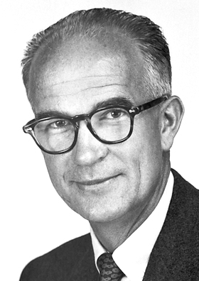
Shockley in 1956
So Shockley threw the empty shell of his company and got a job at the electrical engineering department at Stanford. There, he continued to push his colleagues (and his oldest friend, physicist Fred Seitz ) away from him with the theories of racial degeneration and racial hygiene that interested him — themes that were unpopular in the United States since the end of the last war, especially in academia. He found pleasure in unleashing disputes, inflating the media and provoking protests. He died in 1989, estranged from his children and colleagues, and was only visited by his second wife, Amy, who was forever devoted to him.
Although his miserable attempts in the field of entrepreneurship failed, Shockley dropped the grain into the fertile soil. The San Francisco Bay Area produced a multitude of small electronics companies that were flavored by the federal government during the war. Fairchild Semiconductor, Shockley's random scion, spawned dozens of new companies, a couple of which are still known today: Intel and Advanced Micro Devices (AMD). By the early 1970s, this area has earned the mocking nickname "Silicon Valley". But wait a minute - after all, Bardeen and Brettein created a germanium transistor. Where did the silicon come from?

So in 2009, it looked like an abandoned place in Mountain View, where Shockley Semiconductor was previously located. Today the building is demolished.
To silicon intersection
The fate of a new type of transistor, invented by Shockley in a Chicago hotel, was much happier than that of its inventor. All thanks to the desire of one person to grow uniform pure semiconductor crystals. Gordon Thiel, a physical chemist from Texas who studied germanium, which was then useless then for his doctoral thesis, got a job in the Bell laboratory in the 1930s. After learning about the transistor, he was convinced that its reliability and power can be significantly improved by creating it from a pure single crystal, and not from the then used polycrystalline mixtures. Shockley rejected his attempts, considering them a waste of resources.
However, Thiel persisted and succeeded, with the help of mechanical engineer John Little, creating a device that reaches a tiny germ of a crystal from molten germanium. Cooled around the embryo, germanium expanded its crystal structure, creating a continuous and almost pure semiconducting lattice. By the spring of 1949, Til and Little could create crystals on order, and tests showed that they left far behind their polycrystalline competitors. In particular, nonbasic carriers added to them could survive within a hundred microseconds or even longer (against no more than ten microseconds in other crystal samples).
Now Thiel could afford more resources, and he recruited more people to his team, among whom was another physical chemist who came to Bell's lab in Texas - Morgan Sparks. They began to change the melt for the manufacture of germanium p-type or n-type, adding balls of the corresponding impurities. For another year they improved the technology to such an extent that they could grow a germanium npn sandwich directly in the melt. And it worked exactly as Shockley predicted: an electrical signal of a p-type material modulated an electrical current between two conductors connected to its n-type pieces.
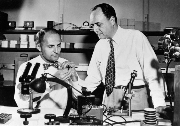
Morgan Sparks and Gordon Teale at the Bench in Bella's Labs
This transistor with a grown transition surpassed its ancestor with a single point contact in almost all respects. In particular, it became more reliable and predictable, produced much less noise (and, therefore, was more sensitive), and extremely energy-efficient - consuming a million times less energy than a typical electronic lamp. In July 1951, Bell Laboratories organized another press conference to announce the new invention. Even before the first transistor managed to enter the market, it, in fact, had already become insignificant.
And yet it was only the beginning. In 1952, General Electric (GE) announced the development of a new process for creating transistors with a transition, a fused method. Within its framework, two indium pellets (p-type donor) were fused on both sides of a thin slice of n-type germanium. This process was simpler and cheaper than growing transitions in the alloy, such a transistor gave less resistance and supported high frequencies.
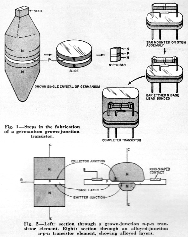
Grown and Alloy Transistors
The following year, Gordon Teale decided to return to his home state, and got a job at Texas Instruments (TI) in Dallas. The company was founded under the name of Geophysical Services, Inc., and first produced equipment for the exploration of oil fields, TI opened the electronics division during the war, and now entered the transistor market under license from Western Electric (Bella Laboratories production division).
Teal brought with him new skills learned in laboratories: the ability to grow and alloy single-crystal silicon. The most obvious weakness of germanium was its sensitivity to temperature. Being exposed to heat, the atoms of germanium in a crystal quickly dumped free electrons, and it became more and more a conductor. At a temperature of 77 ° C, he stopped working altogether, like a transistor. The main goal of transistor sales was the armed forces - a potential consumer with low price sensitivity and a huge need for stable, reliable and compact electronic components. However, temperature-sensitive germanium would not be useful in many cases of military use, especially in the aerospace field.
Silicon was much more stable, but it had to pay a much higher melting point, comparable to that of steel. This caused enormous difficulties, given that very clean crystals were required to create high-quality transistors. Hot melted silicon would absorb contaminants from any crucible it was in. Teal and the team from TI were able to overcome these difficulties with the help of ultra-pure silicon samples from DuPont. In May 1954, at the conference of the Institute of Radio Engineers in Dayton (Ohio), Thiel demonstrated that the new silicon devices manufactured in his laboratory continued to work, even while being immersed in hot oil.
Successful upstarts
Finally, about seven years after the first invention of the transistor, it could be made from the material with which it became synonymous. And about the same time will pass before the appearance of transistors, roughly resembling the form used in our microprocessors and memory chips.
In 1955, scientists from Bell's laboratories successfully learned how to make silicon transistors with a new doping technology - instead of adding solid balls of impurities to a liquid melt, they introduced gaseous additives into the solid surface of a semiconductor ( thermal diffusion ). Carefully controlling the temperature, pressure and duration of the procedure, they reached exactly the required depth and degree of doping. Strengthening the control over the production process gave increased control over the electrical properties of the final product. What else is important, thermal diffusion made it possible to produce a product in batches - it was possible to dope a large silicon slab, and then cut it into transistors. The military provided funding for Bell’s laboratories, since the organization of production required high upfront costs. They needed a new product for an ultrahigh-frequency early radar detection line (" Dew line "), a chain of arctic radar stations designed to detect Soviet bombers flying from the North Pole, and they were ready to pay $ 100 per transistor (these were times when the the car could be bought for $ 2000).
Doping together with photolithography , which controlled the location of impurities, made it possible to etch the entire circuit on a single semiconductor substrate — before that, they simultaneously thought of Fairchild Semiconductor and Texas Instruments in 1959. Planar technology from Fairchild used chemical deposition of metal films connecting the electrical transistors of the transistor. It eliminated the need for manual wiring, reduced production costs, and increased reliability.
Finally, in 1960, two engineers from Bell Laboratories (John Atalla and Devon Kahn) implemented the original Shockley concept of a field effect transistor. A thin oxide layer on the semiconductor surface was able to effectively suppress surface states, as a result of which the electric field from the aluminum gate penetrated into the silicon. So was born the MOSFET [metal-oxide semiconductor field-effect transistor] (or MOS-structure, from metal-oxide-semiconductor), which turned out to be so easy to miniaturize, and which is still used in almost all modern computers (interestingly, Atallah was come from Egypt, and Kahn from South Korea, and practically only these two engineers from our entire history have no European roots).
Finally, thirteen years after the invention of the first transistor, something resembling the transistor of your computer appeared. It was easier to produce, he used less energy than a junction transistor, but he rather slowly responded to the signals. Only after the proliferation of large-scale integrated circuits with hundreds or thousands of components located on a single chip, the advantages of field-effect transistors came to the fore.

Illustration of a patent field-effect transistor
The field effect was Bell’s laboratories ’latest serious contribution to the design of the transistor. Major electronics manufacturers such as Bell Laboratories (with their Western Electric), General Electric, Sylvania and Westinghouse have built up an impressive amount of semiconductor research. From 1952 to 1965, Bell's laboratories alone registered more than two hundred patents on this topic. Still, the commercial market quickly passed into the hands of such new players as Texas Instruments, Transitron and Fairchild.
The early transistor market was too small for big players to pay attention to: about $ 18 million a year in the mid-1950s, compared with a total of $ 2 billion in the electronics market. However, the research laboratories of these giants served as unintended training camps, where young scientists could absorb the knowledge concerning semiconductors, so that later they could start selling their services to smaller firms. When the market for tube electronics in the mid-1960s began to squeeze seriously, for Bell laboratories, Westinghouse and the rest it was already too late to compete with upstarts.
Transition of computers to transistors
In the 1950s, transistors invaded the world of electronics in four of the most significant areas. The first two were hearing aids and portable radios, in which low power consumption and, as a result, long battery life, overpowered other considerations. The third was military use. The US Army had high hopes for transistors as reliable and compact components that can be used anywhere, from field radio to ballistic missiles. However, at first, their spending on transistors was more like a bet on the future of technology than on confirming their value at that time. And finally, there was still digital computing.
In the computer field, the shortcomings of the switches on electronic tubes were well known, and some skeptics even considered before the war that an electronic computer could not be made practical. When thousands of lamps were collected in one device, they devoured electricity, producing a huge amount of heat, and in terms of reliability, you could only rely on their regular burnout. Therefore, a low-power, cold, and filament-free transistor became the savior of computer manufacturers. Its disadvantages as an amplifier (for example, a louder output signal) did not present such a problem when used as a switch. The only obstacle was the cost, and at one time it would begin to fall sharply.
All early American experiments with transistor computers took place at the intersection of the military's desire to explore the potential of a promising new technology, and the desire of engineers to switch to improved switches.
In 1954, Bell’s laboratories built the TRADIC for the United States Air Force to see if the transistors would be able to install a digital computer on board a bomber, replacing it with analog navigation and help finding targets. The MIT Lincoln Laboratory developed the TX-0 computer as part of an extensive air defense project in 1956. The machine used another transistor variant, a surface barrier, well suited for high-speed computations. Philco built its computer SOLO under a contract with the Navy (but really - at the request of the NSA), ending it in 1958 (using another version of the surface-barrier transistor).
In Western Europe, not so resourced during the Cold War, the story was very different. Machines such as Manchester Transistor Computer, Harwell CADET (another name inspired by the ENIAC project, and encrypted with writing backwards), and the Austrian Mailüfterl were side projects that used the resources that their creators could scrape together - including transistors with one first-generation contact point .
There is a lot of controversy over the title of the first computer using transistors. All, of course, rests on the choice of the correct definitions of such words as "first", "transistor" and "computer". In any case, we know where the story ends. Commercialization of transistor computers began almost immediately. Year after year, computers for the same price became more powerful, and computers of the same power became cheaper, and this process seemed so inexorable that it was elevated to the rank of law, alongside gravity and energy conservation. Do we need to argue about which stone was the first in the fall?
Where did Moore's law come from?
Approaching the end of the switch history, it is worth asking the question: what led to the appearance of this collapse? Why does Moore's law exist (or existed — let us argue about this another time)? For airplanes or vacuum cleaners Moore's law is not, as there is no it for electronic lamps or relays.
The answer consists of two parts:
- The logical properties of the switch as an artifact category.
- The ability to use purely chemical processes for the manufacture of transistors.
First, the essence of the switch. The properties of most artifacts must satisfy a wide range of inexorable physical limitations. Passenger aircraft must withstand the total weight of many people.The vacuum cleaner should be able to suck a certain amount of dirt for a certain time from a certain physical area. Planes and vacuum cleaners will be useless if reduced to nanoscale.
At the same switch - an automatic switch, which has never been touched by a human hand - physical limitations are much less. He must have two different states, and he must be able to tell other similar switches to change their states. That is, all he has to be able to do is turn on and off. What is so special about transistors? Why haven't other types of digital switches experienced such exponential improvements?
Here we come to the second fact. Transistors can be manufactured using chemical processes without mechanical intervention. From the very beginning, the key element in the production of transistors was the use of chemical impurities. Then a planar process appeared, eliminating the last mechanical step from production - the connection of wires. As a result, he got rid of the last physical constraint on miniaturization. Transistors no longer needed to be large enough for a person’s fingers — or for any mechanical device. Everything was done by simple chemistry, on an unimaginably small scale: acid for etching, light to control which parts of the surface will resist etching, and vapors for introducing impurities and metal films onto etched tracks.
Why do we need miniaturization? Reducing the size gave a whole galaxy of pleasant side effects: an increase in switching speed, a decrease in energy consumption and the cost of individual specimens. These powerful incentives led everyone to look for ways to further reduce the switches. And the semiconductor industry for the life of one person has passed from the manufacture of switches the size of a nail to the packaging of tens of millions of switches per square millimeter. From a request of eight dollars for one switch to a proposal of twenty million switches for a dollar.
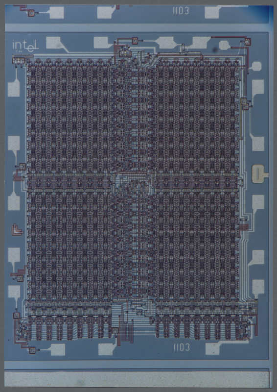
Intel 1103 memory chip from 1971. Individual transistors, measuring only tens of micrometers, are already indistinguishable by the eye. And since then they have decreased a thousand times.
What else to read:
- Ernest Bruan and Stuart MacDonald, Revolution in Miniature (1978)
- Michael Riordan and Lillian Hoddeson, Crystal Fire (1997)
- Joel Shurkin, Broken Genius (1997)
Source: https://habr.com/ru/post/449760/
All Articles