Computer architecture. Digital logic level
A computer is a machine that can perform calculations through the execution of primitive operations. It can understand only two signals, which are taken as 0 and 1.
The organization of the architecture of machines is represented as a series of levels, each of which is built on above the underlying level. This is done for a reason, with the help of a multi-tier architecture, we can abstract from the implementation and complexity of the lower level, thereby facilitating the design process and reducing the likelihood of errors. Abstraction is a key point in the entire computer architecture.
Computer organization consists of 6 levels: digital logic, microarchitecture, instruction set architecture (ISA), operating system, assembly language, applied, of course, except for the physical layer, which is below the digital logic level. I do not yet have plans to tell everything that happens above the level of ISA. There are two reasons for this: firstly, the purpose of these articles is not to consider all levels, but to show what levels 0-2 are, and, secondly, there is on habr'e Many articles on the levels above ISA and without me. This article will show the digital logic level, and in the next two microarchitecture and instruction set architecture, respectively.
Digital logic level is essentially a set of logical functions that interact with each other to perform a larger task. All work at this level consists of two basic concepts: gates and Boolean algebra . First, I will talk about them, and then about the logic circuits and how they are used in the development, and finally, what the memory is and how it is implemented.
')
The gate (Fig. 1.0) is a device that receives input signals and provides output, it is implemented on transistors (I will not talk about their work). Gates are used at this level as a “building” material to represent basic logical operations, and then they are combined to implement certain schemes, that is, the meaning of this level is to build reusable circuits, and not about the operation of gates (and transistors) ; Further, on the basis of these schemes, more complex and highly specialized schemes can be built, for example, whole memory modules, different logic, for example, in order for CPU components to interact at the microarchitecture level, etc.
Figure 1.0. The image of the valves.

Table 1.0. Truth table for basic operations.
This type of algebra works with 0 and 1, there are such operations (Table 1.0) as: AND (conjunction), OR (disjunction), NOT (denial), EXCLUSIVE OR, and their combinations, etc. You can use different methods to describe logical functions, but we will concentrate on only two: the truth table and the disjunctively normal form.
To build a truth table, we simply iterate over all combinations of the values of all variables. The table allows us to see all possible combinations in which the function takes the values of truth or false, it is suitable when we need such a property, for example, a decoder. The disjunctively normal form allows us to reduce its table size; for this, we use only those combinations of variable values for which the function takes only true values. To create a scheme that will take the true value only with the necessary combinations, we need to present these lines as minters .
Minterma is a logical function that takes a true value only with one set of values of variables included in it, it is realized by taking AND from all variables (with or without NOT). For example! A & B & C (! - NOT, & - AND) takes the true value only when A = 0, B = C = 1. When we present all true strings in the form of minters, we need to take from all the minters OR (disjunction). So now, combining all the above, we can implement the function in the form of a diagram.
For example, let's take the EXCLUSIVE OR function (Table 1.0). We see that it has two true lines: with A = 0, B = 1 and A = 1, B = 0. We take and present them as two mintherms,! A & B and A &! B. Indeed, the first minterma is equal to 1 only in the case when A = 0, B = 1; Another only in the case when A = 1, B = 0; Just the same with us, only such rows in the truth table take true values. Now that we have all the necessary mintermas, we take the OR operation from all the minters, that is, (A &! B) | (! A & B). We took and presented the function EXCLUSIVE OR in the form of a formula, which we can easily represent in the form of a logical scheme (Figure 1.1a), because it consists of simple functions: two AND and one OR. It would be more efficient if we reduced the number of inputs (Fig. 1.1b), for this you can combine A with! A into one input A, you only need to add another gate between the new input A and the old input! A NOT to allow the input signal for A was the opposite for old A and! A; We can do the same with B and! B.
Figure 1.1. An EXCLUSIVE OR Schema (the bar above the variable denotes NOT).

A logic circuit is a set of integrated valves with input and output signals. Figure 1.1 also shows a circuit in which the input signals are A and B, the output signal comes from the OR operation; it also has three valves: two AND, one OR. Now let's look at some types of schemes with which we need to meet in the future, these include: combinational, arithmetic, integrated circuits.
A combination circuit is a circuit with one additional property: the values of the output signals depend only on the input, or in other words, there are no storage devices in it. Reusable components are created from this kind of circuits, which are used to implement most other circuits. We will consider several, namely: comparator, decoder, multiplexer / demultiplexer.
Comparator
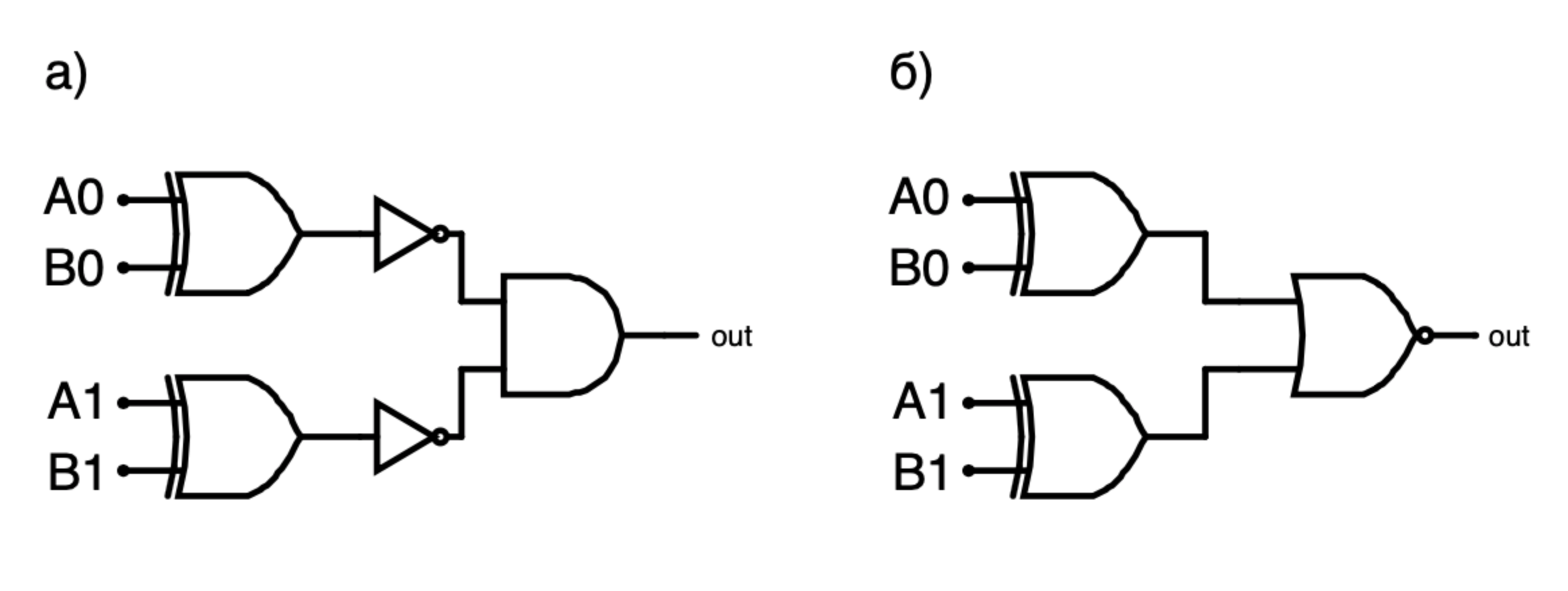
A comparator has n input paired lines (i.e., 2n inputs) and one output line. The logic of his work is to compare each pair of bits (bits of the word A are compared with the corresponding bits of the word B) and, if one of them is unequal, return 0 (if 0 is false), otherwise 1. Let's build a truth table (Table. 1.1) for one-bit comparator; you can see that it is equal to the truth table EXCLUSIVE OR NOT (when NOT is added to the operation, then all output values in the table become opposite). Now let's expand it to a two-bit comparator, construct a truth table (Table 1.2) for it from two variable values of which depend on two single-bit comparators, that is, on two EXCLUSIVE OR NONE; in it, the value 1 in CMP0 (and CMP1) means that two inputs of a comparator are equal, 0 is vice versa, that is, 1 in the R column should be only when the values are equal in two comparators. This truth table coincides with the AND table, that is, we combine all the EXCLUSIVE OR NOT operation AND and we get a two-bit comparator (Fig. 1.3a). For further expansion of the comparator, it is only necessary to add EXCLUSIVE OR-NOT and connect it to I. The disadvantage of such an implementation is its redundancy, we need to add valves NOT for each EXCLUSIVE OR; we can get rid of this (Fig. 1.3b) if we replace the AND gate with NOT the inputs to OR-NOT, since their truth tables are the same.
Table. 1.1. Truth table for one-bit comparator.
Table. 1.2. Truth table for two-bit comparator.
Figure 1.3. Two schemes of two-bit comparators.
Decoder
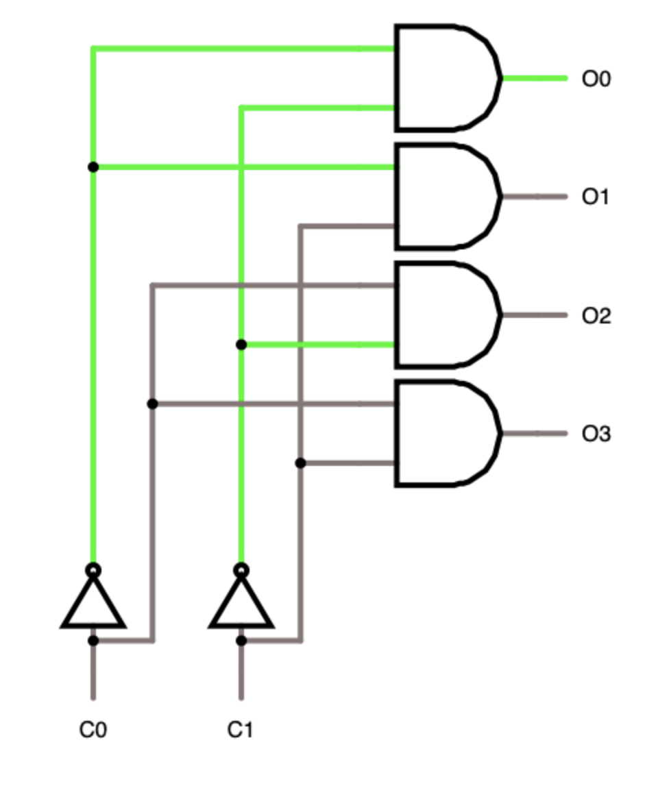
The decoder has n input lines, 2 ^ n output, it is implemented so that the signal (true, 1) passes only to one output line. Each output gate AND receives its own combination of variable values that (values) are in some row of the truth table, and as we already know, the row of the truth table can be implemented as a minter, that is, we represent each row as the AND gate (Fig. 1.4 ) from several variables. The main use of a decoder is to selectively include different parts of a circuit (or circuits), for example, the ALU (about it later) has several operations that it can perform on input values to select one of them using a decoder.
Figure 1.4 Decoder.
Multiplexer / Demultiplexer
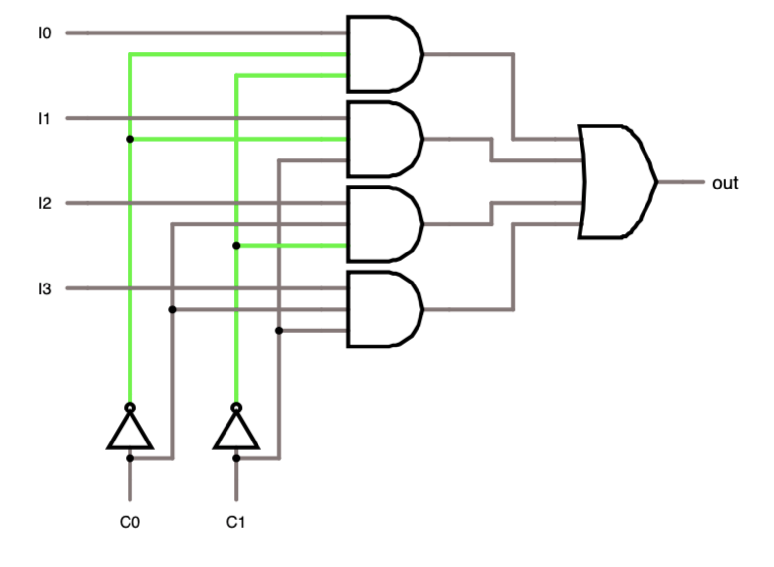
The multiplexer has 2 ^ n input lines, n control lines and one output line. In implementation, it is somewhat similar (Figure 1.5) to a decoder, if the decoder inputs are represented as control lines, each AND gate is supplemented with an additional input signal and the output values of all AND are combined by one OR. The essence of his work is to output a signal from only one of the possible input lines. A multiplexer is used for different purposes, for example, it can be useful for converting parallel code to serial. Suppose we have a parallel (this means that the lines operate simultaneously) a bus with several lines along which bits are transmitted in parallel; in order to read the word we need (usually the word width corresponds to the register bit capacity in the processor) we connect bus lines to the multiplexer inputs and sequentially switch on one input, say from top to bottom, thus the exact sequence of bits will go to the output.
The demultiplexer is a reverse multiplexer, it has one input line, n control lines and 2 ^ n output lines. The logic of his work is exactly the same as in the multiplexer, only one input signal goes to one of the output. Can be used to convert serial code into parallel.
Figure 1.5. Multiplexer
This type of circuit performs arithmetic operations on input signals. The main circuits are: logic functions, adder, shift scheme, ALU (ALU, Arithmetic Logic Unit).
Half-adder and full adder
The half-adder consists of two input and two output lines, the half-adder is a simple circuit (Fig. 1.6) of two gates: AND and EXCLUSIVE OR. By itself, a half-adder can add only one-bit values, but then why do we need a full adder? Basically, we want to add values with a higher bit depth, but we cannot satisfy this desire with only one half adder. When we add two one-bit values, we can overflow (Table 1.3. Last line of truth in the hyphen column). This is when the result of the operation does not fit in the same width as the input elements (in this case, 1). When two units are added, they get a deuce that cannot be stored in one bit, therefore it is necessary to transfer it in order to use it for further calculations, but since the half-adder does not provide for the use of two values and transfer at the same time, adding values with a bit more than one will not work . For example, suppose we add two 3-digit numbers, 5 (101 in binary) and 7 (111 in binary), the addition of two numbers begins with the lower digits, 1 and 1 are sent to the inputs of the half-adder, the output of the sum is 0 and the transfer output 1, this is where the problem arises, the following values, which should go to the half-adder, are 0 and 1, respectively, but what to do with the transfer, because there is no free entrance for it, but it cannot be discarded, therefore the half -matters cannot be directly used for additions.
The full adder has (fig. 1.7) three input lines and two output lines. Input transfer, as well as output, is used to enable combining adders into one with greater bit depth. The adder consists of two half adders, in order to build an adder of greater capacity, it is only necessary to combine adders through input and output carries.
Figure 1.6. Schema semi-adder.
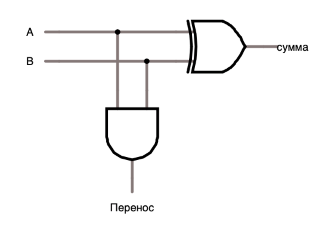
Table 1.3. The truth table is a half adder.
Figure 1.7. Scheme full adder.
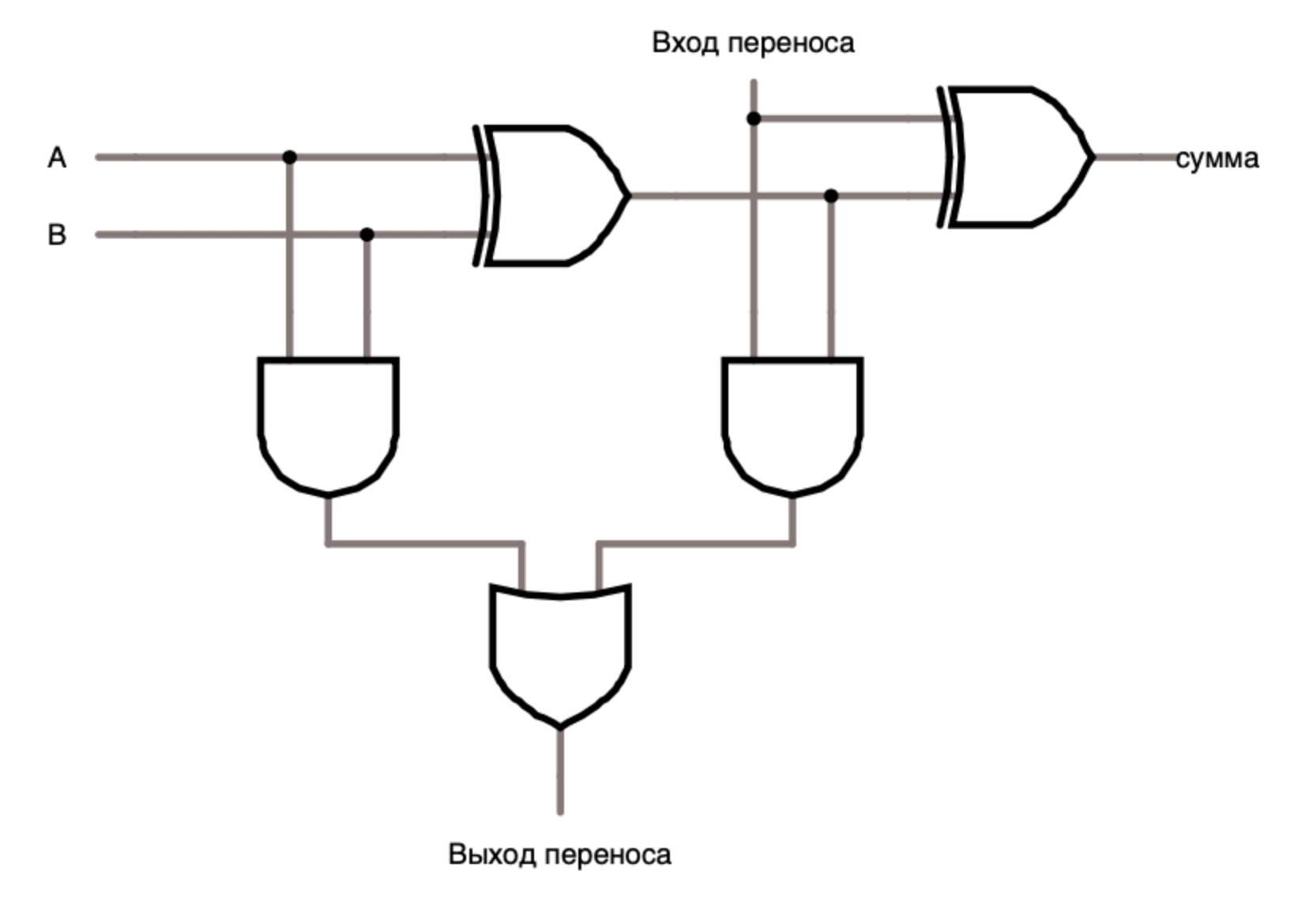
Table 1.4. Truth table of the full adder.
Shear pattern
The shift is necessary in order, for example, to perform multiplication (shift to the left) and division (shift to the right), but only with numbers that are powers of two (1, 2, 4, 8, etc.). The shift scheme (Fig. 1.8) should perform an offset one position to the left or right, depending on the direction bit. The direction bit (C), depending on its value, turns on certain Gates I. If it is 0 (left shift), the signal that goes directly (that is, does not pass through HE) will turn off the valve that is higher in the pair of two gates And one extreme valve And the bottom. The signal that passes through the NOT will turn on the lower valve in a pair of two AND valves and one extreme valve And from above. This means that the input values of In will only come out of the gates And the output signals, which are directed to the lower side; the high bit (I3) will be lost, since the lowest gate And will not pass the input signal further. A similar situation occurs when the direction bit is 1 (right shift), only the other AND gates will now be turned on and the signal will already be sent in the opposite direction (in this implementation), and therefore the right shift will occur.
Figure 1.8. Shear pattern
Arithmetic Logical Device
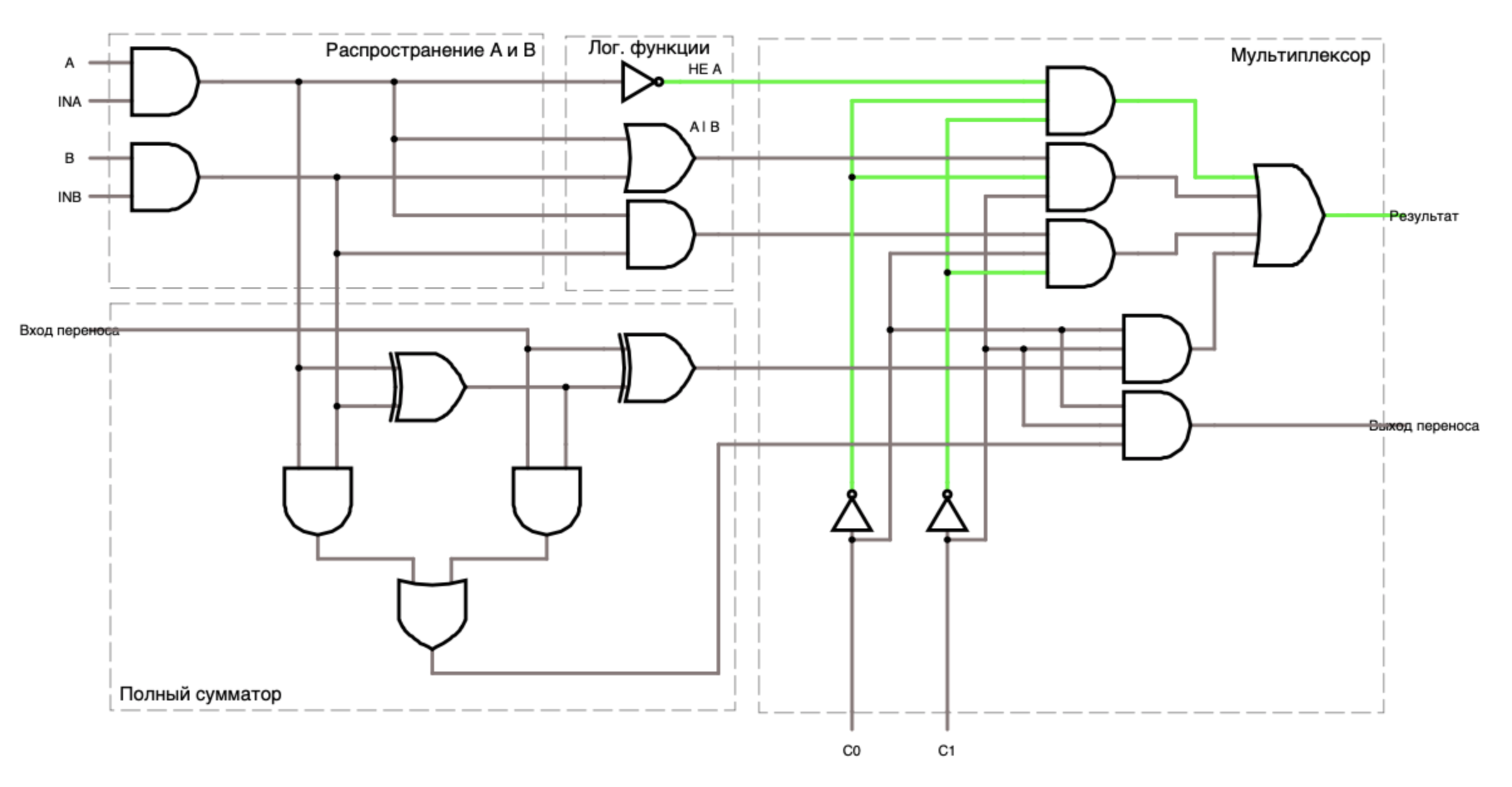
The ALU is a scheme (Fig. 1.9), which contains a multitude of arithmetic schemes, it is designed to store in one place all the operations necessary for any purpose. The implementation of the ALU is divided into several parts (in this implementation): the distribution of input operands, logic functions, an adder and a multiplexer. As we remember, the decoder should perform “switching on” operations, but here I decided to make a multiplexer, which supplies a value to the “Result” output, of only one of the four operations; two lower gates And in it they share the same combination in which the multiplexer works, this is necessary because the Transfer Output and Summa are part of the same operation, that is, both of these inputs should work only when summation is selected. Our ALU is designed to work with single-bit values, but it can be almost easily changed to a higher bit depth. Input lines INA and INB are designed to enable / disable A and B, respectively.
Figure 1.9. ALU scheme.
Also known as a microcircuit, these are the same circuits shown above, only they are placed in the case, which determines where the outputs for the signals should be located. This type of circuitry arose from the fact that it was not very advisable to sell individual circuits and gates: at least because there is no standard that says how, where, and in what quantity the input and output signals should be located.
There are a bunch of different types of enclosures, but we will look at the most famous ones:
Figure 2.0a, b, c. Types of buildings.


The memory output values depend not only on the input, that is, it is able to remember. Conceptually, all memory circuits are similar (Fig. 2.1), memory can “memorize” due to the fact that it is “closed”, that is, the upper gate depends on the output value of the bottom one, and the bottom one depends on the output value of the top one.
Figure 2.1. SR latch.

Before using the latch, it must be initialized. Initializing means translating it into a state where Q! =! Q is necessary for the latch to work correctly, that is, to correctly change its state (Q) between 0 and 1. To initialize, we need to apply S and R values at which the latch will go into a consistent state (Q! =! Q); when the latch is just starting to work, then there are any unknown values in Q and! Q, so the values of S and R should not depend on the values in Q and! Q. In other words, we need such values of S and R for which we obtain opposite values in Q and! Q.
We can consider the sequence of actions in different ways: we can assume that the signal arrives at S faster than R and then the upper gate will affect the result of the lower one; or vice versa, the signal reaches R faster, but this is not important, the results will be the same. In our example, I will assume that the signal S comes faster, and what next? What is the second value of the top valve? As mentioned above, we should not make assumptions about the value of Q (or! Q), so we should consider both situations: Q = 0 and Q = 1. Now all we have to do is check everything (Table 1.6) of the combination of S, R and Q.
Table 1.6. Table SR truth latch.
For SR latches built on the basis of OR-NOT (Fig. 2.1), the values for S and R will be 0 and 0, respectively, because the values in the columns “new Q! =! Q” and “Q == new Q” should be true immediately for Q = 0 and Q = 1. For example, when S = 0, R = 1, in the case of Q = 0, everything is in order, but when Q = 1, we change the state of Q from 1 to 0, and this should not be so, then without our knowledge the latch will change state. Similarly, it is possible to build an SR latch (and others) based on NAND, only initializing the values of S and R will have 1 and 1, respectively. Let's look at how initialization happens with values at Q = 0 and Q = 1.
When we send the signals 0 to the inputs S, R, and the value 0 is stored in Q, then two zeros 0 are not sent to the upper gate OR, it will have 1 output (Table 1.0). Further, the 0 and 1 do not arrive at the bottom valve OR, the output will be 0; that is, we have a non-conflicting latch state (Fig. 2.2a). In this case, the output value of the latch is 0 (Q), that is, it stores the value 0.
Alternatively, we can send signals 0 to the inputs S, R, and the value 1 is stored in Q. 0 and 1 arrive at the upper OR gate, which gives 0 at the output. 0 and 0 go to the lower OR gate, output will be 1; Again, we are in a non-controversial state of the latch (Fig. 2.2b). The output value of the latch is 1.
Figure 2.2. Two possible correct SR states of the latch.

The organization of the architecture of machines is represented as a series of levels, each of which is built on above the underlying level. This is done for a reason, with the help of a multi-tier architecture, we can abstract from the implementation and complexity of the lower level, thereby facilitating the design process and reducing the likelihood of errors. Abstraction is a key point in the entire computer architecture.
Computer organization consists of 6 levels: digital logic, microarchitecture, instruction set architecture (ISA), operating system, assembly language, applied, of course, except for the physical layer, which is below the digital logic level. I do not yet have plans to tell everything that happens above the level of ISA. There are two reasons for this: firstly, the purpose of these articles is not to consider all levels, but to show what levels 0-2 are, and, secondly, there is on habr'e Many articles on the levels above ISA and without me. This article will show the digital logic level, and in the next two microarchitecture and instruction set architecture, respectively.
Digital logic level
Digital logic level is essentially a set of logical functions that interact with each other to perform a larger task. All work at this level consists of two basic concepts: gates and Boolean algebra . First, I will talk about them, and then about the logic circuits and how they are used in the development, and finally, what the memory is and how it is implemented.
')
Valve
The gate (Fig. 1.0) is a device that receives input signals and provides output, it is implemented on transistors (I will not talk about their work). Gates are used at this level as a “building” material to represent basic logical operations, and then they are combined to implement certain schemes, that is, the meaning of this level is to build reusable circuits, and not about the operation of gates (and transistors) ; Further, on the basis of these schemes, more complex and highly specialized schemes can be built, for example, whole memory modules, different logic, for example, in order for CPU components to interact at the microarchitecture level, etc.
Figure 1.0. The image of the valves.
Table 1.0. Truth table for basic operations.
| A | B | AND | And NOT | OR | OR NO | ISK-OR |
|---|---|---|---|---|---|---|
| 0 | 0 | 0 | one | 0 | one | 0 |
| 0 | one | 0 | one | one | 0 | one |
| one | 0 | 0 | one | one | 0 | one |
| one | one | one | 0 | one | 0 | 0 |
Boolean algebra
This type of algebra works with 0 and 1, there are such operations (Table 1.0) as: AND (conjunction), OR (disjunction), NOT (denial), EXCLUSIVE OR, and their combinations, etc. You can use different methods to describe logical functions, but we will concentrate on only two: the truth table and the disjunctively normal form.
To build a truth table, we simply iterate over all combinations of the values of all variables. The table allows us to see all possible combinations in which the function takes the values of truth or false, it is suitable when we need such a property, for example, a decoder. The disjunctively normal form allows us to reduce its table size; for this, we use only those combinations of variable values for which the function takes only true values. To create a scheme that will take the true value only with the necessary combinations, we need to present these lines as minters .
Minterma is a logical function that takes a true value only with one set of values of variables included in it, it is realized by taking AND from all variables (with or without NOT). For example! A & B & C (! - NOT, & - AND) takes the true value only when A = 0, B = C = 1. When we present all true strings in the form of minters, we need to take from all the minters OR (disjunction). So now, combining all the above, we can implement the function in the form of a diagram.
For example, let's take the EXCLUSIVE OR function (Table 1.0). We see that it has two true lines: with A = 0, B = 1 and A = 1, B = 0. We take and present them as two mintherms,! A & B and A &! B. Indeed, the first minterma is equal to 1 only in the case when A = 0, B = 1; Another only in the case when A = 1, B = 0; Just the same with us, only such rows in the truth table take true values. Now that we have all the necessary mintermas, we take the OR operation from all the minters, that is, (A &! B) | (! A & B). We took and presented the function EXCLUSIVE OR in the form of a formula, which we can easily represent in the form of a logical scheme (Figure 1.1a), because it consists of simple functions: two AND and one OR. It would be more efficient if we reduced the number of inputs (Fig. 1.1b), for this you can combine A with! A into one input A, you only need to add another gate between the new input A and the old input! A NOT to allow the input signal for A was the opposite for old A and! A; We can do the same with B and! B.
Figure 1.1. An EXCLUSIVE OR Schema (the bar above the variable denotes NOT).
Logic
A logic circuit is a set of integrated valves with input and output signals. Figure 1.1 also shows a circuit in which the input signals are A and B, the output signal comes from the OR operation; it also has three valves: two AND, one OR. Now let's look at some types of schemes with which we need to meet in the future, these include: combinational, arithmetic, integrated circuits.
Combination schemes
A combination circuit is a circuit with one additional property: the values of the output signals depend only on the input, or in other words, there are no storage devices in it. Reusable components are created from this kind of circuits, which are used to implement most other circuits. We will consider several, namely: comparator, decoder, multiplexer / demultiplexer.
Comparator
A comparator has n input paired lines (i.e., 2n inputs) and one output line. The logic of his work is to compare each pair of bits (bits of the word A are compared with the corresponding bits of the word B) and, if one of them is unequal, return 0 (if 0 is false), otherwise 1. Let's build a truth table (Table. 1.1) for one-bit comparator; you can see that it is equal to the truth table EXCLUSIVE OR NOT (when NOT is added to the operation, then all output values in the table become opposite). Now let's expand it to a two-bit comparator, construct a truth table (Table 1.2) for it from two variable values of which depend on two single-bit comparators, that is, on two EXCLUSIVE OR NONE; in it, the value 1 in CMP0 (and CMP1) means that two inputs of a comparator are equal, 0 is vice versa, that is, 1 in the R column should be only when the values are equal in two comparators. This truth table coincides with the AND table, that is, we combine all the EXCLUSIVE OR NOT operation AND and we get a two-bit comparator (Fig. 1.3a). For further expansion of the comparator, it is only necessary to add EXCLUSIVE OR-NOT and connect it to I. The disadvantage of such an implementation is its redundancy, we need to add valves NOT for each EXCLUSIVE OR; we can get rid of this (Fig. 1.3b) if we replace the AND gate with NOT the inputs to OR-NOT, since their truth tables are the same.
Table. 1.1. Truth table for one-bit comparator.
| A | B | CMP |
|---|---|---|
| 0 | 0 | one |
| 0 | one | 0 |
| one | 0 | 0 |
| one | one | one |
Table. 1.2. Truth table for two-bit comparator.
| CMP0 | CMP1 | R |
|---|---|---|
| 0 | 0 | 0 |
| 0 | one | 0 |
| one | 0 | 0 |
| one | one | one |
Figure 1.3. Two schemes of two-bit comparators.
Decoder
The decoder has n input lines, 2 ^ n output, it is implemented so that the signal (true, 1) passes only to one output line. Each output gate AND receives its own combination of variable values that (values) are in some row of the truth table, and as we already know, the row of the truth table can be implemented as a minter, that is, we represent each row as the AND gate (Fig. 1.4 ) from several variables. The main use of a decoder is to selectively include different parts of a circuit (or circuits), for example, the ALU (about it later) has several operations that it can perform on input values to select one of them using a decoder.
Figure 1.4 Decoder.
Multiplexer / Demultiplexer
The multiplexer has 2 ^ n input lines, n control lines and one output line. In implementation, it is somewhat similar (Figure 1.5) to a decoder, if the decoder inputs are represented as control lines, each AND gate is supplemented with an additional input signal and the output values of all AND are combined by one OR. The essence of his work is to output a signal from only one of the possible input lines. A multiplexer is used for different purposes, for example, it can be useful for converting parallel code to serial. Suppose we have a parallel (this means that the lines operate simultaneously) a bus with several lines along which bits are transmitted in parallel; in order to read the word we need (usually the word width corresponds to the register bit capacity in the processor) we connect bus lines to the multiplexer inputs and sequentially switch on one input, say from top to bottom, thus the exact sequence of bits will go to the output.
The demultiplexer is a reverse multiplexer, it has one input line, n control lines and 2 ^ n output lines. The logic of his work is exactly the same as in the multiplexer, only one input signal goes to one of the output. Can be used to convert serial code into parallel.
Figure 1.5. Multiplexer
Arithmetic circuit
This type of circuit performs arithmetic operations on input signals. The main circuits are: logic functions, adder, shift scheme, ALU (ALU, Arithmetic Logic Unit).
Half-adder and full adder
The half-adder consists of two input and two output lines, the half-adder is a simple circuit (Fig. 1.6) of two gates: AND and EXCLUSIVE OR. By itself, a half-adder can add only one-bit values, but then why do we need a full adder? Basically, we want to add values with a higher bit depth, but we cannot satisfy this desire with only one half adder. When we add two one-bit values, we can overflow (Table 1.3. Last line of truth in the hyphen column). This is when the result of the operation does not fit in the same width as the input elements (in this case, 1). When two units are added, they get a deuce that cannot be stored in one bit, therefore it is necessary to transfer it in order to use it for further calculations, but since the half-adder does not provide for the use of two values and transfer at the same time, adding values with a bit more than one will not work . For example, suppose we add two 3-digit numbers, 5 (101 in binary) and 7 (111 in binary), the addition of two numbers begins with the lower digits, 1 and 1 are sent to the inputs of the half-adder, the output of the sum is 0 and the transfer output 1, this is where the problem arises, the following values, which should go to the half-adder, are 0 and 1, respectively, but what to do with the transfer, because there is no free entrance for it, but it cannot be discarded, therefore the half -matters cannot be directly used for additions.
The full adder has (fig. 1.7) three input lines and two output lines. Input transfer, as well as output, is used to enable combining adders into one with greater bit depth. The adder consists of two half adders, in order to build an adder of greater capacity, it is only necessary to combine adders through input and output carries.
Figure 1.6. Schema semi-adder.
Table 1.3. The truth table is a half adder.
| A | B | Amount | Transfer |
|---|---|---|---|
| 0 | 0 | 0 | 0 |
| 0 | one | one | 0 |
| one | 0 | one | 0 |
| one | one | 0 | one |
Figure 1.7. Scheme full adder.
Table 1.4. Truth table of the full adder.
| A | B | Login transfer | Amount | Output transfer |
|---|---|---|---|---|
| 0 | 0 | 0 | 0 | 0 |
| 0 | 0 | one | one | 0 |
| 0 | one | 0 | one | 0 |
| 0 | one | one | 0 | one |
| one | 0 | 0 | one | 0 |
| one | 0 | one | 0 | one |
| one | one | 0 | 0 | one |
| one | one | one | one | one |
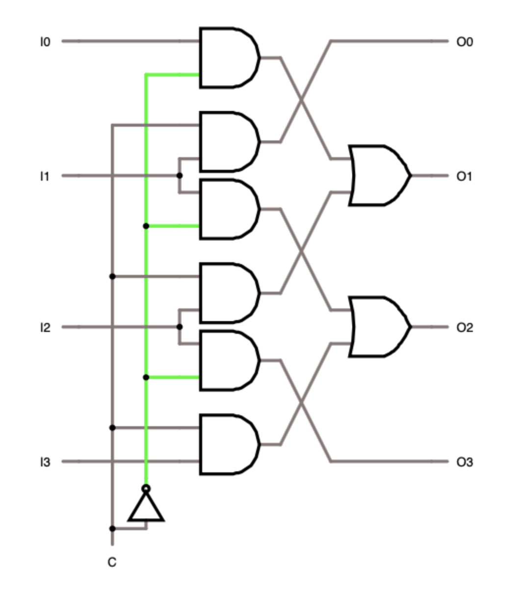
Shear pattern
The shift is necessary in order, for example, to perform multiplication (shift to the left) and division (shift to the right), but only with numbers that are powers of two (1, 2, 4, 8, etc.). The shift scheme (Fig. 1.8) should perform an offset one position to the left or right, depending on the direction bit. The direction bit (C), depending on its value, turns on certain Gates I. If it is 0 (left shift), the signal that goes directly (that is, does not pass through HE) will turn off the valve that is higher in the pair of two gates And one extreme valve And the bottom. The signal that passes through the NOT will turn on the lower valve in a pair of two AND valves and one extreme valve And from above. This means that the input values of In will only come out of the gates And the output signals, which are directed to the lower side; the high bit (I3) will be lost, since the lowest gate And will not pass the input signal further. A similar situation occurs when the direction bit is 1 (right shift), only the other AND gates will now be turned on and the signal will already be sent in the opposite direction (in this implementation), and therefore the right shift will occur.
Figure 1.8. Shear pattern
Arithmetic Logical Device
The ALU is a scheme (Fig. 1.9), which contains a multitude of arithmetic schemes, it is designed to store in one place all the operations necessary for any purpose. The implementation of the ALU is divided into several parts (in this implementation): the distribution of input operands, logic functions, an adder and a multiplexer. As we remember, the decoder should perform “switching on” operations, but here I decided to make a multiplexer, which supplies a value to the “Result” output, of only one of the four operations; two lower gates And in it they share the same combination in which the multiplexer works, this is necessary because the Transfer Output and Summa are part of the same operation, that is, both of these inputs should work only when summation is selected. Our ALU is designed to work with single-bit values, but it can be almost easily changed to a higher bit depth. Input lines INA and INB are designed to enable / disable A and B, respectively.
Figure 1.9. ALU scheme.
Integrated circuits
Also known as a microcircuit, these are the same circuits shown above, only they are placed in the case, which determines where the outputs for the signals should be located. This type of circuitry arose from the fact that it was not very advisable to sell individual circuits and gates: at least because there is no standard that says how, where, and in what quantity the input and output signals should be located.
There are a bunch of different types of enclosures, but we will look at the most famous ones:
- Dual Inline Package (DIP) is a case (Fig. 2.0a) in which the pins (input and output signals) are located on both sides parallel to each other, the number of pins in this case varies from 14 to 68 (only -in). This package is used for small and / or cheap circuits.
- Pin Grid Array (PGA) has the findings from all four sides (Fig. 2.0b).
- Land Grid Array (LGA) has a pin in the form of contacts across the entire (depending on the standard) area (lower part) of the case. LGA (Fig. 2.0c) has one important advantage over other cases: a large number of conclusions, which is especially important for such chips as processors. I note that the processor is not the same as the CPU, the processors are any microcircuit that makes the calculations, the CPU consists of the micro-architecture, in particular, the ALU and the control block.
Figure 2.0a, b, c. Types of buildings.
Memory
The memory output values depend not only on the input, that is, it is able to remember. Conceptually, all memory circuits are similar (Fig. 2.1), memory can “memorize” due to the fact that it is “closed”, that is, the upper gate depends on the output value of the bottom one, and the bottom one depends on the output value of the top one.
Figure 2.1. SR latch.
Before using the latch, it must be initialized. Initializing means translating it into a state where Q! =! Q is necessary for the latch to work correctly, that is, to correctly change its state (Q) between 0 and 1. To initialize, we need to apply S and R values at which the latch will go into a consistent state (Q! =! Q); when the latch is just starting to work, then there are any unknown values in Q and! Q, so the values of S and R should not depend on the values in Q and! Q. In other words, we need such values of S and R for which we obtain opposite values in Q and! Q.
We can consider the sequence of actions in different ways: we can assume that the signal arrives at S faster than R and then the upper gate will affect the result of the lower one; or vice versa, the signal reaches R faster, but this is not important, the results will be the same. In our example, I will assume that the signal S comes faster, and what next? What is the second value of the top valve? As mentioned above, we should not make assumptions about the value of Q (or! Q), so we should consider both situations: Q = 0 and Q = 1. Now all we have to do is check everything (Table 1.6) of the combination of S, R and Q.
Table 1.6. Table SR truth latch.
| S | R | Q | ! Q | new Q | new Q! =! Q | Q == new Q |
|---|---|---|---|---|---|---|
| 0 | 0 | 0 | one | 0 | one | one |
| 0 | 0 | one | 0 | one | one | one |
| 0 | one | 0 | one | 0 | one | one |
| 0 | one | one | 0 | 0 | 0 | 0 |
| one | 0 | 0 | 0 | one | one | 0 |
| one | 0 | one | 0 | one | one | one |
| one | one | 0 | 0 | 0 | 0 | one |
| one | one | one | 0 | 0 | 0 | 0 |
For SR latches built on the basis of OR-NOT (Fig. 2.1), the values for S and R will be 0 and 0, respectively, because the values in the columns “new Q! =! Q” and “Q == new Q” should be true immediately for Q = 0 and Q = 1. For example, when S = 0, R = 1, in the case of Q = 0, everything is in order, but when Q = 1, we change the state of Q from 1 to 0, and this should not be so, then without our knowledge the latch will change state. Similarly, it is possible to build an SR latch (and others) based on NAND, only initializing the values of S and R will have 1 and 1, respectively. Let's look at how initialization happens with values at Q = 0 and Q = 1.
When we send the signals 0 to the inputs S, R, and the value 0 is stored in Q, then two zeros 0 are not sent to the upper gate OR, it will have 1 output (Table 1.0). Further, the 0 and 1 do not arrive at the bottom valve OR, the output will be 0; that is, we have a non-conflicting latch state (Fig. 2.2a). In this case, the output value of the latch is 0 (Q), that is, it stores the value 0.
Alternatively, we can send signals 0 to the inputs S, R, and the value 1 is stored in Q. 0 and 1 arrive at the upper OR gate, which gives 0 at the output. 0 and 0 go to the lower OR gate, output will be 1; Again, we are in a non-controversial state of the latch (Fig. 2.2b). The output value of the latch is 1.
Figure 2.2. Two possible correct SR states of the latch.
Source: https://habr.com/ru/post/449190/
All Articles