Why silicon and why CMOS?
The very first transistor was bipolar and germanium, but the vast majority of modern integrated circuits are made of silicon using CMOS technology (a complementary metal oxide semiconductor). How is it that silicon has become the main of many well-known semiconductors? Why exactly CMOS technology has become almost a monopoly? Were there processors on other technologies? What awaits us in the near future, because the physical limit of the miniaturization of MOS transistors is actually reached?
If you want to know the answers to all these questions - welcome under cat. At the request of readers of previous articles I warn you: there is a lot of text, for half an hour.
Outside the year 1947 and 1948, John Bardeen and Walter Brattein, led by William Shockley at The Bell Labs, investigate the field distribution in germanium diodes and accidentally detect the transistor effect. And although the potential utility of the discovery looked obvious (however, urban legends say that the discovery was declassified after military experts saw no practical use in it), the first transistor looked like this:

Figure 2. Replica of the first transistor
')
Not very similar to a device suitable for industrial production, right? It took two years to make a capricious bipolar transistor more convenient in the production of a bipolar transistor from pn-junctions, after which the days (well, not days, but years) of electron tubes in mass electronic equipment were considered.
Of the three discoverers of the transistor, however, Shockley continued to work on them, who had little to do with the original work (because he was a theorist and boss, not a researcher), but he assumed all his fame and so because of this he quarreled with Bardin and Brattein, that they never again dealt with microelectronics. Brattein took up electrochemistry, and Bardin - superconductivity, for which he received the second Nobel Prize, becoming the only person in history who has two awards in physics.
Shockley, having successfully destroyed his research team with his ambitions, left Bell Labs and created his own Shockley Semiconductor Laboratory. The working climate in it, however, also left much to be desired, which led to the emergence of the famous “Treacherous Eight”, who fled from Shockley and founded Fairchild Semiconductor, which, in turn, became the parent of what we now know as “Silicon Valley” - including companies like Intel, AMD and Intersil.

Figure 3. Fairchildren - Fairchild based companies
Shockley himself never recovered from the G8's betrayal and rolled down the sloping: he was fired from his own company, carried away by racism and eugenics, became an outcast in the scientific community and died, forgotten by everyone. Even his children learned about the death from the newspapers.
The history of the opening of the transistor is widely known and described in many places. Much less is known that the first patent application for the transistor was not filed at all in 1947, but more than twenty years earlier, in 1925, by an American of Austro-Hungarian origin, Julius Lilienfeld. At the same time, unlike the bipolar transistor of 1947, the devices described in the patents of Lilienfeld were field: in the patent obtained in 1930, MESFET with a metal gate, and in the patent of 1933 - MOSFET, almost the same as we know it now. Lilienfeld proposed to use aluminum for the gate and aluminum oxide as a gate dielectric.
Unfortunately, the then level of technology development did not allow Lilienfeld to implement their ideas in prototypes, but the experiments conducted in 1948 by the same Shockley (already alone) showed that the patents of Lilienfeld described fundamentally efficient devices. Actually, the whole work of Shockley's group on the properties of diodes, which led to the accidental invention of a bipolar transistor, was part of the research to create a field-effect transistor, much more similar in properties to vacuum tubes and therefore more understandable to physicists of those years. Nevertheless, despite the successful confirmation of the efficiency of Lilienfeld’s ideas, in 1948 there was still no technology for stable production of thin defect-free films of dielectrics, while the bipolar transistor turned out to be quite more technological and commercially promising. MOS transistors were shelved, and bipolar devices began a triumphal march across the planet.
Minute of terminology
Bipolar transistor or Bipolar Transistor is a transistor in which both types of charge carriers, electrons, and holes are needed for operation, and which is controlled by the base current (multiplying it by the gain of the transistor). Usually made using pn junctions or heterojunctions, although the very first transistor, although bipolar, was not a transistor at the junctions. The popular English-language acronym is BJT, a bipolar junction transistor.
For transistors at heterojunctions (transitions between different materials, for example, gallium arsenide and gallium aluminitride), the acronym HBT (Heterojunction Bipolar Transistor) is used.
A unipolar or field effect transistor, also known as a Field-Effect Transistor or FET, is a transistor whose effect is based on the field effect and requires only one type of charge carrier. The field-effect transistor has a channel controlled by a voltage applied to the gate. Field effect transistors are quite a few varieties.
The MOSFET or MOSPT, which we are used to, is a transistor with a gate insulated from the channel using a dielectric, usually an oxide, which is a Metal-Oxide-Semiconductor structure (Metal-Oxide-Semiconductor). If you use a non-oxide, they can be called MISFET (I - Insulator) or MDPT (D - Dielectric).
JFET (J - Junction) or a transistor with a control pn-junction. In such a transistor, the field blocking the channel is created by applying voltage to the control pn junction.
The Schottky field effect transistor (PTSH) or MESFET (ME - Metal) is a JFET type that uses not a pn junction as a control but a Schottky barrier (between semiconductor and metal), which has a lower voltage drop and a higher operating speed.
A HEMT (High Electron Mobility Transistor) or high electron mobility transistor is a JFET and MESFET analogue using a heterojunction. These transistors are the most popular in complex semiconductors.

Figure 4. BJT, MOSFET, JFET
The first transistor was germanium, but technologists from different companies quickly switched to silicon. This was due to the fact that pure germanium is actually quite poorly suited for electronic applications (although germanium transistors are still used in audio equipment, mowing under the old days). The advantages of germanium include the high electron mobility and, most importantly, holes, as well as the firing voltage of pn junctions in 0.3 V versus 0.7 V in silicon, although the latter can be leveled by using Schottky junctions (as was done in TTLSh logic) . But because of the smaller width of the forbidden zone (0.67 vs. 1.14 eV), germanium diodes have large reverse currents, which increase strongly with temperature, which limits the temperature range of applicability of germanium circuits, and the allowable powers (for small ones, the influence of reverse currents is too large; interfere with self-heating). On top of the temperature problems of germanium, its thermal conductivity is much lower than that of silicon, that is, it is more difficult to remove heat from powerful transistors.
Even in the early period of the history of semiconductor electronics, germanium devices had big problems with yield due to the difficulty of obtaining pure crystalline germanium without screw dislocations of the lattice and poor surface quality, unlike silicon, which is not protected from external influences by oxide. More precisely, germanium has an oxide, but its crystal lattice coincides with that of pure germanium much worse than that of silicon, which leads to the formation of an unacceptably large number of surface defects. These defects seriously reduce the mobility of charge carriers, negating the main advantage of germanium over silicon. And to top it off, germanium oxide reacts with water, both during chip production and operation. However, the rest of the semiconductors are even less fortunate, and they have no oxide at all.
Trying to solve the problem of poor germanium surface, which prevented the field-effect transistor from being made, Shockley thought up to remove the channel to the depth of the semiconductor. So a field-effect transistor with a pn-junction control, also known as JFET, appeared. These transistors quickly found their place in analog circuits - primarily due to the very small input current (compared to bipolar transistors) and good noise characteristics. This combination makes JFET an excellent choice for an input amplifier stage - as can be observed, for example, in this article by Ken Shirriff. Moreover, when integrated circuits were made instead of individual components, JFET turned out to be quite well compatible with bipolar technology (I even made JFET from a bipolar transistor in the figure above), and they became a common place in analog bipolar process technology. But all this was already on silicon, and germanium remained forgotten for many years, until it was time to strengthen the position of silicon instead of fighting with it. But more on that later.
And what about MOS transistors? It seemed to be forgotten for almost a decade due to the rapid progress of bipolar counterparts, they nevertheless developed. In all the same Bell Labs in 1959, Davon Kang and Martin Attala created the first working MOS transistor. He, on the one hand, almost directly realized the idea of Lilienfeld, and on the other, immediately turned out to be almost identical to many next generations of transistors using silicon oxide as a gate dielectric. Unfortunately, Bell Labs did not recognize the commercial potential of the invention at that time: the prototype was significantly slower than the bipolar transistors of that time. But the potential of the novelty was recognized in Radio Corporation of America (RCA) and Fairchild, and already in 1964, MOS transistors hit the market. They were slower than the bipolar counterparts, worse amplified, noisy and very suffering from electrostatic discharge, but they had zero input current, low output resistance and excellent switching capabilities. It is not so much, but it was only the beginning of a very long journey.
In the early stages of the development of semiconductor electronics, analog and radio frequency applications dominated: the word "transistor" for a long time meant not only the actual transistor, but also a radio receiver based on it. Digital computers based on one or two gates of microcircuits were huge (although they could not be compared with tube lamps), so there were even attempts to make calculations in an analog way - it’s good enough to implement integration or differentiation with just one operational amplifier instead of a whole placer of digital chips . But digital computing turned out to be more convenient and practical, as a result of which the era of digital electronic computers began, which continues today (although quantum computing and neural networks have already achieved significant success).
The main advantage of the MOS technology of that time was simplicity (let me remind you that until the eighties each microelectronic company had to organize its own production): to implement the simplest working n-MOS or p-MOS scheme, only four photolithographs are needed, for CMOS - six, and for a bipolar lithography scheme, seven are needed for one type of transistor, and more accurate control of diffusion and, ideally, epitaxy is still needed. Fat minus was the speed: MOSFETs lost in comparison with bipolar and JFET more than an order of magnitude. At the moment when CMOS allowed to reach the frequency of 5 MHz, it was possible to make 100-200 on ECL. There is no need to talk about analog applications - MOSFETs are very poorly suited for them because of low speeds and low gain, while a bipolar circuit with JFET at the inputs is capable of providing almost all designer requests.
While the degree of integration of microcircuits was small, and the power consumption was not considered by anyone especially, the advantage of emitter-coupled logic (ECL) for high-performance applications was obvious, but the MOS-technology had some trump cards up its sleeve that played a little later. In the sixties, seventies and eighties, MOS and bipolar processes developed in parallel, with MOS used exclusively for digital circuits, and bipolar technology for both analog circuits and logic based on the TTL (transistor-transistor logic), and ECL families.

Figure 5. Cray-1, the first supercomputer of Seymour Kray, presented to the public in 1975, weighed 5.5 tons, consumed 115 kW of energy and had a performance of 160 MFLOPS at 80 MHz. It was built on four types of discrete ECL chips, and contained about 200 thousand gates. The chip on which the logic was built is the Fairchild 11C01, a dual valve that contains the elements 4ILINE and 5ILINE, and consumes 25-30 mA of current at a power of -5.2 V.
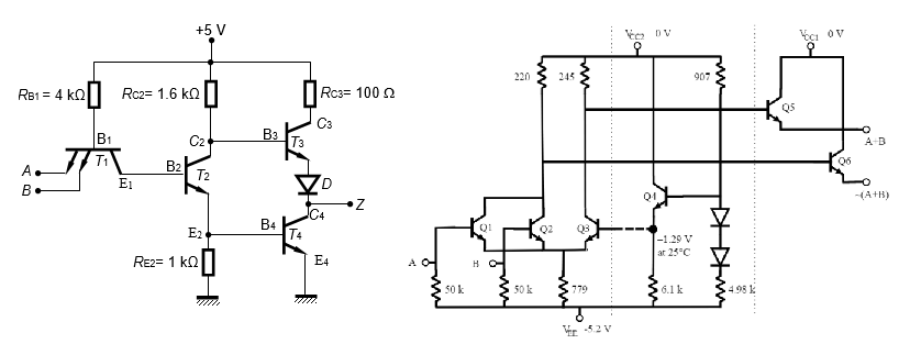
Figure 6. Logic element 2INE on TTL and 2IL / ILINE on ECL
Note that the ECL logic element is simply an amplifier with no feedback, built in such a way that the switching transistors are always in the “fast” linear mode and never fall into the “slow” saturation mode. The charge for speed is the current that constantly flows through the circuit, regardless of the operating frequency and the state of the inputs and outputs. It's funny, but some time ago they began to try to use this disadvantage as an advantage: due to the constant current consumption, ECL cryptographic schemes are much more resistant to hacking through “listening” to the current consumption than CMOS, where the current consumption is proportional to the number of valves switching at a given time . If you replace the bipolar transistors with field (JFET or MESFET), you get ISL - source-related logic, which also found its use in complex semiconductors.
Obvious plus nMOP or pMOP logic is simplicity of manufacture and a small number of transistors, which means a small area and the ability to place more elements on the chip. For comparison: the element 2INE or 2ILINE on nMOP / pMOP consists of three elements, on CMOS - of four. On TTL, these elements contain 4-6 transistors, 1-3 diodes and 4-5 resistors. On ECL - 4 transistors and 4 resistors (in this case, it is convenient to make OR and NOR, and inconveniently AND and NAND). Pay attention, by the way, that all transistors on the circuit of TTL and ECL elements are npn. This is because making a pnp transistor in a p-substrate is more complicated than npn, and their structure is different - unlike CMOS technology, where the transistors of both types are almost the same. Moreover, both pMOS and bipolar pnp, working at the expense of holes, were slower than their “electronic” counterparts, and therefore in bipolar logic, whose main goal was speed, they were not in the yard.
The second important advantage of the MOS-technology, which manifested itself in full during the transition to CMOS and which largely determined the dominance of this technology, is low power consumption. The CMOS valve consumes energy only in the process of switching, and it does not have static power consumption (for modern technologies this is not so, but we omit particular ones). Typical operating current of the ECL valve is from 100 μA to 1 mA (0.5-5 mW at a power supply of 5.2 V). Multiplying this number by, say, a billion gates that make up modern Intel processors, we get MegaWatts ... Actually, you saw the Cray-1 consumption higher. However, in the eighties, it was usually about thousands or tens of thousands of gates, which, in theory, made it possible to keep within a reasonable power budget, even with bipolar logic. In practice, however, the same area of the crystal was placed several times larger than CMOS valves, which consumed less power, and became much faster with a decrease in design norms (Moore's law worked with might and main).
Intel 8008 (1972) on a ten-micron PMOS technology operated at a frequency of 500 kHz (versus 80 MHz for a much more complex Cray-1 system), Intel 8086 (1979) on a three-micron NMOS and later CMOS accelerated to 10 MHz, and the original 80486 ( 1989) - right up to 50 MHz.
What made designers continue to try bipolar designs, despite the rapid reduction in the difference between them and CMOS, and despite the power consumption? The answer is simple - speed. At the dawn of time, the additional great advantage of ECL was the minimal loss of speed when working on large capacitive loads or long lines — that is, an assembly from many cases with ECL logic was much faster than an assembly on CMOS or TTL. Increasing the degree of integration allowed CMOS to partially overcome this drawback, computing systems were still multi-chip, and each output of the signal outside the crystal (for example, to the external cache) slowed down everything. Even in the late eighties, bipolar valves were still significantly faster, for example, due to several times less voltage difference between logical zero and logical unit - 600-800 mV for ECL versus 5 V for CMOS, and this is when the size of transistors is bipolar technologies have already begun to lag behind CMOS. But if CMOS scaling went in such a way that the specific power per unit area of the chip remained constant (this phenomenon is a “consequence” of Moore's law and is called “Dennard scaling”), then the power of ECL almost did not fall, because for fast work static operating currents are needed. As a result, developers of digital circuits began to prefer CMOS for the implementation of increasingly complex computer architectures, even where great performance was needed.
Assistance to digital bipolar technology has come from no waiting. In the early eighties, a RISC concept was invented, implying a significant simplification of the microprocessor and a reduction in the number of elements in it. Bipolar technologies somewhat lagged behind CMOS in the degree of integration, because bipolar LSIs were mostly analog, and there was no big reason for rushing for Moore's law. Nevertheless, the beginning of the development of RISC coincided with the moment when it became realistic to pack an entire processor on a single chip or at least two or three (the cache was usually external). In 1989, Intel 80486 came out, in which the FPU was made on the same chip as the main processor - it was the first chip that used more than a million transistors.
By the time in question, many chip manufacturers began to switch to the Fabless model, providing the organization of production to other companies. The development of integrated microprocessors on ECL resulted in the activities of one of these companies. The company was called Bipolar Integrated Technology and was never particularly successful, from its founding in 1983 to selling to PMC-Sierra in 1996. There is a suspicion that the bet on failure was precisely the rate for bipolar digital products, but in the late eighties it was not so obvious , and the company had bipolar processes that were advanced in size and degree of integration. Their first proprietary product was the FPU coprocessor chip, and BIT actively collaborated with two RISC pioneers, MIPS Computer Systems and Sun Microsystems, in order to create chips based on RISC architectures for which this coprocessor would be useful. The first implementation of the MIPS II architecture - a set of R6000, R6010 and R6020 chips - was implemented on ECL and produced at BIT facilities. They also produced a SPARC B5000 processor.
Somewhat later, DEC implemented MIPS II on a single chip on Motorola bipolar technology. So, imagine: in the yard in 1993, the leading Intel product is that Pentium (800 nm CMOS technical process, 66 MHz clock speed, 15 W TPD, three million transistors per chip). The IEEE Journal of Solid-State Circuits has an article entitled “ A 300-MHz 115-W 32-b Bipolar ECL Microprocessor ”. Three hundred (!) Megahertz and one hundred and fifteen (!!!!) Watt. A separate article, of course, was devoted to the body and heat sink of this monster. I highly recommend reading both articles if you have access to the IEEE library - this is an excellent document of the era, which contains phrases of the scale of the design team and circuit performance has been increased. "byte-loop circuits and wired-OR circuits)". Okay, CAD, only lazy did not write it yourself in 1993 (ask YuriPanchul , he will confirm), but wired OR!

Figure 7. Photograph of a DEC processor chip and its case with a heat sink
Gallium arsenide is one of the first complex semiconductors to attract the attention of the microelectronic industry. The main advantage of gallium arsenide both over germanium and silicon is the enormous mobility of electrons. At the same time, it also has a fairly wide forbidden zone, which allows it to operate at high temperatures. The ability to operate at frequencies of hundreds of MHz or even several GHz, while tens of MHz are being squeezed out of silicon - is this not a dream? Gallium arsenide has long been considered the “material of the future,” which is about to replace silicon. The first MESFET was created on it in 1966, and the last active attempts to make an LSI on it were made already in the mid-nineties at the Cray Corporation (they buried it completely) and on the Micron (K6500 chip series).
An important problem that had to be solved was the absence of native oxide in gallium arsenide. But is it a problem? After all, if there is no oxide, then there are no problems with radiation resistance!It is for these reasons that programs for the development of arsenide gallium technology have been heavily funded by the military. The results on durability were really excellent, but with the actual technology came out a little more difficult. The need to use JFET means either the use of LIS - fast, but very much consuming, or JFET instead of MOSFET in imitation of nMOP-logic - simpler, but not so fast and still fairly consuming. Another nasty little thing - if you do nothing, then JFET on gallium arsenide is normally open, that is, their threshold voltage is below zero, which means more power consumption than it would be on a MOSFET. In order to make normally closed transistors, technologists need to try pretty hard. However, this problem was solved relatively quickly,and in GaAs logic, ED JFET technologies began to be actively applied with normally closed (E - enhancement) active transistors and normally open (D - depleted) in loads. Another disadvantage that was greatly underestimated initially was that gallium arsenide has a very high mobility of electrons, but not holes. You can do a lot of interesting things on nJFET (for example, high-frequency amplifiers), but with 1 mW per valve it is quite difficult to talk about VLSI, and if you make low-consuming complementary circuits, they will be even slower than silicon due to low mobility.You can do a lot of interesting things on nJFET (for example, high-frequency amplifiers), but with 1 mW per valve it is quite difficult to talk about VLSI, and if you make low-consuming complementary circuits, they will be even slower than silicon due to low mobility.You can do a lot of interesting things on nJFET (for example, high-frequency amplifiers), but with 1 mW per valve it is quite difficult to talk about VLSI, and if you make low-consuming complementary circuits, they will be even slower than silicon due to low mobility.
And again, as with the bipolar schemes, the concept of RISC in the person of the same MIPS architecture came to the aid of the military who wanted very much to obtain radiation resistance. In 1984, DARPA signed three contracts for the development of GaAs MIPS microprocessors - with RCA, McDonnell Douglas and the CDC-TI collaboration. One of the important requirements of the technical specification was the limitation of 30 thousand transistors, with the wording “so that the processors could be started to be mass-produced with an acceptable yield.” In addition, there were options for conversion to gallium arsenide of the Am2900 family from AMD, fast-resistant arsenide gallium versions of the legendary 1802 microcontrollers from the same RCA, basic matrix crystals for several thousand gates and static memory chips for several kilobits.
, 1990 , MIPS , SPARC — LEON MIPS. , LEON ARM, - . ARM- . , . , , Elsevier .
The most interesting decision in my opinion was a group from McDonnell Douglas. I traced through the publications in IEEE Transactions on Nuclear Science the history of their project (search by the name Zuleeg), from the first transistors in 1971 to my own complementary JFET technology and chips based on it in 1989. Why is it complementary? Because most of the microprocessor (both in terms of the transistor budget and power budget) is cache memory, and the delay of the memory cell itself is not always a factor limiting performance, but the gain in power consumption when using a complementary cell is obvious. By making complementary cache and nJFET logic, McDonnell Douglas obtained an excellent ratio of speed and consumption - and radiation resistance literally to surrender, without any additional effort.
And everything would be fine, but at the same time when the account of transistors in arsenide gallium microprocessors went to tens of thousands, relatively inexpensive silicon CMOS chips with millions of transistors were already available on the commercial market, and the lag continued to grow. Even the developers of the “material of the future” among numerous stories about achievements wrote in their articles the phrases “a yield percentage of 3% would be achieved, that is, one suitable chip from a plate with a diameter of 75 mm”, or “if we reduce the density of defects to such and such level, we will be able to increase the percentage of yield from 1% to 10%, ”and such figures appear in unrelated scientific groups from different countries. The capriciousness of gallium arsenide and the fragility of its crystal lattice,interfering with growing large-diameter crystals and limiting dopant levels is well known, and this, combined with the desire to minimize the number of transistors on a microprocessor chip, leads me to believe that such a low yield for gallium arsenide was indeed the norm, and not only in the laboratory, but also in mass production. Moreover, according to the already Soviet data, the final cost practically did not depend on the complexity of the technology, because the gallium arsenide plates themselves were more expensive than any processing. It is not surprising that no one but the military had such SBIS.and not only in the laboratory, but also in mass production. Moreover, according to the already Soviet data, the final cost practically did not depend on the complexity of the technology, because the gallium arsenide plates themselves were more expensive than any processing. It is not surprising that no one but the military had such SBIS.and not only in the laboratory, but also in mass production. Moreover, according to the already Soviet data, the final cost practically did not depend on the complexity of the technology, because the gallium arsenide plates themselves were more expensive than any processing. It is not surprising that no one but the military had such SBIS.
Until now, the article has been telling about the successes and failures of American companies, but microelectronics was not only in America, right? Unfortunately, there is little to tell about the difficult path of Soviet microelectronics in the choice of technologies. The first reason is that the history of American (and, for example, Japanese) developments is well documented by publications in IEEE specialized journals, whose archive is now digitized, and studying them is a real pleasure for connoisseurs. Soviet microelectronics was extremely closed throughout its history. There were few publications even in Russian, not to mention reporting our successes to the whole world (which was done, for example, in fundamental physics). And even the little that has been published is now very difficult to find and, of course, only in paper form, and not in electronic form. Therefore, by the way,it is now a pleasure to see Russian colleagues at international scientific conferences and industrial exhibitions, not only as guests, but also as speakers. The second reason is that most of the time, Soviet microelectronics, albeit only slightly, lagged behind the Americans and actively engaged in copying successful Western developments. Moreover, since the early eighties, when the world began all the most interesting, the Ministry of Electronic Industry of the USSR officially headed for the rejection of the original development and universal copying of American microchips - already serial, rather than experimental developments and methods. Perhaps, in the conditions of limited resources, this was the right decision, but its result was an increase in the backlog (and not a technological one, but an ideological one),which, after the collapse of the USSR, became virtually irreversible - until, as early as the twenty-first century, Russian microelectronics was “restarted” virtually from scratch.
As a result, although GaAs medium integration chips were used in the early nineties, both in Cray and EMU EC-4 supercomputers, in the USSR there were never RISC processors that played an important role in the final stages of the struggle between CMOS, ECL and gallium arsenide. From a technological point of view, at the same time that Americans were developing single-crystal microprocessors, the Zelenograd “Micron” put into mass production an arsenide-gallium K6500 chip series, which included memory up to 16 kbps, basic matrix crystals up to ten thousand gates and a microprocessor kit Of the five chips - that is, the same complex crystals as the American processors. But if McDonnell Douglas, using normally closed JFETs of both types of conductivity, simulated GaAs nMOP and CMOS circuits,aimed at minimizing energy consumption and preparing the ground for increasing the degree of integration, the K6500 was very fast (up to 1 GHz), but much more complex and capricious schemes on the LIS with normally open MESFET (which makes the results achieved by the degree of integration even more surprising).

Figure 8. Two variants of McDonnell Douglas technical processors inverters and K6500 series inverter chips
Gallium arsenide work continued on Micron from 1984 until at least 1996, but I couldn’t find any information about what happened after that. Now all the development of "Micron", including radiation-resistant and radiofrequency, are made on silicon.
Developers of silicon CMOS special-purpose microcircuits, meanwhile, were not standing still; By the early nineties, it became clear that to provide radiation resistance on slightly modified commercial silicon CMOS technology is not much more difficult than on expensive and capricious gallium arsenide, which deprived it of the last important advantage and limited it to very narrow and specific niches - mainly discrete microwave and power devices. . Moreover, even in these applications, not arsenide, but gallium nitride or a variety of heterostructures with better temperature characteristics, higher mobility, and a larger breakdown field, are now increasingly being used.

Figure 9. Comparison of the basic properties of silicon, gallium arsenide and gallium nitride for power and microwave applications
And what, you ask, can VLSI be made on gallium nitride? Unfortunately, gallium nitride also has a low hole mobility, and not only that. Radically larger than silicon, hole mobility is possessed only by indium antimonide, but it has such a narrow forbidden zone that devices based on it can work only at cryogenic temperatures.
Don't get me wrong, other semiconductors are also needed, and they have many useful uses. When in 2000 the Nobel Committee finally decided to give out an award for electronics, Jack Kilby received one half of the award for creating the first integrated circuit, and the second for Zhores Alferov and Herbert Kremer for “developing semiconductor heterostructures used in high-frequency circuits and optoelectronics”. Our life is hard to imagine without lasers on heterostructures, the markets for power devices on gallium nitride and silicon carbide are growing like yeast (and on electrification of transport), the rapid deployment of 5G networks operating at frequencies up to 39 GHz is impossible to imagine without semiconductors A3B5, but only Silicon CMOS technology turned out to have all the necessary properties to create computational VLSI,constituting the lion’s share of the microelectronics market and managing all the diversity mentioned above.
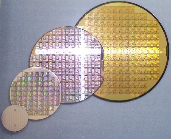
However, even silicon microelectronics is much wider than only high-performance microprocessors. Right now, TSMC simultaneously with the commissioning of the 5 nm process technology launches a new factory with design standards of 180 nm on 200 mm plates - because the demand for them is there and it is growing steadily. Yes, this market is much smaller than the market of chips for mobile phones, but the investments to enter are much more modest. The same can be said about the markets for silicon carbide and gallium nitride. And it is precisely complex semiconductors, microwave and power electronics, in my humble opinion, can become a real driver for the revival of Russian microelectronics and its entry into the world market. In these areas of competence and equipment of Russian companies are very strong and quite close to world leaders. Everything in the course about 180, 90 and 65 nm on the “Micron”,but few have heard of 200 nm on the “Source” or 150 nm on the “Mikran”. Few people have heard that the STM factory in Catania, from which the 180 nm process at Micron was copied, has now completely switched to the production of silicon carbide, whose market should reach three billion dollars in five years. STM recently bought a manufacturer of SiC substrates to own the entire production chain, and in principle do everything to become leaders in the growing market.to be in a growing market leader.to be in a growing market leader.
The articles of the late eighties and early nineties, devoted to promising technologies - ECL on silicon, complementary to JFET on GaAs, attempts to make germanium great again - almost invariably end with the words “we have demonstrated excellent perspectives of our idea, and literally a couple of years, when technology has developed a little more and allow more transistors on a chip / less consumption / higher yield percentage, that's when we conquer the world. ” Here are just the promised progress in the money DARPA never came. Why? Because the microcircuit production technology rises in price with each new reduction in size, and no research grants could kill the volume of investments by Intel, which worked on the huge consumer market and understood well that technological leadership is one of the keys to commercial leadership. That is why Intel raised the flag of Moore's law and appointed themselves responsible for its implementation, after which all other manufacturers were dragged into a crazy arms race that small companies and other technologies could not predictably afford. As a result, Intel has exactly one competitor in the niche of personal computers, and in general, only three companies in the world - TSMC, Intel and Samsung have technology below 14 nm. We can say that Intel was very lucky to start working with MOS transistors long ago, and not with ECL, but if they were not lucky, someone else would have been lucky, and the result would have remained about the same.
The fact that the advantage of CMOS on silicon is indisputable has become clear by the end of the nineties, and the disproportion of resources invested in it and everything else has become such that, instead of developing new technologies for specific needs, it has become more profitable and easier to attach the appropriate attachments to CMOS. BiCMOP technology with bipolar npn transistors appeared for designers of analog circuits, nonvolatile memory for embedded electronics, high voltage DMOS transistors for power applications, SOI substrates for high temperatures or high speeds, and integrated photodiodes for optoelectronics. The system-on-chip concept has become an important driver for the integration of additional options into CMOS technology. If earlier the system designer chose suitable chips based on how well they coped with the objective functions, not paying attention to the technology of their production (in the worst case, level translators were still needed, but this is not terrible), then with the increasing degree of integration place all components of the system on a single chip and thus kill many birds with one stone - increase the speed and reduce consumption due to the lack of need to pump capacitance tracks on the PCB, increase t chnost by better matching elements to increase reliability by reducing the number of soldering points. But for this, all parts of the system had to be CMOS compatible. The factories responded to this “whatever you like - just pay for additional masks and technology options” and started putting specialized technical processes into production one by one. Additional masks - expensive and difficult, and the chip should be cheap? And here the textbooks on analog design are already being rewritten from good and fast bipolar transistors to bad and slow field ones. Not enough speed for the microwave? Try gallium arsenide again? No, let's stretch the crystal lattice of silicon with germanium to locally increase the electron mobility. Sounds hard? But this is CMOS compatible! A cheap microcontroller with flash memory and an ADC on one chip sounds much nicer than the same on three chips, right? Digital data processing and control on the same chip as the analog part of the system became a key achievement that allowed microcontrollers to penetrate everywhere, from deep space to the electric kettle.

Figure 10. Schematic section of BCD technology
My favorite example of this kind is BCD technology. BCD is Bipolar (for analog part), CMOS (for digital), DMOS (high-voltage switches on the same chip as the control logic). Such technologies are able to work with voltages up to 200 volts (and sometimes more) and allow you to implement everything on a single chip for controlling electric motors or DC / DC conversion.

Figure 11. Section of SOI BCD with high-voltage LDMOS transistor in an insulated pocket
The BCD SOI technology complements all of the above with complete dielectric isolation of elements, improving thyristor resistance, noise isolation, increasing operating voltages, allowing you to place high-side keys on a chip without problems or, for example, work with negative voltages (needed for powerful GaN keys with a threshold below zero volt). On the same chip, manufacturers offer to place non-volatile memory, IGBT, Zener diodes ... the list is long, you can play bullshit-bingo at presentations) Pay attention to the depth of the silicon layer: unlike the "ordinary" SOI technologies, where it is tried to be minimized to get rid of from the bottom of the stock and source pn-junctions and increase the speed of work, the silicon layer in BCD is very deep, which helps to ensure acceptable resistance to electrostatic discharge and thermal characteristics. At the same time, transistors behave exactly like voluminous ones, only with full dielectric isolation. This, in addition to the target audience from manufacturers of car electronics, is also used to create its own non-high-voltage, but radio-resistant CMOS chips, for example, Milandr or Atmel, receiving the main advantage of SOI without its usual drawbacks.
Even when Moore's law began to break due to the fact that reducing the size of silicon transistors came to physical limits, it turned out that it was more profitable to continue to bring CMOS to mind than to look for something fundamentally new. Of course, they invested money in the research of alternatives and ways of escape, but the main efforts were thrown out to improve the silicon CMOS and ensure the continuity of developments. For the discovery of graphene, Novoselov and Heim were given the Nobel Prize almost ten years ago; and where is that graphene? That's right, in the same place where carbon nanotubes and all other materials of the future, and production on the 5 nm process has already begun on silicon, and everything goes to the fact that there will also be 3 or even 2 nm. Of course, this is not really real nanometers (which I already wrote about here on Habré), but the packing density continues to grow; albeit very slowly, but it is still silicon CMOS.

Figure 12. Gate All Around Samsung Transistors for 5nm technology and below. The next step is compared to FinFET and the answer to the question "why not pack transistors in several layers?" All the other methods have been exhausted, now it is the turn of several layers. Put seven of these transistors vertically, we get one nanometer instead of seven!
Even silicon oxide, for the sake of which everything was originally started, fell victim to progress in CMOS! He was replaced by complex multilayer structures based on hafnium oxide. Germanium was added to the channel to increase mobility (already tested in developments for BiCMOP microwave); they even go so far as to test (for the time being only test) in n-type “silicon” transistors from A3B5 materials (which have high electron mobility), and p-types from germanium (which has high hole density). About trivia such as changing the form of a channel from flat to volumetric (FinFET) and marketing tricks with design code numbers, writing is not enough.
What awaits us in the future? On the one hand, the progress of silicon technology with the introduction of EUV lithography and Gate All Around transistors has precisely exhausted itself; the gap from the plans of the ITRS of twenty years ago is about ten years, Intel has long since abandoned its famous “tick-toe”, Globalfoundries and completely refused to fall below 14 nm. The cost of a transistor on a chip has passed at least at the norms of 28 nm and since then began to grow. And most importantly, the target markets have changed. For many years, the driver for reducing project standards was the personal computer market, then the personal computers changed to mobile phones (around this time, TSMC and Samsung caught up with Intel). But now and in the market of mobile phones recession and stagnation. There was a short-term hope for mining chips, but it did not seem to come true.
New favorite chip manufacturers - the Internet of things. Indeed, the market is large, fast-growing and with good long-term prospects. And most importantly - for the Internet of things, performance and the number of elements on a chip are not critical competitive advantages, but low power consumption and low cost are. This means that the main reason for reducing design standards has disappeared, but there are reasons to optimize the technology for specific tasks. Sounds interesting isn't it? Something like ... a press release from Globalfoundries about stopping work at 7 nm and a concentration at 14/12 and 28/22 nm FDSOI. Moreover, the rise in price of new technologies in combination with tough price competition has led to the fact that microchip manufacturers are in no hurry to switch to new design standards simply because they can, and stay on the old ones for as long as it is reasonable to do, and also combine heterogeneous chips - but now not on the board, but in the inside of the case. "System on a chip" was replaced by a "system in the case" (I also wrote about this in more detail ). The appearance of systems in the case and the Internet of things, among other things, give a new chance to complex semiconductors, because placing an arsenide gallium chip in one case with silicon does not interfere anymore, and the need for a radio path in the system for the Internet of things is quite obvious. The same applies to a variety of optical devices, MEMS, sensors - and in general everything that exists in microelectronics in addition to CMOS on silicon
So my forecast for the further development of CMOS silicon technology and its substitutes will be that we will see a radical slowdown in progress, right up to a complete stop - just as unnecessary - and we will not see something fundamentally new in mass production in the near future (carbon nanotubes, graphene, logic on memristors) - again, as unnecessary. But there will undoubtedly be a wider use of existing technological baggage. Microelectronics continues to penetrate all spheres of our life, the number of niches available is huge, new markets are emerging, growing and will continue to grow. The world's leading manufacturers are increasing production not only of the newest design standards, but also of older ones: TSMC is building a factory with 200 mm plates for the first time in 15 years, Globalfoundries introduced a new 180 nm BCD process last year. The world's leading manufacturers are optimistic about new niches, which, with modest additions, now promise great benefits in the foreseeable future. In general, despite the lack of progress with nanometers, it will not be boring.
If you want to know the answers to all these questions - welcome under cat. At the request of readers of previous articles I warn you: there is a lot of text, for half an hour.
Start
Outside the year 1947 and 1948, John Bardeen and Walter Brattein, led by William Shockley at The Bell Labs, investigate the field distribution in germanium diodes and accidentally detect the transistor effect. And although the potential utility of the discovery looked obvious (however, urban legends say that the discovery was declassified after military experts saw no practical use in it), the first transistor looked like this:
Figure 2. Replica of the first transistor
')
Not very similar to a device suitable for industrial production, right? It took two years to make a capricious bipolar transistor more convenient in the production of a bipolar transistor from pn-junctions, after which the days (well, not days, but years) of electron tubes in mass electronic equipment were considered.
Of the three discoverers of the transistor, however, Shockley continued to work on them, who had little to do with the original work (because he was a theorist and boss, not a researcher), but he assumed all his fame and so because of this he quarreled with Bardin and Brattein, that they never again dealt with microelectronics. Brattein took up electrochemistry, and Bardin - superconductivity, for which he received the second Nobel Prize, becoming the only person in history who has two awards in physics.
Shockley, having successfully destroyed his research team with his ambitions, left Bell Labs and created his own Shockley Semiconductor Laboratory. The working climate in it, however, also left much to be desired, which led to the emergence of the famous “Treacherous Eight”, who fled from Shockley and founded Fairchild Semiconductor, which, in turn, became the parent of what we now know as “Silicon Valley” - including companies like Intel, AMD and Intersil.
Figure 3. Fairchildren - Fairchild based companies
Shockley himself never recovered from the G8's betrayal and rolled down the sloping: he was fired from his own company, carried away by racism and eugenics, became an outcast in the scientific community and died, forgotten by everyone. Even his children learned about the death from the newspapers.
Before the beginning
The history of the opening of the transistor is widely known and described in many places. Much less is known that the first patent application for the transistor was not filed at all in 1947, but more than twenty years earlier, in 1925, by an American of Austro-Hungarian origin, Julius Lilienfeld. At the same time, unlike the bipolar transistor of 1947, the devices described in the patents of Lilienfeld were field: in the patent obtained in 1930, MESFET with a metal gate, and in the patent of 1933 - MOSFET, almost the same as we know it now. Lilienfeld proposed to use aluminum for the gate and aluminum oxide as a gate dielectric.
Unfortunately, the then level of technology development did not allow Lilienfeld to implement their ideas in prototypes, but the experiments conducted in 1948 by the same Shockley (already alone) showed that the patents of Lilienfeld described fundamentally efficient devices. Actually, the whole work of Shockley's group on the properties of diodes, which led to the accidental invention of a bipolar transistor, was part of the research to create a field-effect transistor, much more similar in properties to vacuum tubes and therefore more understandable to physicists of those years. Nevertheless, despite the successful confirmation of the efficiency of Lilienfeld’s ideas, in 1948 there was still no technology for stable production of thin defect-free films of dielectrics, while the bipolar transistor turned out to be quite more technological and commercially promising. MOS transistors were shelved, and bipolar devices began a triumphal march across the planet.
Minute of terminology
Bipolar transistor or Bipolar Transistor is a transistor in which both types of charge carriers, electrons, and holes are needed for operation, and which is controlled by the base current (multiplying it by the gain of the transistor). Usually made using pn junctions or heterojunctions, although the very first transistor, although bipolar, was not a transistor at the junctions. The popular English-language acronym is BJT, a bipolar junction transistor.
For transistors at heterojunctions (transitions between different materials, for example, gallium arsenide and gallium aluminitride), the acronym HBT (Heterojunction Bipolar Transistor) is used.
A unipolar or field effect transistor, also known as a Field-Effect Transistor or FET, is a transistor whose effect is based on the field effect and requires only one type of charge carrier. The field-effect transistor has a channel controlled by a voltage applied to the gate. Field effect transistors are quite a few varieties.
The MOSFET or MOSPT, which we are used to, is a transistor with a gate insulated from the channel using a dielectric, usually an oxide, which is a Metal-Oxide-Semiconductor structure (Metal-Oxide-Semiconductor). If you use a non-oxide, they can be called MISFET (I - Insulator) or MDPT (D - Dielectric).
JFET (J - Junction) or a transistor with a control pn-junction. In such a transistor, the field blocking the channel is created by applying voltage to the control pn junction.
The Schottky field effect transistor (PTSH) or MESFET (ME - Metal) is a JFET type that uses not a pn junction as a control but a Schottky barrier (between semiconductor and metal), which has a lower voltage drop and a higher operating speed.
A HEMT (High Electron Mobility Transistor) or high electron mobility transistor is a JFET and MESFET analogue using a heterojunction. These transistors are the most popular in complex semiconductors.
Figure 4. BJT, MOSFET, JFET
Germanium
The first transistor was germanium, but technologists from different companies quickly switched to silicon. This was due to the fact that pure germanium is actually quite poorly suited for electronic applications (although germanium transistors are still used in audio equipment, mowing under the old days). The advantages of germanium include the high electron mobility and, most importantly, holes, as well as the firing voltage of pn junctions in 0.3 V versus 0.7 V in silicon, although the latter can be leveled by using Schottky junctions (as was done in TTLSh logic) . But because of the smaller width of the forbidden zone (0.67 vs. 1.14 eV), germanium diodes have large reverse currents, which increase strongly with temperature, which limits the temperature range of applicability of germanium circuits, and the allowable powers (for small ones, the influence of reverse currents is too large; interfere with self-heating). On top of the temperature problems of germanium, its thermal conductivity is much lower than that of silicon, that is, it is more difficult to remove heat from powerful transistors.
Even in the early period of the history of semiconductor electronics, germanium devices had big problems with yield due to the difficulty of obtaining pure crystalline germanium without screw dislocations of the lattice and poor surface quality, unlike silicon, which is not protected from external influences by oxide. More precisely, germanium has an oxide, but its crystal lattice coincides with that of pure germanium much worse than that of silicon, which leads to the formation of an unacceptably large number of surface defects. These defects seriously reduce the mobility of charge carriers, negating the main advantage of germanium over silicon. And to top it off, germanium oxide reacts with water, both during chip production and operation. However, the rest of the semiconductors are even less fortunate, and they have no oxide at all.
Trying to solve the problem of poor germanium surface, which prevented the field-effect transistor from being made, Shockley thought up to remove the channel to the depth of the semiconductor. So a field-effect transistor with a pn-junction control, also known as JFET, appeared. These transistors quickly found their place in analog circuits - primarily due to the very small input current (compared to bipolar transistors) and good noise characteristics. This combination makes JFET an excellent choice for an input amplifier stage - as can be observed, for example, in this article by Ken Shirriff. Moreover, when integrated circuits were made instead of individual components, JFET turned out to be quite well compatible with bipolar technology (I even made JFET from a bipolar transistor in the figure above), and they became a common place in analog bipolar process technology. But all this was already on silicon, and germanium remained forgotten for many years, until it was time to strengthen the position of silicon instead of fighting with it. But more on that later.
Field effect transistors
And what about MOS transistors? It seemed to be forgotten for almost a decade due to the rapid progress of bipolar counterparts, they nevertheless developed. In all the same Bell Labs in 1959, Davon Kang and Martin Attala created the first working MOS transistor. He, on the one hand, almost directly realized the idea of Lilienfeld, and on the other, immediately turned out to be almost identical to many next generations of transistors using silicon oxide as a gate dielectric. Unfortunately, Bell Labs did not recognize the commercial potential of the invention at that time: the prototype was significantly slower than the bipolar transistors of that time. But the potential of the novelty was recognized in Radio Corporation of America (RCA) and Fairchild, and already in 1964, MOS transistors hit the market. They were slower than the bipolar counterparts, worse amplified, noisy and very suffering from electrostatic discharge, but they had zero input current, low output resistance and excellent switching capabilities. It is not so much, but it was only the beginning of a very long journey.
Bipolar Logic and RISC
In the early stages of the development of semiconductor electronics, analog and radio frequency applications dominated: the word "transistor" for a long time meant not only the actual transistor, but also a radio receiver based on it. Digital computers based on one or two gates of microcircuits were huge (although they could not be compared with tube lamps), so there were even attempts to make calculations in an analog way - it’s good enough to implement integration or differentiation with just one operational amplifier instead of a whole placer of digital chips . But digital computing turned out to be more convenient and practical, as a result of which the era of digital electronic computers began, which continues today (although quantum computing and neural networks have already achieved significant success).
The main advantage of the MOS technology of that time was simplicity (let me remind you that until the eighties each microelectronic company had to organize its own production): to implement the simplest working n-MOS or p-MOS scheme, only four photolithographs are needed, for CMOS - six, and for a bipolar lithography scheme, seven are needed for one type of transistor, and more accurate control of diffusion and, ideally, epitaxy is still needed. Fat minus was the speed: MOSFETs lost in comparison with bipolar and JFET more than an order of magnitude. At the moment when CMOS allowed to reach the frequency of 5 MHz, it was possible to make 100-200 on ECL. There is no need to talk about analog applications - MOSFETs are very poorly suited for them because of low speeds and low gain, while a bipolar circuit with JFET at the inputs is capable of providing almost all designer requests.
While the degree of integration of microcircuits was small, and the power consumption was not considered by anyone especially, the advantage of emitter-coupled logic (ECL) for high-performance applications was obvious, but the MOS-technology had some trump cards up its sleeve that played a little later. In the sixties, seventies and eighties, MOS and bipolar processes developed in parallel, with MOS used exclusively for digital circuits, and bipolar technology for both analog circuits and logic based on the TTL (transistor-transistor logic), and ECL families.
Figure 5. Cray-1, the first supercomputer of Seymour Kray, presented to the public in 1975, weighed 5.5 tons, consumed 115 kW of energy and had a performance of 160 MFLOPS at 80 MHz. It was built on four types of discrete ECL chips, and contained about 200 thousand gates. The chip on which the logic was built is the Fairchild 11C01, a dual valve that contains the elements 4ILINE and 5ILINE, and consumes 25-30 mA of current at a power of -5.2 V.
Figure 6. Logic element 2INE on TTL and 2IL / ILINE on ECL
Note that the ECL logic element is simply an amplifier with no feedback, built in such a way that the switching transistors are always in the “fast” linear mode and never fall into the “slow” saturation mode. The charge for speed is the current that constantly flows through the circuit, regardless of the operating frequency and the state of the inputs and outputs. It's funny, but some time ago they began to try to use this disadvantage as an advantage: due to the constant current consumption, ECL cryptographic schemes are much more resistant to hacking through “listening” to the current consumption than CMOS, where the current consumption is proportional to the number of valves switching at a given time . If you replace the bipolar transistors with field (JFET or MESFET), you get ISL - source-related logic, which also found its use in complex semiconductors.
Obvious plus nMOP or pMOP logic is simplicity of manufacture and a small number of transistors, which means a small area and the ability to place more elements on the chip. For comparison: the element 2INE or 2ILINE on nMOP / pMOP consists of three elements, on CMOS - of four. On TTL, these elements contain 4-6 transistors, 1-3 diodes and 4-5 resistors. On ECL - 4 transistors and 4 resistors (in this case, it is convenient to make OR and NOR, and inconveniently AND and NAND). Pay attention, by the way, that all transistors on the circuit of TTL and ECL elements are npn. This is because making a pnp transistor in a p-substrate is more complicated than npn, and their structure is different - unlike CMOS technology, where the transistors of both types are almost the same. Moreover, both pMOS and bipolar pnp, working at the expense of holes, were slower than their “electronic” counterparts, and therefore in bipolar logic, whose main goal was speed, they were not in the yard.
The second important advantage of the MOS-technology, which manifested itself in full during the transition to CMOS and which largely determined the dominance of this technology, is low power consumption. The CMOS valve consumes energy only in the process of switching, and it does not have static power consumption (for modern technologies this is not so, but we omit particular ones). Typical operating current of the ECL valve is from 100 μA to 1 mA (0.5-5 mW at a power supply of 5.2 V). Multiplying this number by, say, a billion gates that make up modern Intel processors, we get MegaWatts ... Actually, you saw the Cray-1 consumption higher. However, in the eighties, it was usually about thousands or tens of thousands of gates, which, in theory, made it possible to keep within a reasonable power budget, even with bipolar logic. In practice, however, the same area of the crystal was placed several times larger than CMOS valves, which consumed less power, and became much faster with a decrease in design norms (Moore's law worked with might and main).
Intel 8008 (1972) on a ten-micron PMOS technology operated at a frequency of 500 kHz (versus 80 MHz for a much more complex Cray-1 system), Intel 8086 (1979) on a three-micron NMOS and later CMOS accelerated to 10 MHz, and the original 80486 ( 1989) - right up to 50 MHz.
What made designers continue to try bipolar designs, despite the rapid reduction in the difference between them and CMOS, and despite the power consumption? The answer is simple - speed. At the dawn of time, the additional great advantage of ECL was the minimal loss of speed when working on large capacitive loads or long lines — that is, an assembly from many cases with ECL logic was much faster than an assembly on CMOS or TTL. Increasing the degree of integration allowed CMOS to partially overcome this drawback, computing systems were still multi-chip, and each output of the signal outside the crystal (for example, to the external cache) slowed down everything. Even in the late eighties, bipolar valves were still significantly faster, for example, due to several times less voltage difference between logical zero and logical unit - 600-800 mV for ECL versus 5 V for CMOS, and this is when the size of transistors is bipolar technologies have already begun to lag behind CMOS. But if CMOS scaling went in such a way that the specific power per unit area of the chip remained constant (this phenomenon is a “consequence” of Moore's law and is called “Dennard scaling”), then the power of ECL almost did not fall, because for fast work static operating currents are needed. As a result, developers of digital circuits began to prefer CMOS for the implementation of increasingly complex computer architectures, even where great performance was needed.
Assistance to digital bipolar technology has come from no waiting. In the early eighties, a RISC concept was invented, implying a significant simplification of the microprocessor and a reduction in the number of elements in it. Bipolar technologies somewhat lagged behind CMOS in the degree of integration, because bipolar LSIs were mostly analog, and there was no big reason for rushing for Moore's law. Nevertheless, the beginning of the development of RISC coincided with the moment when it became realistic to pack an entire processor on a single chip or at least two or three (the cache was usually external). In 1989, Intel 80486 came out, in which the FPU was made on the same chip as the main processor - it was the first chip that used more than a million transistors.
By the time in question, many chip manufacturers began to switch to the Fabless model, providing the organization of production to other companies. The development of integrated microprocessors on ECL resulted in the activities of one of these companies. The company was called Bipolar Integrated Technology and was never particularly successful, from its founding in 1983 to selling to PMC-Sierra in 1996. There is a suspicion that the bet on failure was precisely the rate for bipolar digital products, but in the late eighties it was not so obvious , and the company had bipolar processes that were advanced in size and degree of integration. Their first proprietary product was the FPU coprocessor chip, and BIT actively collaborated with two RISC pioneers, MIPS Computer Systems and Sun Microsystems, in order to create chips based on RISC architectures for which this coprocessor would be useful. The first implementation of the MIPS II architecture - a set of R6000, R6010 and R6020 chips - was implemented on ECL and produced at BIT facilities. They also produced a SPARC B5000 processor.
Somewhat later, DEC implemented MIPS II on a single chip on Motorola bipolar technology. So, imagine: in the yard in 1993, the leading Intel product is that Pentium (800 nm CMOS technical process, 66 MHz clock speed, 15 W TPD, three million transistors per chip). The IEEE Journal of Solid-State Circuits has an article entitled “ A 300-MHz 115-W 32-b Bipolar ECL Microprocessor ”. Three hundred (!) Megahertz and one hundred and fifteen (!!!!) Watt. A separate article, of course, was devoted to the body and heat sink of this monster. I highly recommend reading both articles if you have access to the IEEE library - this is an excellent document of the era, which contains phrases of the scale of the design team and circuit performance has been increased. "byte-loop circuits and wired-OR circuits)". Okay, CAD, only lazy did not write it yourself in 1993 (ask YuriPanchul , he will confirm), but wired OR!
Figure 7. Photograph of a DEC processor chip and its case with a heat sink
We had 2 levels of logical zeroes and ones, 75 elements in the library, 5 own CAD systems, half C schemes and a whole variety of tracing methods of all grades and colors, topological primitives, as well as a clock tree, three layers of metallization, radiation resistance, a kilobyte cache and two dozen testbenches. Not that it was a necessary reserve for design, but if I started to assemble a microprocessor, it becomes difficult to stop. The only thing that worried me was the Wired OR. Nothing in the world is more helpless, irresponsible and vicious than Wired OR. I knew that sooner or later we will move on to this rubbish.Speaking of radiation resistance and other special gadgets. The story of the discovery of the transistor in 1948, as well as many other lesser-known events (for example, the creation of Silicon Valley with the money of the American military) shows us that the myth of the military as people who are ready to rivet fifth-generation fighter jets on 74th series and TL431 design standards 28 or 16 nm heard only on TV, at least unfair. Real military not only constantly apply new technologies (after appropriate certification, which sometimes takes a significant amount of time), but also funds their creation. So, the well-known “seventy-fourth” series of TTL-chips is a simplified “fifty-fourth”, originally created for military applications. The same can be said about the silicon-on-insulator technology that AMD has successfully used for many years, and about many other technologies that have long been firmly established in our life. So, the radiation resistance of ECL was on average higher than that of analogs in CMOS (it is probably higher now) - because when you have a large constant operating current in the valve, you are not very worried about the leakage or the drop in the transistor gain. This fact further extended the life and development of ECL, and the hero of the next part of my story.
Gallium arsenide - the material of the future
Gallium arsenide is one of the first complex semiconductors to attract the attention of the microelectronic industry. The main advantage of gallium arsenide both over germanium and silicon is the enormous mobility of electrons. At the same time, it also has a fairly wide forbidden zone, which allows it to operate at high temperatures. The ability to operate at frequencies of hundreds of MHz or even several GHz, while tens of MHz are being squeezed out of silicon - is this not a dream? Gallium arsenide has long been considered the “material of the future,” which is about to replace silicon. The first MESFET was created on it in 1966, and the last active attempts to make an LSI on it were made already in the mid-nineties at the Cray Corporation (they buried it completely) and on the Micron (K6500 chip series).
An important problem that had to be solved was the absence of native oxide in gallium arsenide. But is it a problem? After all, if there is no oxide, then there are no problems with radiation resistance!It is for these reasons that programs for the development of arsenide gallium technology have been heavily funded by the military. The results on durability were really excellent, but with the actual technology came out a little more difficult. The need to use JFET means either the use of LIS - fast, but very much consuming, or JFET instead of MOSFET in imitation of nMOP-logic - simpler, but not so fast and still fairly consuming. Another nasty little thing - if you do nothing, then JFET on gallium arsenide is normally open, that is, their threshold voltage is below zero, which means more power consumption than it would be on a MOSFET. In order to make normally closed transistors, technologists need to try pretty hard. However, this problem was solved relatively quickly,and in GaAs logic, ED JFET technologies began to be actively applied with normally closed (E - enhancement) active transistors and normally open (D - depleted) in loads. Another disadvantage that was greatly underestimated initially was that gallium arsenide has a very high mobility of electrons, but not holes. You can do a lot of interesting things on nJFET (for example, high-frequency amplifiers), but with 1 mW per valve it is quite difficult to talk about VLSI, and if you make low-consuming complementary circuits, they will be even slower than silicon due to low mobility.You can do a lot of interesting things on nJFET (for example, high-frequency amplifiers), but with 1 mW per valve it is quite difficult to talk about VLSI, and if you make low-consuming complementary circuits, they will be even slower than silicon due to low mobility.You can do a lot of interesting things on nJFET (for example, high-frequency amplifiers), but with 1 mW per valve it is quite difficult to talk about VLSI, and if you make low-consuming complementary circuits, they will be even slower than silicon due to low mobility.
And again, as with the bipolar schemes, the concept of RISC in the person of the same MIPS architecture came to the aid of the military who wanted very much to obtain radiation resistance. In 1984, DARPA signed three contracts for the development of GaAs MIPS microprocessors - with RCA, McDonnell Douglas and the CDC-TI collaboration. One of the important requirements of the technical specification was the limitation of 30 thousand transistors, with the wording “so that the processors could be started to be mass-produced with an acceptable yield.” In addition, there were options for conversion to gallium arsenide of the Am2900 family from AMD, fast-resistant arsenide gallium versions of the legendary 1802 microcontrollers from the same RCA, basic matrix crystals for several thousand gates and static memory chips for several kilobits.
, 1990 , MIPS , SPARC — LEON MIPS. , LEON ARM, - . ARM- . , . , , Elsevier .
The most interesting decision in my opinion was a group from McDonnell Douglas. I traced through the publications in IEEE Transactions on Nuclear Science the history of their project (search by the name Zuleeg), from the first transistors in 1971 to my own complementary JFET technology and chips based on it in 1989. Why is it complementary? Because most of the microprocessor (both in terms of the transistor budget and power budget) is cache memory, and the delay of the memory cell itself is not always a factor limiting performance, but the gain in power consumption when using a complementary cell is obvious. By making complementary cache and nJFET logic, McDonnell Douglas obtained an excellent ratio of speed and consumption - and radiation resistance literally to surrender, without any additional effort.
And everything would be fine, but at the same time when the account of transistors in arsenide gallium microprocessors went to tens of thousands, relatively inexpensive silicon CMOS chips with millions of transistors were already available on the commercial market, and the lag continued to grow. Even the developers of the “material of the future” among numerous stories about achievements wrote in their articles the phrases “a yield percentage of 3% would be achieved, that is, one suitable chip from a plate with a diameter of 75 mm”, or “if we reduce the density of defects to such and such level, we will be able to increase the percentage of yield from 1% to 10%, ”and such figures appear in unrelated scientific groups from different countries. The capriciousness of gallium arsenide and the fragility of its crystal lattice,interfering with growing large-diameter crystals and limiting dopant levels is well known, and this, combined with the desire to minimize the number of transistors on a microprocessor chip, leads me to believe that such a low yield for gallium arsenide was indeed the norm, and not only in the laboratory, but also in mass production. Moreover, according to the already Soviet data, the final cost practically did not depend on the complexity of the technology, because the gallium arsenide plates themselves were more expensive than any processing. It is not surprising that no one but the military had such SBIS.and not only in the laboratory, but also in mass production. Moreover, according to the already Soviet data, the final cost practically did not depend on the complexity of the technology, because the gallium arsenide plates themselves were more expensive than any processing. It is not surprising that no one but the military had such SBIS.and not only in the laboratory, but also in mass production. Moreover, according to the already Soviet data, the final cost practically did not depend on the complexity of the technology, because the gallium arsenide plates themselves were more expensive than any processing. It is not surprising that no one but the military had such SBIS.
, ?
Until now, the article has been telling about the successes and failures of American companies, but microelectronics was not only in America, right? Unfortunately, there is little to tell about the difficult path of Soviet microelectronics in the choice of technologies. The first reason is that the history of American (and, for example, Japanese) developments is well documented by publications in IEEE specialized journals, whose archive is now digitized, and studying them is a real pleasure for connoisseurs. Soviet microelectronics was extremely closed throughout its history. There were few publications even in Russian, not to mention reporting our successes to the whole world (which was done, for example, in fundamental physics). And even the little that has been published is now very difficult to find and, of course, only in paper form, and not in electronic form. Therefore, by the way,it is now a pleasure to see Russian colleagues at international scientific conferences and industrial exhibitions, not only as guests, but also as speakers. The second reason is that most of the time, Soviet microelectronics, albeit only slightly, lagged behind the Americans and actively engaged in copying successful Western developments. Moreover, since the early eighties, when the world began all the most interesting, the Ministry of Electronic Industry of the USSR officially headed for the rejection of the original development and universal copying of American microchips - already serial, rather than experimental developments and methods. Perhaps, in the conditions of limited resources, this was the right decision, but its result was an increase in the backlog (and not a technological one, but an ideological one),which, after the collapse of the USSR, became virtually irreversible - until, as early as the twenty-first century, Russian microelectronics was “restarted” virtually from scratch.
As a result, although GaAs medium integration chips were used in the early nineties, both in Cray and EMU EC-4 supercomputers, in the USSR there were never RISC processors that played an important role in the final stages of the struggle between CMOS, ECL and gallium arsenide. From a technological point of view, at the same time that Americans were developing single-crystal microprocessors, the Zelenograd “Micron” put into mass production an arsenide-gallium K6500 chip series, which included memory up to 16 kbps, basic matrix crystals up to ten thousand gates and a microprocessor kit Of the five chips - that is, the same complex crystals as the American processors. But if McDonnell Douglas, using normally closed JFETs of both types of conductivity, simulated GaAs nMOP and CMOS circuits,aimed at minimizing energy consumption and preparing the ground for increasing the degree of integration, the K6500 was very fast (up to 1 GHz), but much more complex and capricious schemes on the LIS with normally open MESFET (which makes the results achieved by the degree of integration even more surprising).
Figure 8. Two variants of McDonnell Douglas technical processors inverters and K6500 series inverter chips
Gallium arsenide work continued on Micron from 1984 until at least 1996, but I couldn’t find any information about what happened after that. Now all the development of "Micron", including radiation-resistant and radiofrequency, are made on silicon.
Arsenide and others
Developers of silicon CMOS special-purpose microcircuits, meanwhile, were not standing still; By the early nineties, it became clear that to provide radiation resistance on slightly modified commercial silicon CMOS technology is not much more difficult than on expensive and capricious gallium arsenide, which deprived it of the last important advantage and limited it to very narrow and specific niches - mainly discrete microwave and power devices. . Moreover, even in these applications, not arsenide, but gallium nitride or a variety of heterostructures with better temperature characteristics, higher mobility, and a larger breakdown field, are now increasingly being used.
Figure 9. Comparison of the basic properties of silicon, gallium arsenide and gallium nitride for power and microwave applications
And what, you ask, can VLSI be made on gallium nitride? Unfortunately, gallium nitride also has a low hole mobility, and not only that. Radically larger than silicon, hole mobility is possessed only by indium antimonide, but it has such a narrow forbidden zone that devices based on it can work only at cryogenic temperatures.
Don't get me wrong, other semiconductors are also needed, and they have many useful uses. When in 2000 the Nobel Committee finally decided to give out an award for electronics, Jack Kilby received one half of the award for creating the first integrated circuit, and the second for Zhores Alferov and Herbert Kremer for “developing semiconductor heterostructures used in high-frequency circuits and optoelectronics”. Our life is hard to imagine without lasers on heterostructures, the markets for power devices on gallium nitride and silicon carbide are growing like yeast (and on electrification of transport), the rapid deployment of 5G networks operating at frequencies up to 39 GHz is impossible to imagine without semiconductors A3B5, but only Silicon CMOS technology turned out to have all the necessary properties to create computational VLSI,constituting the lion’s share of the microelectronics market and managing all the diversity mentioned above.
However, even silicon microelectronics is much wider than only high-performance microprocessors. Right now, TSMC simultaneously with the commissioning of the 5 nm process technology launches a new factory with design standards of 180 nm on 200 mm plates - because the demand for them is there and it is growing steadily. Yes, this market is much smaller than the market of chips for mobile phones, but the investments to enter are much more modest. The same can be said about the markets for silicon carbide and gallium nitride. And it is precisely complex semiconductors, microwave and power electronics, in my humble opinion, can become a real driver for the revival of Russian microelectronics and its entry into the world market. In these areas of competence and equipment of Russian companies are very strong and quite close to world leaders. Everything in the course about 180, 90 and 65 nm on the “Micron”,but few have heard of 200 nm on the “Source” or 150 nm on the “Mikran”. Few people have heard that the STM factory in Catania, from which the 180 nm process at Micron was copied, has now completely switched to the production of silicon carbide, whose market should reach three billion dollars in five years. STM recently bought a manufacturer of SiC substrates to own the entire production chain, and in principle do everything to become leaders in the growing market.to be in a growing market leader.to be in a growing market leader.
The articles of the late eighties and early nineties, devoted to promising technologies - ECL on silicon, complementary to JFET on GaAs, attempts to make germanium great again - almost invariably end with the words “we have demonstrated excellent perspectives of our idea, and literally a couple of years, when technology has developed a little more and allow more transistors on a chip / less consumption / higher yield percentage, that's when we conquer the world. ” Here are just the promised progress in the money DARPA never came. Why? Because the microcircuit production technology rises in price with each new reduction in size, and no research grants could kill the volume of investments by Intel, which worked on the huge consumer market and understood well that technological leadership is one of the keys to commercial leadership. That is why Intel raised the flag of Moore's law and appointed themselves responsible for its implementation, after which all other manufacturers were dragged into a crazy arms race that small companies and other technologies could not predictably afford. As a result, Intel has exactly one competitor in the niche of personal computers, and in general, only three companies in the world - TSMC, Intel and Samsung have technology below 14 nm. We can say that Intel was very lucky to start working with MOS transistors long ago, and not with ECL, but if they were not lucky, someone else would have been lucky, and the result would have remained about the same.
The fact that the advantage of CMOS on silicon is indisputable has become clear by the end of the nineties, and the disproportion of resources invested in it and everything else has become such that, instead of developing new technologies for specific needs, it has become more profitable and easier to attach the appropriate attachments to CMOS. BiCMOP technology with bipolar npn transistors appeared for designers of analog circuits, nonvolatile memory for embedded electronics, high voltage DMOS transistors for power applications, SOI substrates for high temperatures or high speeds, and integrated photodiodes for optoelectronics. The system-on-chip concept has become an important driver for the integration of additional options into CMOS technology. If earlier the system designer chose suitable chips based on how well they coped with the objective functions, not paying attention to the technology of their production (in the worst case, level translators were still needed, but this is not terrible), then with the increasing degree of integration place all components of the system on a single chip and thus kill many birds with one stone - increase the speed and reduce consumption due to the lack of need to pump capacitance tracks on the PCB, increase t chnost by better matching elements to increase reliability by reducing the number of soldering points. But for this, all parts of the system had to be CMOS compatible. The factories responded to this “whatever you like - just pay for additional masks and technology options” and started putting specialized technical processes into production one by one. Additional masks - expensive and difficult, and the chip should be cheap? And here the textbooks on analog design are already being rewritten from good and fast bipolar transistors to bad and slow field ones. Not enough speed for the microwave? Try gallium arsenide again? No, let's stretch the crystal lattice of silicon with germanium to locally increase the electron mobility. Sounds hard? But this is CMOS compatible! A cheap microcontroller with flash memory and an ADC on one chip sounds much nicer than the same on three chips, right? Digital data processing and control on the same chip as the analog part of the system became a key achievement that allowed microcontrollers to penetrate everywhere, from deep space to the electric kettle.
Figure 10. Schematic section of BCD technology
My favorite example of this kind is BCD technology. BCD is Bipolar (for analog part), CMOS (for digital), DMOS (high-voltage switches on the same chip as the control logic). Such technologies are able to work with voltages up to 200 volts (and sometimes more) and allow you to implement everything on a single chip for controlling electric motors or DC / DC conversion.
Figure 11. Section of SOI BCD with high-voltage LDMOS transistor in an insulated pocket
The BCD SOI technology complements all of the above with complete dielectric isolation of elements, improving thyristor resistance, noise isolation, increasing operating voltages, allowing you to place high-side keys on a chip without problems or, for example, work with negative voltages (needed for powerful GaN keys with a threshold below zero volt). On the same chip, manufacturers offer to place non-volatile memory, IGBT, Zener diodes ... the list is long, you can play bullshit-bingo at presentations) Pay attention to the depth of the silicon layer: unlike the "ordinary" SOI technologies, where it is tried to be minimized to get rid of from the bottom of the stock and source pn-junctions and increase the speed of work, the silicon layer in BCD is very deep, which helps to ensure acceptable resistance to electrostatic discharge and thermal characteristics. At the same time, transistors behave exactly like voluminous ones, only with full dielectric isolation. This, in addition to the target audience from manufacturers of car electronics, is also used to create its own non-high-voltage, but radio-resistant CMOS chips, for example, Milandr or Atmel, receiving the main advantage of SOI without its usual drawbacks.
The future of CMOS and alternatives
Even when Moore's law began to break due to the fact that reducing the size of silicon transistors came to physical limits, it turned out that it was more profitable to continue to bring CMOS to mind than to look for something fundamentally new. Of course, they invested money in the research of alternatives and ways of escape, but the main efforts were thrown out to improve the silicon CMOS and ensure the continuity of developments. For the discovery of graphene, Novoselov and Heim were given the Nobel Prize almost ten years ago; and where is that graphene? That's right, in the same place where carbon nanotubes and all other materials of the future, and production on the 5 nm process has already begun on silicon, and everything goes to the fact that there will also be 3 or even 2 nm. Of course, this is not really real nanometers (which I already wrote about here on Habré), but the packing density continues to grow; albeit very slowly, but it is still silicon CMOS.
Figure 12. Gate All Around Samsung Transistors for 5nm technology and below. The next step is compared to FinFET and the answer to the question "why not pack transistors in several layers?" All the other methods have been exhausted, now it is the turn of several layers. Put seven of these transistors vertically, we get one nanometer instead of seven!
Even silicon oxide, for the sake of which everything was originally started, fell victim to progress in CMOS! He was replaced by complex multilayer structures based on hafnium oxide. Germanium was added to the channel to increase mobility (already tested in developments for BiCMOP microwave); they even go so far as to test (for the time being only test) in n-type “silicon” transistors from A3B5 materials (which have high electron mobility), and p-types from germanium (which has high hole density). About trivia such as changing the form of a channel from flat to volumetric (FinFET) and marketing tricks with design code numbers, writing is not enough.
What awaits us in the future? On the one hand, the progress of silicon technology with the introduction of EUV lithography and Gate All Around transistors has precisely exhausted itself; the gap from the plans of the ITRS of twenty years ago is about ten years, Intel has long since abandoned its famous “tick-toe”, Globalfoundries and completely refused to fall below 14 nm. The cost of a transistor on a chip has passed at least at the norms of 28 nm and since then began to grow. And most importantly, the target markets have changed. For many years, the driver for reducing project standards was the personal computer market, then the personal computers changed to mobile phones (around this time, TSMC and Samsung caught up with Intel). But now and in the market of mobile phones recession and stagnation. There was a short-term hope for mining chips, but it did not seem to come true.
New favorite chip manufacturers - the Internet of things. Indeed, the market is large, fast-growing and with good long-term prospects. And most importantly - for the Internet of things, performance and the number of elements on a chip are not critical competitive advantages, but low power consumption and low cost are. This means that the main reason for reducing design standards has disappeared, but there are reasons to optimize the technology for specific tasks. Sounds interesting isn't it? Something like ... a press release from Globalfoundries about stopping work at 7 nm and a concentration at 14/12 and 28/22 nm FDSOI. Moreover, the rise in price of new technologies in combination with tough price competition has led to the fact that microchip manufacturers are in no hurry to switch to new design standards simply because they can, and stay on the old ones for as long as it is reasonable to do, and also combine heterogeneous chips - but now not on the board, but in the inside of the case. "System on a chip" was replaced by a "system in the case" (I also wrote about this in more detail ). The appearance of systems in the case and the Internet of things, among other things, give a new chance to complex semiconductors, because placing an arsenide gallium chip in one case with silicon does not interfere anymore, and the need for a radio path in the system for the Internet of things is quite obvious. The same applies to a variety of optical devices, MEMS, sensors - and in general everything that exists in microelectronics in addition to CMOS on silicon
So my forecast for the further development of CMOS silicon technology and its substitutes will be that we will see a radical slowdown in progress, right up to a complete stop - just as unnecessary - and we will not see something fundamentally new in mass production in the near future (carbon nanotubes, graphene, logic on memristors) - again, as unnecessary. But there will undoubtedly be a wider use of existing technological baggage. Microelectronics continues to penetrate all spheres of our life, the number of niches available is huge, new markets are emerging, growing and will continue to grow. The world's leading manufacturers are increasing production not only of the newest design standards, but also of older ones: TSMC is building a factory with 200 mm plates for the first time in 15 years, Globalfoundries introduced a new 180 nm BCD process last year. The world's leading manufacturers are optimistic about new niches, which, with modest additions, now promise great benefits in the foreseeable future. In general, despite the lack of progress with nanometers, it will not be boring.
Source: https://habr.com/ru/post/448320/
All Articles