SamsPcbGuide Part 9: Galvanic Isolation, Safety and Printed Circuit Boards
This article continues to consider the topic raised by @olartamonov , namely, security in high-voltage applications. The article will discuss the physical fundamentals of dielectric breakdown, as well as a new safety standard.
Safety requirements apply to any electronic equipment, despite the fact that they are overhead from the point of view of the operation of the product. They require the use of additional circuit solutions and electronic components, complicate the topology of printed circuit boards, increasing the weight and dimensions of the product, the amount of testing and, thus, its cost and time to market. Only functionality can be limited only in the development of mock-ups or prototypes of the device. Unfortunately, at present, in terms of ease of access to the buyer (past certification centers), cost reduction and test savings, electronic products lose not only reliability but also safety.
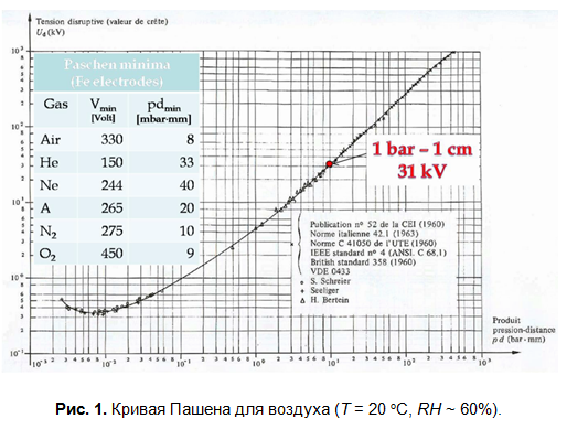
Any dielectric has electrical strength - at a certain intensity of the electric field there is a breakdown of it. In gases, the breakdown voltage of spherical electrodes at a given temperature and average values of pressure is described by Paschen’s law:

where p is the pressure, a and b are experimental constants depending on the gas. In fig. 1 shows the Paschen curve for dry air with a relative humidity of 60% at a temperature of 20 o C. Note that the Paschen curve has a minimum value. An increase in pressure leads to an increase in density and an increase in the probability of collisions, but reduces the mean free path and, consequently, the energy of the particles. This leads to an increase in the breakdown voltage in the high pressure region, on the right side of the graph. At low values, the breakdown mechanism depends on the ratio of the mean free path and the distance between the electrodes. The electrical strength of air at normal atmospheric pressure is 3.1 kV / mm and it decreases with increasing temperature and pressure drop. The value of 1-1.5 kV / mm is usually taken as a conservative estimate when designing electrical insulation.
')
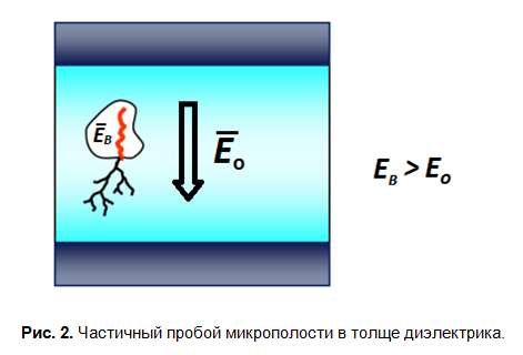
For solid dielectrics, the concept of intrinsic electric strength is introduced - the minimum value of the electric field strength in a homogeneous material, in which free or valence electrons acquire enough energy so that when they collide with atoms or bound electrons, new conduction electrons are formed, which leads to breakdown. This value depends on the temperature, for some materials it can reach several MV / mm and is the theoretical limit of the electric strength. In practice, breakdown occurs at much lower values of the electric field strength. The main reasons for this are:
The listed inhomogeneities in the bulk of the material act as concentrators of the electric field strength, leading to partial breakdowns (Fig. 2). As a result of such breakdowns, there is a gradual destruction of the material of the dielectric, which can lead to complete breakdown.
The presence of moisture or dirt on the surface can lead to the formation of conductive channels, which, even with low conductivity, create equipotential surfaces, reducing the actual gap between the electrodes and thereby leading to breakdown.
A whole complex of complex physical phenomena, including the probability component and depending on a large number of external factors, leads to electrical breakdown in dielectric materials. Therefore, analytical and computational models can be built only for the simplest cases. In practice, the design should be guided by the requirements of the standards, conduct insulation testing under conditions close to actual operating conditions, and, if possible, lay the insulation safety margin. Understanding the theoretical basis of electrical breakdown mechanisms allows you to make decisions in the context of the need to compromise with the recommendations of the standards.
Each group of electronic devices has its own electrical safety standard. The current security standard is 62368-1 , which replaced and merged the outdated standards 60950-1 and 60065. The standard, unlike its predecessors, is very systemic and structured and is recommended for study. Also, recommendations for galvanic isolation are specified in the IPC standards: in the general standard for the design of printed circuit boards IPC2221 and in the standard for voltage converters IPC9592.
The basic model of the protected system in 62368-1 looks very simple (Fig. 3). In the general case, mechanisms to protect against the transfer of energy (electrical, chemical, kinetic, heat, etc.) that can cause pain or cause injury include:
At the same time, protection in the standard means not only technical (including individual means of user protection), but also organizational measures. The highest priority from the point of view of safety are technical means that are part of the equipment, since they minimize the requirements for user behavior.

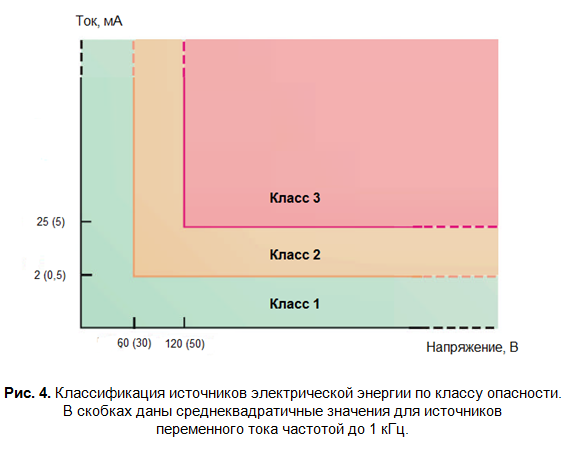
By hazard, energy sources are divided into three classes (section 4.2), each of which has its own minimum level of protection, depending on the type of equipment user. For a regular user, this is:
For sources of class 1, no protection is allowed. The standard requires protective insulation not only between the power source and the user, but also between sources of electrical energy of various hazard classes (standard table 12).
The classification of sources is devoted to section 5.2 of the standard. DC sources with an output voltage of more than 60 V are identified as dangerous and require isolation (Fig. 4). The same voltage levels are considered dangerous for single pulses and for capacitors with a capacity of more than 300 nF, while decreasing the capacity, requirements are reduced (for 4 nF it is already 1 kV, see table 7 of the standard). For AC sources, the threshold is 30 V rms voltage.
If electrical devices of class 2 and 3 are used in the operation of an electronic device, then when designing printed circuit boards that are part of it, the requirements for minimum clearances (clearance) and leakage paths (eng. Creepage), used materials and components should be observed. Printed circuit boards are devoted to a separate section G.18 of Appendix G “Components”, which contains links to general sections 5.4.2 “Clearances” and 5.4.3 “Leakage paths”.
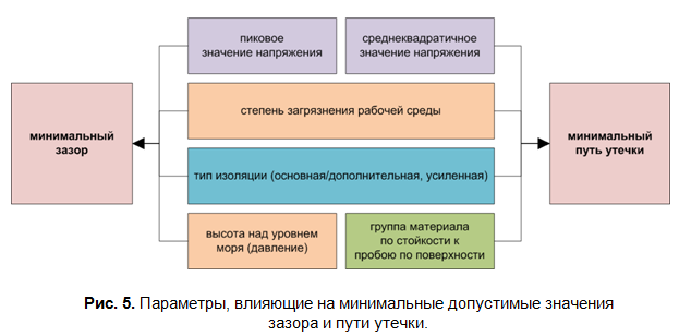
When choosing minimum clearances and creepage distances, one should proceed not only from the voltage values, but also from the operating conditions and the dielectric material (Fig. 5). Air gap breakdown is influenced by pressure, so the standard introduces multiplying factors for altitudes above 2000 m above sea level (standard table 22). In addition, three degrees of pollution of the working environment are determined. The higher the degree of contamination, the greater the distance between the conductors should be provided.
Another parameter that affects the value of the minimum creepage distance is the material group with respect to resistance to breakdown over the surface. The IEC 60112 standard divides dielectric materials into 4 groups depending on the value of the conventional CTI index (the Comparative Tracking Index). The higher the CTI value, the higher the resistance to breakdown and the smaller the values of the minimum creepage distance are permissible, ceteris paribus. The standard glass fiber laminate FR4 with CTI ~ 175 ... 200 is on the border of the values of group IIIb, which is not recommended for use with pollution degree 3 and with root-mean-square values of voltage more than 630 V.
After the parameters affecting the choice of minimum clearances and creepage distances are determined, the values themselves are determined using tables 17-19, 23, G.12 of the standard. These minimum distances must be maintained for all conductors if there is an appropriate voltage between them: in the primary circuit, between the primary and secondary circuits, as well as in the secondary circuits. Table 1 shows the minimum clearances and creepage distances for printed circuit boards that are part of devices powered by 220 V overvoltage category II under conditions of pollution degree 2.
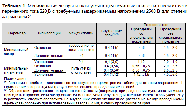
For the outer layers, the values depend on the presence of the coating; however, it should be borne in mind that the standard mask is not a specialized insulating coating and does not provide the possibility of applying reduced gaps requirements. The mask has an uneven thickness and may contain cavities and cracks, reducing the reliability of such insulation.
As for the inner layers, for conductors on adjacent layers, the minimum gap is used for solid (eng. Solid insulation) single-layer insulation of 0.4 mm, and for conductors on one layer, the insulation is considered as a bonded joint (eng. Cemented joint). According to the standard, the minimum clearances and creepage distances for pollution degree 2, for pollution degree 1 or a gap for solid insulation of 0.4 mm can be used for such insulation. At the same time, in the latter two cases, the standard requires tests, including thermal cycling and a test for electrical strength. The fact is that there is a probability (and for reliable applications it must be taken into account) that as a result of thermal, mechanical load or over time, along the section of adjacent layers of the printed circuit board, there will be a gap. And then a distance of 0.4 mm may not be sufficient to provide high-voltage insulation.
It is worth noting that in most cases the requirement for the distance through the insulation between the layers is minimal, so one of the strategies for designing printed circuit boards with a restriction on dimensions is to separate the insulated conductors and components into different layers.
Compliance with the required standard distances in the design of the topology of the printed circuit board may be insufficient, since the presence of components and structural elements of the product makes the task three-dimensional. Therefore, the use of 3D-models of components and the overall assembly of the product is a prerequisite for designing products with dangerous voltage levels.
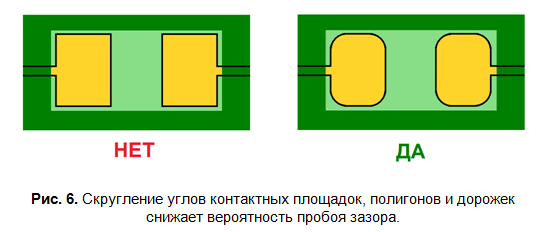
In addition to meeting the requirements for minimum distances, when designing printed circuit boards for high-voltage applications, it is recommended to avoid sharp corners in the geometry of conductive layers (Fig. 6), since they are concentrators of the electric field.
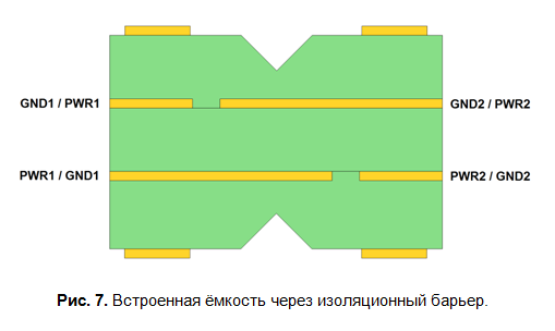
From the point of view of the EMC, the isolation barrier is a discontinuity in the return current path, which without special measures leads to an increased level of radiation, especially in the case of isolated power supplies. As in the case of breaks in the support layer, capacitors are used to ensure the flow path of the return currents through the insulation barrier. Requirements for discrete capacitors and examples of their application are described in Section G.15 of Appendix G “Components” of the standard. In insulation of hazardous voltage levels, only class Y capacitors are used, the failure of which leads to an open circuit: for 220 V AC mains, overvoltage class II is one capacitor of subclass Y1 or two series-connected capacitors of subclass Y2. The safety of such capacitors is guaranteed by the manufacturer, however, the parasitic inductance of the connection and the localized location limit their efficiency at frequencies above 100 MHz. This disadvantage is lacking the capacity built into the printed circuit board, distributed between two overlapping polygons on the inner layers (Fig. 7).
It is important to understand that even full adherence to the recommendations of the standard in terms of minimum distances between conductors does not guarantee electrical safety. Only the results of insulation resistance tests (section 5.4.11 of the standard) can confirm the compliance of the printed circuit board topology, the materials and components used, the product design and its manufacturing technology with the safety requirements for specific conditions of use.
Extended and more detailed versions of this and previous publications included in the new release of the full version of the book . The #SamsPcbGuide project is being developed, including through feedback (both positive and negative), so I will be grateful for constructive criticism. Good luck to everyone, people (and let safety not depend on luck, everything is strictly according to standards)!
Safety requirements apply to any electronic equipment, despite the fact that they are overhead from the point of view of the operation of the product. They require the use of additional circuit solutions and electronic components, complicate the topology of printed circuit boards, increasing the weight and dimensions of the product, the amount of testing and, thus, its cost and time to market. Only functionality can be limited only in the development of mock-ups or prototypes of the device. Unfortunately, at present, in terms of ease of access to the buyer (past certification centers), cost reduction and test savings, electronic products lose not only reliability but also safety.
Fundamentals of the theory of electrical breakdown in gases and solids
Any dielectric has electrical strength - at a certain intensity of the electric field there is a breakdown of it. In gases, the breakdown voltage of spherical electrodes at a given temperature and average values of pressure is described by Paschen’s law:
where p is the pressure, a and b are experimental constants depending on the gas. In fig. 1 shows the Paschen curve for dry air with a relative humidity of 60% at a temperature of 20 o C. Note that the Paschen curve has a minimum value. An increase in pressure leads to an increase in density and an increase in the probability of collisions, but reduces the mean free path and, consequently, the energy of the particles. This leads to an increase in the breakdown voltage in the high pressure region, on the right side of the graph. At low values, the breakdown mechanism depends on the ratio of the mean free path and the distance between the electrodes. The electrical strength of air at normal atmospheric pressure is 3.1 kV / mm and it decreases with increasing temperature and pressure drop. The value of 1-1.5 kV / mm is usually taken as a conservative estimate when designing electrical insulation.
')
For solid dielectrics, the concept of intrinsic electric strength is introduced - the minimum value of the electric field strength in a homogeneous material, in which free or valence electrons acquire enough energy so that when they collide with atoms or bound electrons, new conduction electrons are formed, which leads to breakdown. This value depends on the temperature, for some materials it can reach several MV / mm and is the theoretical limit of the electric strength. In practice, breakdown occurs at much lower values of the electric field strength. The main reasons for this are:
- heterogeneity of the material (mechanical microdamages, contamination and the cavity inside the material, damage to the atomic lattice when exposed to radiation, changes in properties as a result of chemical reactions);
- the presence of circumvention breakdown trajectories, most often along the boundary of the material (surface contamination, moisture on the surface and in the boundary layer), along the cracks;
- material aging with time - accumulation of the listed effects, including in conditions of elevated temperature.
The listed inhomogeneities in the bulk of the material act as concentrators of the electric field strength, leading to partial breakdowns (Fig. 2). As a result of such breakdowns, there is a gradual destruction of the material of the dielectric, which can lead to complete breakdown.
The presence of moisture or dirt on the surface can lead to the formation of conductive channels, which, even with low conductivity, create equipotential surfaces, reducing the actual gap between the electrodes and thereby leading to breakdown.
A whole complex of complex physical phenomena, including the probability component and depending on a large number of external factors, leads to electrical breakdown in dielectric materials. Therefore, analytical and computational models can be built only for the simplest cases. In practice, the design should be guided by the requirements of the standards, conduct insulation testing under conditions close to actual operating conditions, and, if possible, lay the insulation safety margin. Understanding the theoretical basis of electrical breakdown mechanisms allows you to make decisions in the context of the need to compromise with the recommendations of the standards.
New security standard
Each group of electronic devices has its own electrical safety standard. The current security standard is 62368-1 , which replaced and merged the outdated standards 60950-1 and 60065. The standard, unlike its predecessors, is very systemic and structured and is recommended for study. Also, recommendations for galvanic isolation are specified in the IPC standards: in the general standard for the design of printed circuit boards IPC2221 and in the standard for voltage converters IPC9592.
The basic model of the protected system in 62368-1 looks very simple (Fig. 3). In the general case, mechanisms to protect against the transfer of energy (electrical, chemical, kinetic, heat, etc.) that can cause pain or cause injury include:
- weakening the level or rate of energy transfer;
- energy redirection;
- power source shutdown;
- creating a barrier between the energy source and the user.
At the same time, protection in the standard means not only technical (including individual means of user protection), but also organizational measures. The highest priority from the point of view of safety are technical means that are part of the equipment, since they minimize the requirements for user behavior.
By hazard, energy sources are divided into three classes (section 4.2), each of which has its own minimum level of protection, depending on the type of equipment user. For a regular user, this is:
- basic protection (for hazard class 2) - ensures safety in normal and abnormal operating conditions,
- additional protection (for class 3) - is used in addition to the main one, providing protection against its malfunction,
- enhanced protection (for class 3) - ensures safety in normal and abnormal conditions of operation (for example, reverse polarity of the power supply), as well as in case of a single fault (for example, insulation breakdown).
For sources of class 1, no protection is allowed. The standard requires protective insulation not only between the power source and the user, but also between sources of electrical energy of various hazard classes (standard table 12).
The classification of sources is devoted to section 5.2 of the standard. DC sources with an output voltage of more than 60 V are identified as dangerous and require isolation (Fig. 4). The same voltage levels are considered dangerous for single pulses and for capacitors with a capacity of more than 300 nF, while decreasing the capacity, requirements are reduced (for 4 nF it is already 1 kV, see table 7 of the standard). For AC sources, the threshold is 30 V rms voltage.
If electrical devices of class 2 and 3 are used in the operation of an electronic device, then when designing printed circuit boards that are part of it, the requirements for minimum clearances (clearance) and leakage paths (eng. Creepage), used materials and components should be observed. Printed circuit boards are devoted to a separate section G.18 of Appendix G “Components”, which contains links to general sections 5.4.2 “Clearances” and 5.4.3 “Leakage paths”.
When choosing minimum clearances and creepage distances, one should proceed not only from the voltage values, but also from the operating conditions and the dielectric material (Fig. 5). Air gap breakdown is influenced by pressure, so the standard introduces multiplying factors for altitudes above 2000 m above sea level (standard table 22). In addition, three degrees of pollution of the working environment are determined. The higher the degree of contamination, the greater the distance between the conductors should be provided.
Another parameter that affects the value of the minimum creepage distance is the material group with respect to resistance to breakdown over the surface. The IEC 60112 standard divides dielectric materials into 4 groups depending on the value of the conventional CTI index (the Comparative Tracking Index). The higher the CTI value, the higher the resistance to breakdown and the smaller the values of the minimum creepage distance are permissible, ceteris paribus. The standard glass fiber laminate FR4 with CTI ~ 175 ... 200 is on the border of the values of group IIIb, which is not recommended for use with pollution degree 3 and with root-mean-square values of voltage more than 630 V.
After the parameters affecting the choice of minimum clearances and creepage distances are determined, the values themselves are determined using tables 17-19, 23, G.12 of the standard. These minimum distances must be maintained for all conductors if there is an appropriate voltage between them: in the primary circuit, between the primary and secondary circuits, as well as in the secondary circuits. Table 1 shows the minimum clearances and creepage distances for printed circuit boards that are part of devices powered by 220 V overvoltage category II under conditions of pollution degree 2.
For the outer layers, the values depend on the presence of the coating; however, it should be borne in mind that the standard mask is not a specialized insulating coating and does not provide the possibility of applying reduced gaps requirements. The mask has an uneven thickness and may contain cavities and cracks, reducing the reliability of such insulation.
As for the inner layers, for conductors on adjacent layers, the minimum gap is used for solid (eng. Solid insulation) single-layer insulation of 0.4 mm, and for conductors on one layer, the insulation is considered as a bonded joint (eng. Cemented joint). According to the standard, the minimum clearances and creepage distances for pollution degree 2, for pollution degree 1 or a gap for solid insulation of 0.4 mm can be used for such insulation. At the same time, in the latter two cases, the standard requires tests, including thermal cycling and a test for electrical strength. The fact is that there is a probability (and for reliable applications it must be taken into account) that as a result of thermal, mechanical load or over time, along the section of adjacent layers of the printed circuit board, there will be a gap. And then a distance of 0.4 mm may not be sufficient to provide high-voltage insulation.
It is worth noting that in most cases the requirement for the distance through the insulation between the layers is minimal, so one of the strategies for designing printed circuit boards with a restriction on dimensions is to separate the insulated conductors and components into different layers.
Compliance with the required standard distances in the design of the topology of the printed circuit board may be insufficient, since the presence of components and structural elements of the product makes the task three-dimensional. Therefore, the use of 3D-models of components and the overall assembly of the product is a prerequisite for designing products with dangerous voltage levels.
The minimum distances required by the standard must be maintained in all directions, taking into account the presence of components on the printed circuit board, as well as the structural elements of the product.
In addition to meeting the requirements for minimum distances, when designing printed circuit boards for high-voltage applications, it is recommended to avoid sharp corners in the geometry of conductive layers (Fig. 6), since they are concentrators of the electric field.
From the point of view of the EMC, the isolation barrier is a discontinuity in the return current path, which without special measures leads to an increased level of radiation, especially in the case of isolated power supplies. As in the case of breaks in the support layer, capacitors are used to ensure the flow path of the return currents through the insulation barrier. Requirements for discrete capacitors and examples of their application are described in Section G.15 of Appendix G “Components” of the standard. In insulation of hazardous voltage levels, only class Y capacitors are used, the failure of which leads to an open circuit: for 220 V AC mains, overvoltage class II is one capacitor of subclass Y1 or two series-connected capacitors of subclass Y2. The safety of such capacitors is guaranteed by the manufacturer, however, the parasitic inductance of the connection and the localized location limit their efficiency at frequencies above 100 MHz. This disadvantage is lacking the capacity built into the printed circuit board, distributed between two overlapping polygons on the inner layers (Fig. 7).
It is important to understand that even full adherence to the recommendations of the standard in terms of minimum distances between conductors does not guarantee electrical safety. Only the results of insulation resistance tests (section 5.4.11 of the standard) can confirm the compliance of the printed circuit board topology, the materials and components used, the product design and its manufacturing technology with the safety requirements for specific conditions of use.
Extended and more detailed versions of this and previous publications included in the new release of the full version of the book . The #SamsPcbGuide project is being developed, including through feedback (both positive and negative), so I will be grateful for constructive criticism. Good luck to everyone, people (and let safety not depend on luck, everything is strictly according to standards)!
Source: https://habr.com/ru/post/447944/
All Articles