Seven-segment display control using FPGA
Hi, Habr! I want to make my own contribution to the promotion of FPGA. In this article I will try to explain how to describe in VHDL language a device that controls a seven-segment display. But before starting, I want to briefly tell you how I came to FPGA and why I chose the VHDL language.
Somewhere half a year ago I decided to try my hand at programming FPGAs. Before this, I never encountered circuitry. There was little experience using microcontrollers (Atmega328p, STM32). Immediately after the decision to get comfortable with the FPGA, the question arose of choosing a language that I would use. The choice fell on VHDL because of its strong typing. As a beginner, I wanted to catch as many possible problems as possible at the synthesis stage, and not on the working device.
Why seven-segment display? Blinking LED already tired, and the logic of flashing them is not anything interesting. On the one hand, the control logic of the display is more complicated than LED blinking (that is, it is more interesting to write it), and on the other hand, it is rather simple to implement.
What I used in the process of creating a device:
')
Create a device that will show the numbers 0 - 9 in a cycle. Once a second, the value displayed on the display should increase by 1.
Implement this logic can be different. I will divide this device into modules, each of which will perform some action and the result of this action will be transferred to the next module.
The master device will control the correct transmission of signals between modules, as well as generate the rclk signal upon completion of the data transfer.
As can be seen from the diagram, the device has 1 incoming signal (clk) and 3 outgoing signals (sclk, dio, rclk). The clk signal comes in 2 signal dividers (sec_delay and transfer_delay). An outgoing signal with a period of 1 s leaves the sec_delay device. On the leading edge of this signal, the counter (bcd_counter1) starts to generate the next number to be displayed on the display. After the number is generated, the decoder (bcd_2_7seg1) converts the binary representation of the number into burning and non-burning segments on the display. Which, using the transmitter (transmitter1), are transmitted to the display. Transmitting clock is carried out using the device transfer_delay.
To create a device in VHDL, the construction of two components entity and architecture is used. The entity declares an interface for working with the device. Architecture describes the logic of the device.
Through the generic field, we can set the device to the desired delay. And in the ports field we describe incoming and outgoing signals from the device.
The code inside the process section is executed sequentially, any other code is executed in parallel. In parentheses, after the process keyword, there are signals that, if they are changed, this process will be launched (sensivity list).
The bcd_counter device in terms of execution logic is identical to the delay device. Therefore, I will not dwell on it in detail.
All the logic of this device is executed in parallel. I told about how to get the formulas for this device in one of the videos on my channel. Who cares, here's a link to the video .
I redirect to the sclk signal the value of the clk signal entering the transmitter, but only if the device is currently transmitting data (ready signal = false). Otherwise, the value of the sclk signal will be 0. At the beginning of the data transfer (signal enable = true), I combine the data from the two 8-bit vectors (digit_pos and digit) in the device into the 16-bit vector (data_v) and transmit the data from this vector is one bit per clock, setting the value of the transmitted bit to the outgoing signal dio. Of the interesting things in this device, I want to note that the data in dio are set on the falling edge of the clk signal, and the data from the pin dio will be recorded in the shift register of the display by the arrival of the leading edge of the sclk signal. Upon completion of the transmission, setting the signal ready <= true I signal to other devices that the transmission was completed.
This device controls other devices. Here, before declaring auxiliary signals, I declare the components that I will use. In the architecture itself (after the begin keyword) I create device instances:
After instances of components, a process is declared. This process solves several problems:
First, the data “10011111“ is transmitted. Then the position of the number is transmitted on the display “00010000“ (this parameter comes to the transmitter as a constant X "10"). In both cases, the rightmost bit (lsb) is transmitted first.
All code can be viewed on github . Files with postscript * _tb.vhd are debugging files for the respective components (for example, transmitter_tb.vhd is a debugging file for the transmitter). I just filled them up on github just in case. This code was downloaded and worked on a real board. Who cares, an illustration of the code can be viewed here (from 15:30). Thanks for attention.
Somewhere half a year ago I decided to try my hand at programming FPGAs. Before this, I never encountered circuitry. There was little experience using microcontrollers (Atmega328p, STM32). Immediately after the decision to get comfortable with the FPGA, the question arose of choosing a language that I would use. The choice fell on VHDL because of its strong typing. As a beginner, I wanted to catch as many possible problems as possible at the synthesis stage, and not on the working device.
Why seven-segment display? Blinking LED already tired, and the logic of flashing them is not anything interesting. On the one hand, the control logic of the display is more complicated than LED blinking (that is, it is more interesting to write it), and on the other hand, it is rather simple to implement.
What I used in the process of creating a device:
')
- FPGA Altera Cyclone II (I know that it is hopelessly outdated, but you can buy it from the Chinese for a penny)
- Quartus II version 13.0.0 (as far as I know this is the latest version supporting Cyclone II)
- Simulator ModelSim
- Seven-segment shift register display
Task
Create a device that will show the numbers 0 - 9 in a cycle. Once a second, the value displayed on the display should increase by 1.
Implement this logic can be different. I will divide this device into modules, each of which will perform some action and the result of this action will be transferred to the next module.
Modules
- This device should be able to count time. To calculate the time, I created the module "delay". This module has 1 incoming and 1 outgoing signal. The module receives the FPGA frequency signal and, after a specified number of periods of the incoming signal, changes the value of the outgoing signal to the opposite.
- The device should count from 0 to 9. This will use the bcd_counter module.
- In order to light a segment on the display, you need to set the corresponding bit segment to 0 in the shift register of the display, and in order to cancel the segment you need to write 1 in bits (my display has inverted logic). The bcd_2_7seg decoder will be engaged in setting and resetting the necessary bits.
- The transmitter module will be responsible for data transmission.
The master device will control the correct transmission of signals between modules, as well as generate the rclk signal upon completion of the data transfer.
For clarity, I present the scheme of this device.
As can be seen from the diagram, the device has 1 incoming signal (clk) and 3 outgoing signals (sclk, dio, rclk). The clk signal comes in 2 signal dividers (sec_delay and transfer_delay). An outgoing signal with a period of 1 s leaves the sec_delay device. On the leading edge of this signal, the counter (bcd_counter1) starts to generate the next number to be displayed on the display. After the number is generated, the decoder (bcd_2_7seg1) converts the binary representation of the number into burning and non-burning segments on the display. Which, using the transmitter (transmitter1), are transmitted to the display. Transmitting clock is carried out using the device transfer_delay.
Code
To create a device in VHDL, the construction of two components entity and architecture is used. The entity declares an interface for working with the device. Architecture describes the logic of the device.
Here's what the entity delay device looks like.
entity delay is -- entity, generic generic (delay_cnt: integer); -- port(clk: in std_logic; out_s: out std_logic := '0'); end entity delay; Through the generic field, we can set the device to the desired delay. And in the ports field we describe incoming and outgoing signals from the device.
The architecture of the delay device is as follows.
-- architecture , -- entity 0 architecture delay_arch of delay is begin delay_proc: process(clk) variable clk_cnt: integer range 0 to delay_cnt := 0; variable out_v: std_logic := '0'; begin -- if(rising_edge(clk)) then clk_cnt := clk_cnt + 1; if(clk_cnt >= delay_cnt) then -- switch/case VHDL case out_v is when '0' => out_v := '1'; when others => out_v := '0'; end case; clk_cnt := 0; -- out_s out_v out_s <= out_v; end if; end if; end process delay_proc; end delay_arch; The code inside the process section is executed sequentially, any other code is executed in parallel. In parentheses, after the process keyword, there are signals that, if they are changed, this process will be launched (sensivity list).
The bcd_counter device in terms of execution logic is identical to the delay device. Therefore, I will not dwell on it in detail.
Here's what the entity and architecture decoder looks like.
entity bcd_to_7seg is port(bcd: in std_logic_vector(3 downto 0) := X"0"; disp_out: out std_logic_vector(7 downto 0) := X"00"); end entity bcd_to_7seg; architecture bcd_to_7seg_arch of bcd_to_7seg is signal not_bcd_s: std_logic_vector(3 downto 0) := X"0"; begin not_bcd_s <= not bcd; disp_out(7) <= (bcd(2) and not_bcd_s(1) and not_bcd_s(0)) or (not_bcd_s(3) and not_bcd_s(2) and not_bcd_s(1) and bcd(0)); disp_out(6) <= (bcd(2) and not_bcd_s(1) and bcd(0)) or (bcd(2) and bcd(1) and not_bcd_s(0)); disp_out(5) <= not_bcd_s(2) and bcd(1) and not_bcd_s(0); disp_out(4) <= (not_bcd_s(3) and not_bcd_s(2) and not_bcd_s(1) and bcd(0)) or (bcd(2) and not_bcd_s(1) and not_bcd_s(0)) or (bcd(2) and bcd(1) and bcd(0)); disp_out(3) <= (bcd(2) and not_bcd_s(1)) or bcd(0); disp_out(2) <= (not_bcd_s(3) and not_bcd_s(2) and bcd(0)) or (not_bcd_s(3) and not_bcd_s(2) and bcd(1)) or (bcd(1) and bcd(0)); disp_out(1) <= (not_bcd_s(3) and not_bcd_s(2) and not_bcd_s(1)) or (bcd(2) and bcd(1) and bcd(0)); disp_out(0) <= '1'; end bcd_to_7seg_arch; All the logic of this device is executed in parallel. I told about how to get the formulas for this device in one of the videos on my channel. Who cares, here's a link to the video .
In the transmitter, I combine sequential and parallel logic
entity transmitter is port(enable: in boolean; clk: in std_logic; digit_pos: in std_logic_vector(7 downto 0) := X"00"; digit: in std_logic_vector(7 downto 0) := X"00"; sclk, dio: out std_logic := '0'; ready: buffer boolean := true); end entity transmitter; architecture transmitter_arch of transmitter is constant max_int: integer := 16; begin sclk <= clk when not ready else '0'; send_proc: process(clk, enable, ready) variable dio_cnt_v: integer range 0 to max_int := 0; variable data_v: std_logic_vector((max_int - 1) downto 0); begin -- dio clk if(falling_edge(clk) and (enable or not ready)) then if(dio_cnt_v = 0) then -- , -- data_v := digit_pos & digit; ready <= false; end if; if(dio_cnt_v = max_int) then dio_cnt_v := 0; ready <= true; dio <= '0'; else dio <= data_v(dio_cnt_v); dio_cnt_v := dio_cnt_v + 1; end if; end if; end process send_proc; end transmitter_arch; I redirect to the sclk signal the value of the clk signal entering the transmitter, but only if the device is currently transmitting data (ready signal = false). Otherwise, the value of the sclk signal will be 0. At the beginning of the data transfer (signal enable = true), I combine the data from the two 8-bit vectors (digit_pos and digit) in the device into the 16-bit vector (data_v) and transmit the data from this vector is one bit per clock, setting the value of the transmitted bit to the outgoing signal dio. Of the interesting things in this device, I want to note that the data in dio are set on the falling edge of the clk signal, and the data from the pin dio will be recorded in the shift register of the display by the arrival of the leading edge of the sclk signal. Upon completion of the transmission, setting the signal ready <= true I signal to other devices that the transmission was completed.
Here is what the entity and architecture of the display device looks like.
entity display is port(clk: in std_logic; sclk, rclk, dio: out std_logic := '0'); end entity display; architecture display_arch of display is component delay is generic (delay_cnt: integer); port(clk: in std_logic; out_s: out std_logic := '0'); end component; component bcd_counter is port(clk: in std_logic; bcd: out std_logic_vector(3 downto 0)); end component; component bcd_to_7seg is port(bcd: in std_logic_vector(3 downto 0); disp_out: out std_logic_vector(7 downto 0)); end component; component transmitter is port(enable: in boolean; clk: in std_logic; digit_pos: in std_logic_vector(7 downto 0); digit: in std_logic_vector(7 downto 0); sclk, dio: out std_logic; ready: buffer boolean); end component; signal sec_s: std_logic := '0'; signal bcd_counter_s: std_logic_vector(3 downto 0) := X"0"; signal disp_out_s: std_logic_vector(7 downto 0) := X"00"; signal tr_enable_s: boolean; signal tr_ready_s: boolean; signal tr_data_s: std_logic_vector(7 downto 0) := X"00"; -- , tr_ready_s -- rclk signal disp_refresh_s: boolean; signal transfer_clk: std_logic := '0'; begin sec_delay: delay generic map(25_000_000) port map(clk, sec_s); transfer_delay: delay generic map(10) port map(clk, transfer_clk); bcd_counter1: bcd_counter port map(sec_s, bcd_counter_s); bcd_to_7seg1: bcd_to_7seg port map(bcd_counter_s, disp_out_s); transmitter1: transmitter port map(tr_enable_s, transfer_clk, X"10", tr_data_s, sclk, dio, tr_ready_s); tr_proc: process(transfer_clk) variable prev_disp: std_logic_vector(7 downto 0); variable rclk_v: std_logic := '0'; begin if(rising_edge(transfer_clk)) then -- if(tr_ready_s) then -- if(not (prev_disp = disp_out_s)) then prev_disp := disp_out_s; -- tr_data_s <= disp_out_s; -- tr_enable_s <= true; end if; else disp_refresh_s <= true; -- -- , -- tr_enable_s <= false; end if; if(rclk_v = '1') then disp_refresh_s <= false; end if; if(tr_ready_s and disp_refresh_s) then rclk_v := '1'; else rclk_v := '0'; end if; rclk <= rclk_v; end if; end process tr_proc; end display_arch; This device controls other devices. Here, before declaring auxiliary signals, I declare the components that I will use. In the architecture itself (after the begin keyword) I create device instances:
- sec_delay is an instance of the delay component. The outgoing signal is sent to the signal sec_s.
- transfer_delay is an instance of the delay component. The outgoing signal is sent to the transfer_clk signal.
- bcd_counter1 is an instance of the bcd_counter component. The outgoing signal is sent to the bcd_counter_s signal.
- bcd_to_7seg1 is an instance of the bcd_to_7seg component. The outgoing signal is sent to the disp_out_s signal.
- transmitter1 is an instance of the transmitter component. Outgoing signals are sent to the signals sclk, dio, tr_ready_s.
After instances of components, a process is declared. This process solves several problems:
- If the transmitter is not busy, the process initializes the start of data transfer.
if(tr_ready_s) then if(not (prev_disp = disp_out_s)) then prev_disp := disp_out_s; -- -- tr_data_s <= disp_out_s; -- tr_enable_s <= true; end if; else ... - If the transmitter is busy (tr_ready_s = false), then the process sets the value of the signal disp_refresh_s <= true (this signal means that you need to update the data on the display after the transfer is completed). The value of the signal tr_enable_s <= false is also set; if this is not done before the completion of the transmission, then the data loaded into the transmitter will be re-transmitted
- Sets and resets the rclk signal when data transfer is complete.
if(rclk_v = '1') then disp_refresh_s <= false; end if; if(tr_ready_s and disp_refresh_s) then rclk_v := '1'; else rclk_v := '0'; end if; rclk <= rclk_v;
Timing chart
Here is the time diagram of the transfer of the number 1 to the first position of the display.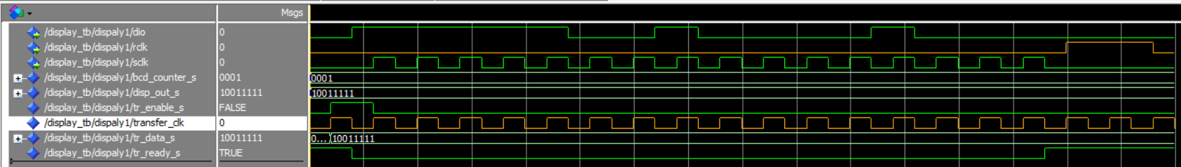
First, the data “10011111“ is transmitted. Then the position of the number is transmitted on the display “00010000“ (this parameter comes to the transmitter as a constant X "10"). In both cases, the rightmost bit (lsb) is transmitted first.
All code can be viewed on github . Files with postscript * _tb.vhd are debugging files for the respective components (for example, transmitter_tb.vhd is a debugging file for the transmitter). I just filled them up on github just in case. This code was downloaded and worked on a real board. Who cares, an illustration of the code can be viewed here (from 15:30). Thanks for attention.
Source: https://habr.com/ru/post/447454/
All Articles