How does the computer inside the Hayabusy-2, which dropped a bomb on Ryuga. And photos of its developers
In this post I will briefly describe what is included in the So5 HR5000 and its processor core, show photos of two of the key developers of the MIPS 4K and 5K lines, and also tell how you can play at home on the FPGA board with the “descendant of the younger brother” of this computer The 32-bit MIPS microAptiv UP kernel, whose Verilog hardware description code was based on MIPS 4KEc.

Japan Aerospace Agency JAXA licensed processor core MIPS 5Kf from the US company MIPS Technologies. This happened back in the 2000s. The group that developed this core has existed in different configurations for 40 years:
')
- First, in 1978-1984, MIPS was a project in Stanford, under the direction of John Hennessy. On the success of this project, Hennessy became the author of the most famous textbook on computer architecture and at some point the president of Stanford.
- Then, in 1984, MIPS became a commercial company - MIPS Computer Systems. In the same year, ARM was commercialized. In 1991, MIPS released the world's first 64-bit microprocessor - MIPS R4000.
- After that, MIPS was absorbed by Silicon Graphics and in the 1990s was used inside graphic stations, where the first films with realistic graphics were made in Hollywood (“Jurassic Park”).
- In the 2000s, the group emerged in the company MIPS Technologies and in particular designed a processor for JAXA. The headquarters of MIPS was located in California, some of the developers of MIPS 5Kf sat in the European branch of MIPS in Copenhagen.
- In 2012, MIPS Technologies bought the British company Imagination Technologies, which became famous as a GPU developer inside the early Apple iPhone.
- In 2017, Apple threw Imagination and, after some perturbations, technology and part of the MIPS group were integrated into Wave Computing, a startup that develops a chip to accelerate neural networks.
- Wave Computing Chip is a combination of a cluster of 64-bit MIPS I6500 processors, a matrix multiplier based on the systolic array a la Google TPU, and a dataflow processor based on a Coarse-Grained Reconfigurable Architecture (CGRA) device. ). Classical processors in the I6500 cluster load the matrix multiplier and data stream processor, the matrix multiplier provides computational density, and the task stream processor is halfway between the classic processor and the matrix multiplier — it is more flexible than the multiplier and more productive than the classic CPU.
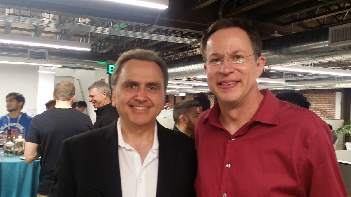
So I took a picture with one of the two key developers of the MIPS 4K and 5K line - Larry Hudepohl, Larry Hudepol (in the red shirt on the right). Larry began his career at Digital Equipment Corporation (DEC) as a processor designer for MicroVAX. Then Larry worked in a small company Cyrix, which in the late 1980s defied Intel and made an FPU coprocessor that was compatible with Intel 80387 and was 50% faster than it. Then Larry designed the MIPS chips in Silicon Graphics. When MIPS Technologies separated from Silicon Graphics, Larry and Ryan Kinter together started the first independent MIPS product - MIPS 4K, which became the basis of the line that dominates the 2000s home electronics (DVD players, cameras, digital TVs). Then MIPS 5K flew into space - it was used by the Japanese space agency JAXA. Then Larry in the position of VP Hardware Engineering led the development of the following lines, and is now working on new Wave Accelerator architectures:
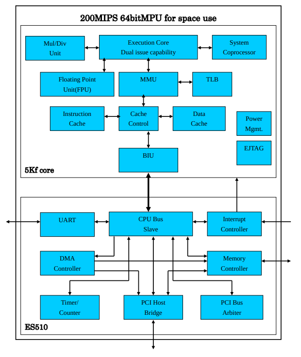
Now back to the processor in Hayabus-2 (in Hayabus-1, it is different). Here is the datasheet on the MIPS64 5Kf processor core and the HR5000 system data page . Note some interesting points.
First of all, MIPS 5Kf is a pipeline processor. If you are unfamiliar with how it works, then the easiest way to get acquainted is to study the seventh chapter of the book “Digital circuit design and computer architecture” by David M. Harris and Sarah L. Harris, the latest version of which can be downloaded here or here . At the same time, the conveyor in MIPS 5Kf is different from the classic MIPS conveyor from Harris & Harris. Those of you who read X & X can look at the differences and guess why:
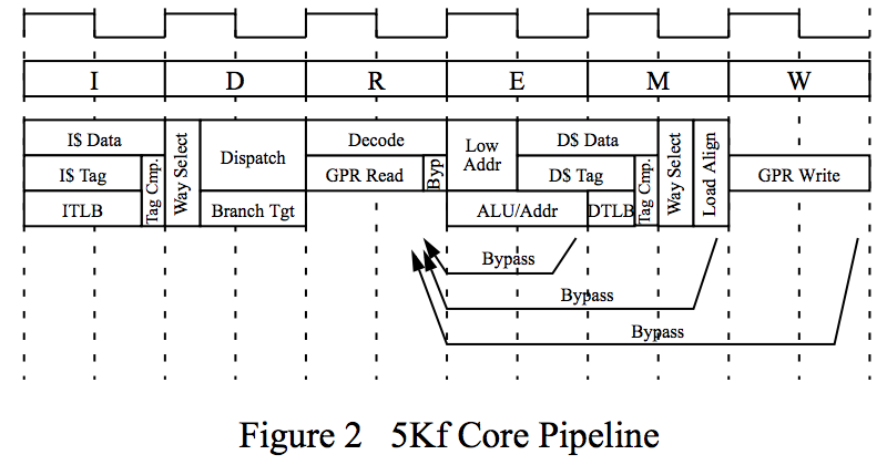
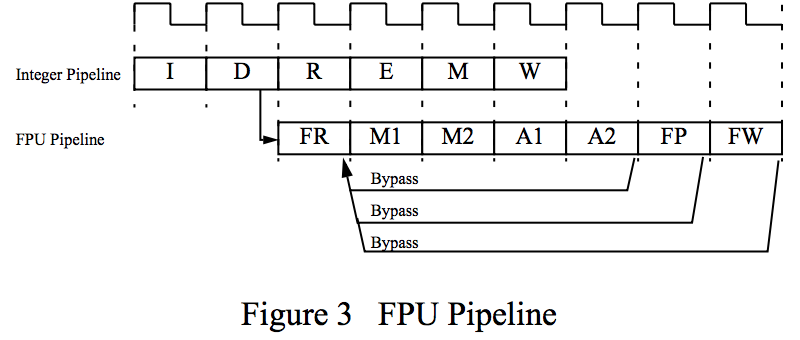
Of course, the MIPS 5Kf does not have five pipeline stages, but six, with the additional Dispatch stage. This stage is needed to make MIPS 5Kf limited-superscalar. It can perform not only one-by-one operations in the pipeline, but also can perform a floating-point operation simultaneously with an integer operation or with a memory operation (load or save). The Dispatch stage runs a floating point coprocessor that has its own seven-stage pipeline:
But on the right of the photo is Darren Jones, Darren Jones, the FPU developer at MIPS 5Kf. The letter “f” in “5Kf” means exactly that it has a floating point:

Here in this plate you can see how many cycles require different operations in the FPU and how often (repeat rate) they can be run into the pipeline. For example, multiplication of single precision requires four cycles, but you can run a new multiplication into the pipeline each cycle. So the FPU can simultaneously process four single precision multiplications at each stage of processing. But the multiplication of double precision requires five cycles, and it can be started only with a pause in the cycle. A complex double-square root operation requires as many as 32 cycles, and a new square-root can only be launched after 29 cycles. This is how the calculation of the coordinates of the ship and the formulas for its movement in outer space is optimized:

Hayabusa-2 uses the MIPS 5Kf configuration with separate 32-kilobyte instruction and data caches. At the same time, it is not clear from the brief description of the HR5000 whether it uses a four-channel cache of 8 kilobytes each - or a dual-channel cache of 16 kilobytes each. You can read how these caches work in X & X, as well as in my old caching presentation , as well as in the See MIPS Run Linux 2nd Edition by Dominic Sweetman useful book :

The Hayabus-2 also has a Memory Management Unit (MMU), with a Translation Lookaside Buffer (TLB) buffer. TLB is a universal tool for quickly converting addresses from virtual to physical. TLB allows you to:
Hide the operating system memory from unprivileged code.
Protect user programs from each other.
Provide program access to the amount of virtual memory that exceeds the amount of physical RAM.
Address more physical memory than available virtual addresses.
Place the program in any part of the physical memory.
Allows multiple regions of memory to look like a sequential piece.
Allows you to load pieces of the program from an external device as needed.
TLB also associates with the address various attributes: the prohibition of reading, writing and execution, as well as the attributes of cacheability and coherence.
The cacheability attribute is needed to show the processor where the address space is for the next level of the cache, and where it is for the I / O solvers that cannot be cached.
Attributes of coherence are needed for joint work of several processor cores, each of which has its own first-level cache, and together they use a common second-level cache.
TLB can store an indicator that a record has been recorded on the page with this address. This helps when swapping, loading and unloading memory pages on systems with less physical memory than the application needs to address all pieces of their code and data with virtual addresses.
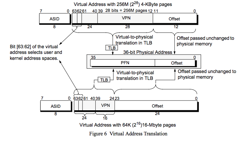
Here is the translation of a 64-bit virtual address into a 36-bit physical address on MIPS 5Kf. Why on Hayabus-2 64-bit processor with 36-bit physical addresses? I suspect that Hayabusa-2 takes photographs and must process images, for which it takes a lot of memory. Perhaps for some algorithms, 64-bit arithmetic and 64-bit exchanges with a cache (or 64-bit non-cached exchanges with memory) improve something, and it turns out to be useful in space. But I don’t know for sure, you probably need to ask Zelenyikot and amartology , who know more about space than I do.
You can read about TLB in X & X and See MIPS Run, but there is a nuance: both books describe what TLB looks like from a programmer's point of view. But from the point of view of the hardware developer, the CPU designers are deceiving the programmer, showing him TLB as one associative translation table, while there are actually three tables inside the TLB Hayabusy-2: micro-TLB instructions, micro-TLB data and common (Joint TLB). First, the memory management device searches in ITLB and DTLB, and only if it does not find it, takes it from JTLB. It costs the processor extra 2 cycles. Also see my old TLB presentation :

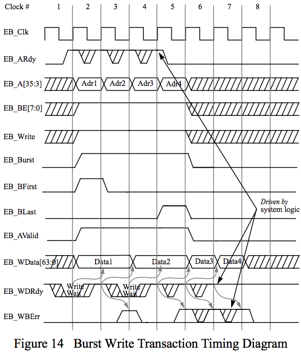
The interface between the first-level caches and the memory controller in MIPS 5Kf in Hayabusa-2 is called EB (pronounced IB). This is short for External Bus. It is similar to AHB and AXI, and allows you to make a burst, get a whole line from the cache or fill the cache with memory, using transfers in successive cycles.

Outside the processor core, the HR5000 has an interrupt controller, a UART module, a direct memory access controller, timers, and a PCI controller:
To work in space, the chip must be protected from radiation. I am not an expert in radiation protection, for this there is amartology on Habré, but I know that such protection can be done both at the level of physical production technology, and at the level of various ECC checks, and even at the level of architecture, with triplication, etc. The creators of the HR5000 on-chip system decided to use the usual RTL2GDSII route adopted in commercial applications, the synthesis of a graph from logical elements from the code in the Verilog hardware description language. However, after receiving such a graph (netlist), they modify it with the help of a special hardness-by-design (HBD) primitive library (never used this, so any explanation in the comments is welcome):

Since MIPS 5Kf is written in Verilog, it can be turned not only into a netlist, and not only into a mask for the production of a chip at a factory, but also into a FPGA configuration. Unfortunately, the MIPS 5Kf sources are not in open access, but in open access are the sources of a descendant of its “younger brother”, a 32-bit MIPS 4K processor. This “descendant” is called MIPS microAptiv UP, and its basic configuration is included in the MIPSfpga package. The MIPS 4K / 4KEc / microAptiv UP / M5150 code (these are all progressive versions of the line) was also written by Larry, Ryan and Darren.
You can play with the pipeline, caches, memory management device and interrupt the kernel MIPS microAptiv UP, run it on the simulator or the board with FPGA / FPGA. To do this, just download the MIPS Open ™ FPGA Getting Started Package , along with MIPS Open ™ FPGA Labs , and (this is important!) Add it to the MIPSfpga + . In the latter there are labs about the pipeline, cache and memory management device .
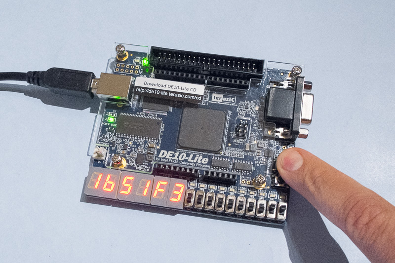
You can synthesize and run a MIPS microAptiv UP processor on a low-cost $ 85 motherboard (academic price is $ 55):
To work with the MIPSfpga / MIPSfpga + package, you need knowledge of the Verilog hardware description language, design principles at the register transfer level, and the ability to write in MIPS assembler.
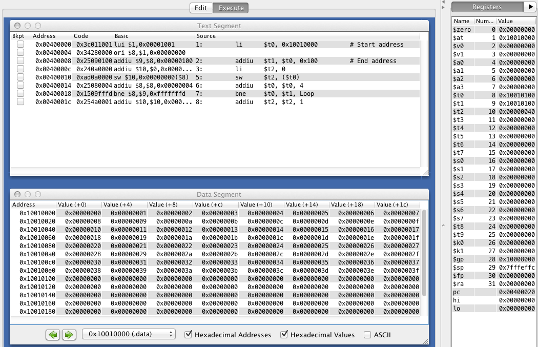
MIPS assembler is the easiest to learn. For this you can download the MARS simulator (MIPS Assembler and Runtime Simulator) . You can learn to use it in 5 minutes, in fact there are three buttons in it - to assemble, run, run in steps:
Then you can spend the day practicing writing in assembly language from Harris & Harris and See MIPS Run Linux books.
If you do not know anything at all about the development of digital circuits in general and in the hardware description language in particular, you can start with the Rosnan online course for schoolchildren, in three parts: “From the transistor to a chip” , “The logical side of digital circuitry” , “The physical side digital circuitry " ). Then you can study Verilog on X & X and understand that there is a processor using a simplified processor schoolMIPS .
If you are interested in this topic and want to participate in the work on the MIPS Open (as part of which the core of MIPS microAptiv UP was open), write in the comments. Rosnanovtsy also conduct a seminar for schoolchildren on digital design on April 17-19 , which will also include this space processor. Hayabusa-2 bombarded Ryugu for good reason - this is also an occasion for Russian schoolchildren and students to find out what is inside her.
Source: https://habr.com/ru/post/447324/
All Articles