Maximum direct current through field effect transistor
On the Internet, there is a lot of information about field-effect transistors (hereinafter referred to as PT) and their parameters, but one of the fairly simple at first glance parameters, namely, the maximum direct current that the transistor can pass through itself in the key mode, and not burn given in datasheets is somehow blurry and unobvious.
The article will consider an example of calculating the maximum current through the MOSFET SQM50P03-07 (took the first one from its scheme), operating in the key mode, or in the saturation section.
First, a little theory to understand what is the essence of the problem. Who just needs to calculate the current - go straight to the practice.
In short, the main parameter that limits the maximum current through the PT is the temperature, or rather its growth. Even when operating in the key mode, when the current flows through the source-drain, the transistor has some resistance, for powerful MOSFET this value can be only a few mW (not the biggest and not the smallest value among PTs). When current passes through such a resistance, some power is dissipated on it (transforming into heat, the transistor heats up). The dissipated power is directly proportional to the square of the current passing through the PT.
')
The problem is that the maximum current (DC), like the maximum power dissipation, is often not indicated directly in the documentation, for example, the datasheet screen on SQM50P03-07:
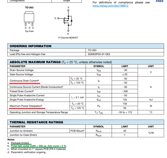
Continuous Drain Current is 50 amps, but with a footnote that this is a limitation of the case, i.e. a current greater than this cannot physically pass through the body itself without destroying the structure.
Maximum Power Dissipation for different temperatures of 150 and 50 W, but with a footnote that this is when current is passed by pulses, where for 1 period 98% of the time the transistor is “turned off” and the remaining 2% is “on” (remember, we are interested in direct current) .
So, to calculate the maximum current through the PT, an important parameter here is the maximum temperature. From the datasheet it is clear that it is 175 ° C ( Operating Junction and Storage Temperature Range ), and it is necessary to make a start from it in calculations. It is necessary to determine which current will heat the semiconductor channel of the transistor to 175 ° C, but a further increase in temperature will not occur due to the transfer of heat to the environment (cooling), this will be the current value that we need.
Heating a transistor, like any other body, is a complex process and depends on many parameters. In order to maximally simplify the actions connected with thermal calculations, the thermal resistance parameter is introduced, i.e. the ability of something to prevent the spread of heat. The greater the thermal resistance, the slower the PT will cool, and the faster the temperature of its crystal will rise to a critical one. Also, the greater the difference between the maximum allowable temperature on the chip and the environment, the longer the PT will heat up, and the more current it will be possible to pass through it.
Each material has its own thermal resistance, and the transistor, in turn, consists of a substrate (body) on which a conductive channel is formed, an insulator, the body itself, which may also consist of several materials, of course they are also of different thickness, which affects heat transfer.
In addition, the transistor can also be cooled in different ways, on some, there is a large contact pad that is soldered to the board or attached to the radiator, in such cases the thermal resistance is minimal. Some transistors do not have such sites and are in contact with the environment only through a plastic case, through which heat is released much more slowly.
The result is approximately the following scheme:
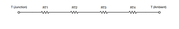
Where
With thermal resistance, as in electrical engineering, the rule works: “total resistance is equal to the sum of series resistances”.
As noted earlier, the PT can be cooled in different ways, and it is simply impossible to foresee all possible options in the datasheet, however, the most common ones are usually given:
Thermal resistances are not always indicated directly on the page with the maximum PT parameters, for example, a screen from the Si4477DY documentation:
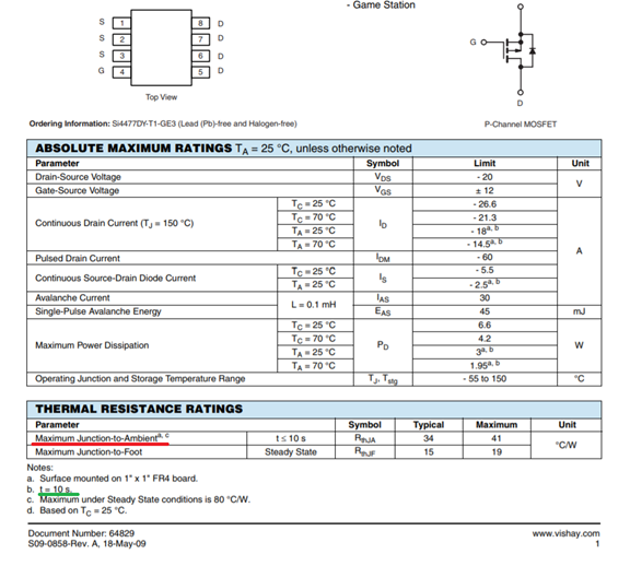
Although there is a Junction-to-Foot parameter, suppose we are interested in precisely the thermal resistance of Junction-to-Ambient , and it is given only for a time less than 10 seconds. In this case, you can rummage on the manufacturer's website and find models of thermal resistance. In such documents there is a graph of the dependence of the temperature difference Junction-Ambient on time:
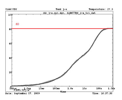
The graph shows that after 1000 seconds, a significant increase in temperature change stops. In this mode, the temperature difference is numerically equal to the thermal resistance. Therefore, for direct current, you can focus on the value of 80 ° C / W - the thermal resistance of Junction-to-Ambient .
(a little more in the comments )
Maybe not all companies have this information, but all of them are mostly standard PT hulls, it is enough to find the resistance data for another hull of interest to us.
When the developer has determined how exactly the PT will cool, the ambient temperature in which the device will operate, after that, you can finally proceed to the calculation.
Consider an example of determining the maximum direct current through the MOSFET SQM50P03-07 in the key mode, which is soldered to a 300x300 mm board (without a radiator). The board will work in the air at a maximum temperature of 45 ° C. We will control the PT by applying a voltage of 5 volts to its gate.
MOSFET is heated in the area of the formed conductive channel (on the substrate under the insulator and gate), this is the temperature Tjunction (temperature at the junction). From the datasheet of the Operating Junction and Storage Temperature Range -55 ... +175 , since we are interested in the maximum current, then we take the maximum temperature, i.e. TJMAX = 175 ° C (if you don’t want the transistor channel to be so hot, you can take a lower value).
Ambient temperature We take the maximum possible temperature to which the transistor will have to give off heat, according to the initial conditions TA = 45 ° C.
In the datasheet we find the thermal resistance of the conductive channel of the transistor to the environment, moreover, below there is a note that this resistance is relevant if the PT is soldered to a board larger than 1 inch square (in this case, some of the heat goes to the board, and with such dimensions, the necessary heat sink is carried out):
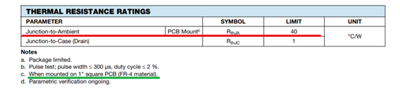
Thus, RΘJA = 40 ° C / W.
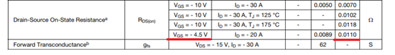
Maximum drain-source resistance at a certain control voltage at the gate. Information can be taken from the table, but the values of the channel resistance are given there only at gate voltages of 10V and 4.5V, while our plan is 5 volts. The difference, of course, is small, you can take 4.5V:
It’s better to find in the datasheet the dependence of the channel resistance on the voltage applied to the gate:
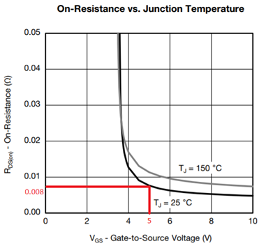
It is necessary to pay attention to the fact that in the case of the table, the data are given for TC = 25 ° C (substrate temperature), and in the case of the schedule there are 2 options: TJ = 25 ° C and TJ = 150 ° C (channel temperature). In the selected example, the channel will warm up to 175 ° C (as determined in the first calculation point). It turns out that at the moment it is better to use not the table, but the graph, to determine the channel resistance, since The value given in the table at TC = 25 ° C is not what we are interested in right now.
So, 8 mOhm (0.008 Ohm) is the resistance of the channel at its temperature of 25 ° C. To determine the resistance at a temperature TJMAX = 175 ° C, we look for a graph of the dependence of the normalized channel resistance on its temperature:

The horizontal axis is the connection temperature, and the vertical increment coefficient to the resistance. It can be noted that at 25 ° C it is equal to 1 (dimensionless value), i.e. the value that was previously determined (8 mΩ) is at this level. At a temperature of 175 ° C, the coefficient is about 1.69 .
To find the channel resistance at TJ = 175 ° C , multiply the resistance at 25 ° C by the coefficient at 175 ° C. We get 0.008 * 1.69 = 13.52 mΩ. RDS (ON) = 13.52 mΩ (0.013352 Ω) .
Now you can use the formula below to determine the maximum current (DC) that the transistor can skip:
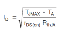
We get 15,504 amps.
However, calculations using thermal models based on thermal resistances have an error that occurs due to the simplification of those same models. Therefore, it is recommended to make a current margin of at least 20% . We make the last calculation and get 12,403 amps . This is the current value that SQM50P03-07 can pass through itself in the saturation mode and not burn, at the initial conditions specified above.
Note how the value of 12 A differs from what is indicated on the first pages of the datasheet (50 A, 150 A), such figures are confusing at first, if you do not deal with all the nuances.
In conclusion, a few words about the Safe Operating Area , this is a diagram showing the areas of normal operation of the transistor in different modes. For the same SQM50P03-07 there is an SOA in the datasheet, however, as you can see, it is given for a channel temperature of 25 ° C (not our case)
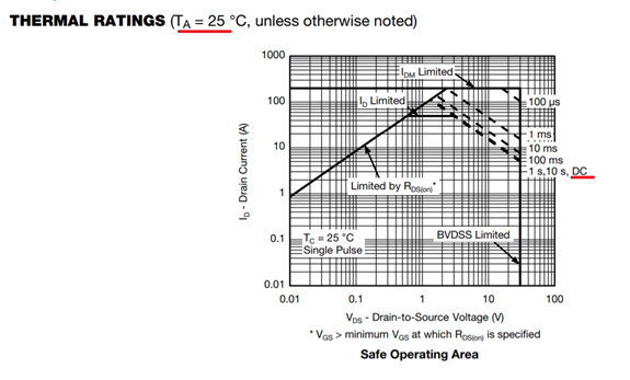
In addition, not all datasheets have a direct, limiting DC work area, although, for a rough estimate, this data can also be used.
The article will consider an example of calculating the maximum current through the MOSFET SQM50P03-07 (took the first one from its scheme), operating in the key mode, or in the saturation section.
First, a little theory to understand what is the essence of the problem. Who just needs to calculate the current - go straight to the practice.
Theory
In short, the main parameter that limits the maximum current through the PT is the temperature, or rather its growth. Even when operating in the key mode, when the current flows through the source-drain, the transistor has some resistance, for powerful MOSFET this value can be only a few mW (not the biggest and not the smallest value among PTs). When current passes through such a resistance, some power is dissipated on it (transforming into heat, the transistor heats up). The dissipated power is directly proportional to the square of the current passing through the PT.
')
The problem is that the maximum current (DC), like the maximum power dissipation, is often not indicated directly in the documentation, for example, the datasheet screen on SQM50P03-07:
Continuous Drain Current is 50 amps, but with a footnote that this is a limitation of the case, i.e. a current greater than this cannot physically pass through the body itself without destroying the structure.
Maximum Power Dissipation for different temperatures of 150 and 50 W, but with a footnote that this is when current is passed by pulses, where for 1 period 98% of the time the transistor is “turned off” and the remaining 2% is “on” (remember, we are interested in direct current) .
So, to calculate the maximum current through the PT, an important parameter here is the maximum temperature. From the datasheet it is clear that it is 175 ° C ( Operating Junction and Storage Temperature Range ), and it is necessary to make a start from it in calculations. It is necessary to determine which current will heat the semiconductor channel of the transistor to 175 ° C, but a further increase in temperature will not occur due to the transfer of heat to the environment (cooling), this will be the current value that we need.
Heating a transistor, like any other body, is a complex process and depends on many parameters. In order to maximally simplify the actions connected with thermal calculations, the thermal resistance parameter is introduced, i.e. the ability of something to prevent the spread of heat. The greater the thermal resistance, the slower the PT will cool, and the faster the temperature of its crystal will rise to a critical one. Also, the greater the difference between the maximum allowable temperature on the chip and the environment, the longer the PT will heat up, and the more current it will be possible to pass through it.
Each material has its own thermal resistance, and the transistor, in turn, consists of a substrate (body) on which a conductive channel is formed, an insulator, the body itself, which may also consist of several materials, of course they are also of different thickness, which affects heat transfer.
In addition, the transistor can also be cooled in different ways, on some, there is a large contact pad that is soldered to the board or attached to the radiator, in such cases the thermal resistance is minimal. Some transistors do not have such sites and are in contact with the environment only through a plastic case, through which heat is released much more slowly.
The result is approximately the following scheme:
Where
- T (Junction) is the temperature of the conducting channel inside the transistor (which heats up when current flows);
- T (Ambient) is the ambient temperature (where heat is removed);
- RT1-RT4 is the thermal resistance of materials that thermal energy overcomes.
With thermal resistance, as in electrical engineering, the rule works: “total resistance is equal to the sum of series resistances”.
As noted earlier, the PT can be cooled in different ways, and it is simply impossible to foresee all possible options in the datasheet, however, the most common ones are usually given:
- The PT is installed on the board without a radiator and without any heat-removing contact pads ( Junction-to-Ambient resistance);
- resistance is given to the substrate, Junction-to-Case (or to a certain point on the case from which heat is removed) , and then, depending on the application, for example, a radiator is attached to the substrate, then its resistance must be added to the system and the resistance of the gasket between it and the PT case (the heat sink can be very large and take on all the heat from the transistor, in this case the temperature of the environment will be considered the temperature of this radiator).
Thermal resistances are not always indicated directly on the page with the maximum PT parameters, for example, a screen from the Si4477DY documentation:
Although there is a Junction-to-Foot parameter, suppose we are interested in precisely the thermal resistance of Junction-to-Ambient , and it is given only for a time less than 10 seconds. In this case, you can rummage on the manufacturer's website and find models of thermal resistance. In such documents there is a graph of the dependence of the temperature difference Junction-Ambient on time:
The graph shows that after 1000 seconds, a significant increase in temperature change stops. In this mode, the temperature difference is numerically equal to the thermal resistance. Therefore, for direct current, you can focus on the value of 80 ° C / W - the thermal resistance of Junction-to-Ambient .
(a little more in the comments )
Maybe not all companies have this information, but all of them are mostly standard PT hulls, it is enough to find the resistance data for another hull of interest to us.
When the developer has determined how exactly the PT will cool, the ambient temperature in which the device will operate, after that, you can finally proceed to the calculation.
Practice
Consider an example of determining the maximum direct current through the MOSFET SQM50P03-07 in the key mode, which is soldered to a 300x300 mm board (without a radiator). The board will work in the air at a maximum temperature of 45 ° C. We will control the PT by applying a voltage of 5 volts to its gate.
1. TJMAX
MOSFET is heated in the area of the formed conductive channel (on the substrate under the insulator and gate), this is the temperature Tjunction (temperature at the junction). From the datasheet of the Operating Junction and Storage Temperature Range -55 ... +175 , since we are interested in the maximum current, then we take the maximum temperature, i.e. TJMAX = 175 ° C (if you don’t want the transistor channel to be so hot, you can take a lower value).
2. TA
Ambient temperature We take the maximum possible temperature to which the transistor will have to give off heat, according to the initial conditions TA = 45 ° C.
3. RΘJA
In the datasheet we find the thermal resistance of the conductive channel of the transistor to the environment, moreover, below there is a note that this resistance is relevant if the PT is soldered to a board larger than 1 inch square (in this case, some of the heat goes to the board, and with such dimensions, the necessary heat sink is carried out):
Thus, RΘJA = 40 ° C / W.
4. RDS (ON)
Maximum drain-source resistance at a certain control voltage at the gate. Information can be taken from the table, but the values of the channel resistance are given there only at gate voltages of 10V and 4.5V, while our plan is 5 volts. The difference, of course, is small, you can take 4.5V:
It’s better to find in the datasheet the dependence of the channel resistance on the voltage applied to the gate:
It is necessary to pay attention to the fact that in the case of the table, the data are given for TC = 25 ° C (substrate temperature), and in the case of the schedule there are 2 options: TJ = 25 ° C and TJ = 150 ° C (channel temperature). In the selected example, the channel will warm up to 175 ° C (as determined in the first calculation point). It turns out that at the moment it is better to use not the table, but the graph, to determine the channel resistance, since The value given in the table at TC = 25 ° C is not what we are interested in right now.
So, 8 mOhm (0.008 Ohm) is the resistance of the channel at its temperature of 25 ° C. To determine the resistance at a temperature TJMAX = 175 ° C, we look for a graph of the dependence of the normalized channel resistance on its temperature:
The horizontal axis is the connection temperature, and the vertical increment coefficient to the resistance. It can be noted that at 25 ° C it is equal to 1 (dimensionless value), i.e. the value that was previously determined (8 mΩ) is at this level. At a temperature of 175 ° C, the coefficient is about 1.69 .
To find the channel resistance at TJ = 175 ° C , multiply the resistance at 25 ° C by the coefficient at 175 ° C. We get 0.008 * 1.69 = 13.52 mΩ. RDS (ON) = 13.52 mΩ (0.013352 Ω) .
5. IDMAX
Now you can use the formula below to determine the maximum current (DC) that the transistor can skip:
We get 15,504 amps.
However, calculations using thermal models based on thermal resistances have an error that occurs due to the simplification of those same models. Therefore, it is recommended to make a current margin of at least 20% . We make the last calculation and get 12,403 amps . This is the current value that SQM50P03-07 can pass through itself in the saturation mode and not burn, at the initial conditions specified above.
Note how the value of 12 A differs from what is indicated on the first pages of the datasheet (50 A, 150 A), such figures are confusing at first, if you do not deal with all the nuances.
In conclusion, a few words about the Safe Operating Area , this is a diagram showing the areas of normal operation of the transistor in different modes. For the same SQM50P03-07 there is an SOA in the datasheet, however, as you can see, it is given for a channel temperature of 25 ° C (not our case)
In addition, not all datasheets have a direct, limiting DC work area, although, for a rough estimate, this data can also be used.
Source: https://habr.com/ru/post/446602/
All Articles