AMD announced its 3D chip architecture to catch up with Intel Foveros 3D
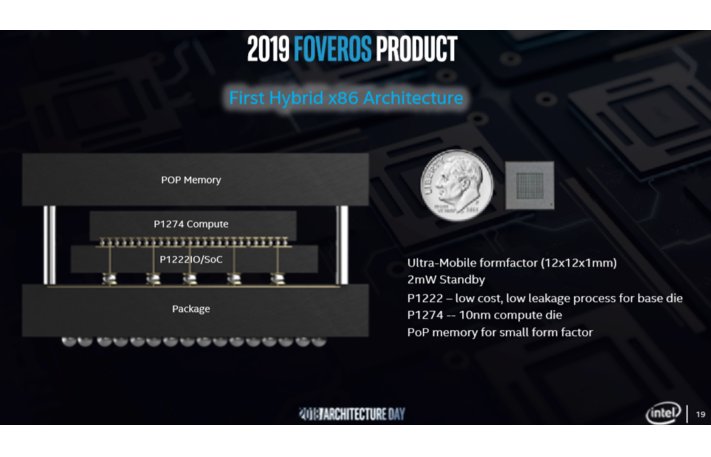
Intel Foveros 3D
Since Moore's law is no longer valid, chip designers have to look for other ways to improve performance. One suitable technology for this is called 3D chip stacking. This is the bulk shelf architecture of chips, in the development of which Intel leads. Two months ago, Intel introduced the Foveros 3D architecture: a three-dimensional structure that includes a CPU for a 10 nm process, an I / O chip, and TSV (Through Silicon Via) vertical electrical connections in the center of the chip, and a memory chip on top of the entire chip.
At a high-performance computing conference, Rice Oil and Gas HPC, AMD assured that it was working on its own version of the 3D chip architecture.
Senior Vice President and General Manager Forrest Norrod (Forrest Norrod) said that the company is developing several technologies to increase returns and circumvent problems due to the termination of Moore's law and the consequences - the termination of the increase in the density of transistors and clock frequency. These are the inevitable consequences of the fact that manufacturers are close to the limit, where the size of the transistor is only a few atoms (the size of the silicon atom is 0.2 nanometers). The growth of computer power in recent years comes not so much from an increase in the speed of calculations, but rather from an increase in parallelism.
')
Like other companies, AMD faced a restriction on the chip area of about 700 mm² and was forced to develop a 3D architecture. The company is already using this approach, placing the HBM2 memory next to the GPU substrate, that is, it is in the same package as the processor. But in the future, the company plans to move to more advanced 3D stacking.
Norrod said AMD is working on allocating SRAM and DRAM directly on top of computing components (for example, processors and graphics processors) to provide even greater bandwidth and performance.
Samsung polaris
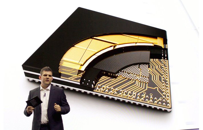
This approach differs from the usual package-on-package (PoP) implementations, which simply place two ready-made cases on top of each other, as Norrod showed with the example of the Samsung Polaris chip. In this example, the DRAM package is connected via two additional rows of BGA connectors that surround the base chip. These BGA connectors transfer data between two chips. As with any standard design, the logic is at the bottom of the stack due to the need for more connectors, but the two crystals are not directly connected. Thus, the PoP approach provides maximum density, but this is not the fastest option.
In true 3D stacking, the two chips (in this case, the memory and the processor) are located one above the other and are connected by vertical TSV connections that directly interface them. These TSV connections transfer data between the crystals as fast as possible and are usually located in the center of the chip, as we saw in the example of Intel Foveros 3D. This direct mate improves performance and reduces power consumption (all data movement requires power, but direct connections optimize the process). 3D stacking also increases density.
Norrod did not go deep into the details of the projects under development, but this may be a fundamental shift in the design of the AMD processor.
The new technology Intel Foveros 3D can be a defining moment for the industry, so it is not surprising to hear that AMD is moving in this direction, writes Tom's Hardware .
So far, there are no technical details about AMD's 3D stacking technology, except what Forrest Norrod said at the presentation entitled Working Beyond Moore's Law, see the video below.
What other alternatives are there to return to the exponential growth curve predicted by Gordon Moore? This question has no definite answer. The semiconductor industry is experimenting with materials that can be used instead of silicon. Some III-V semiconductor materials can operate at lower voltages and at higher frequencies than silicon , but they do not make the atoms smaller or the light slower. Physical limitations are still in force.
It remains an open question how future 3D chips will be cooled. How to effectively cool such a chip when energy is distributed everywhere inside it? The microcircuit will not be able to transmit power to all circuits at the same time without overheating. Probably, she will have to keep some parts off for most of the time and supply power to each part only during its use.
Source: https://habr.com/ru/post/444252/
All Articles