Making ST-Link V2.1 from Chinese ST-Link V2
 Hi, Habr!
In this article I will explain how to modify ST-Link V2 to ST-Link V2.1.
Perhaps for someone it will not be news, but I did not find much information on this topic in the internet.
')
Who cares - I ask under the cat.
Foreword
It so happened that I was bored with extra wires.
A little thought, I remembered that on the boards Nucleo and Discovery - ST-Link combines SWD and VCP (Virtual Com Port).
The first thing that occurred to me was to buy the cheapest of such cards, try to dump the firmware around the protection and upload it to the programmer from China, or dissolve the new board.
However, I was prompted to link to GitHub with an already extended bootloader, which eventually resulted in what happened.
Getting Started
Modification can be made only on the version of the software under Windows, the cross-platform version of the software refuses to update the device!
There are several options for modification, and some of them can not be done if the chip is not suitable (not enough memory).
For example, a modification of STM32 + MSD + VCP can be done only if the chip is STM32F1xxCBxx, but it has an analogue of STM32 + Audio, which will give STM32 + VCP (in principle, what we need).
It will take:
- Soldering iron;
- Multimeter with dialing;
- PC with Windows OS (maybe it will work through Wine, I haven't tried it);
- Archive with the necessary software and bootloader (PASS: QWK2tn + fM.EdjX6z).
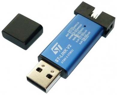
- Chinese clone ST-Link V2;
- USB-UART adapter or second ST-Link.
We open ...
Boards and chips in all different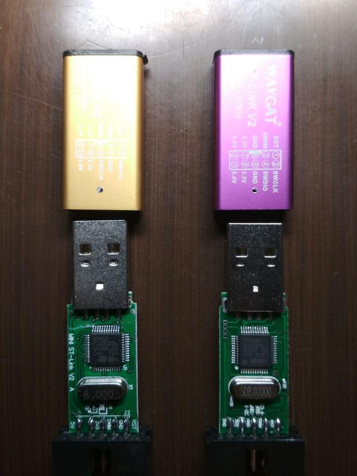
Firmware
There are two ways - USB-UART (slightly more complicated) or the second ST-Link.
USB UART
1) With a dial, we find a resistor that is connected to BOOT0 .
Make a jumper from the side of this resistor which is connected to BOOT0 to 3.3v .
PA9 (TX) can be connected to the LED or resistor next to it, so we call it.
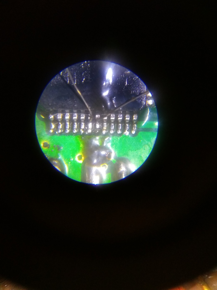
We solder the UART on PA9 ( TX ) and PA10 ( RX ).
I did it like this:
Just solder the food.
We are flashing the Protected-2-1-Bootloader.bin loader using the STM32 Flash loader demonstrator .
After flashing, unplug the jumper, PA9 and PA10 (leave the PA10 if we want to output SWO ).
1) With a dial, we find a resistor that is connected to BOOT0 .
Make a jumper from the side of this resistor which is connected to BOOT0 to 3.3v .
PA9 (TX) can be connected to the LED or resistor next to it, so we call it.
We solder the UART on PA9 ( TX ) and PA10 ( RX ).
I did it like this:
Just solder the food.
We are flashing the Protected-2-1-Bootloader.bin loader using the STM32 Flash loader demonstrator .
After flashing, unplug the jumper, PA9 and PA10 (leave the PA10 if we want to output SWO ).
ST-Link
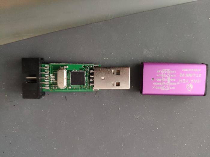
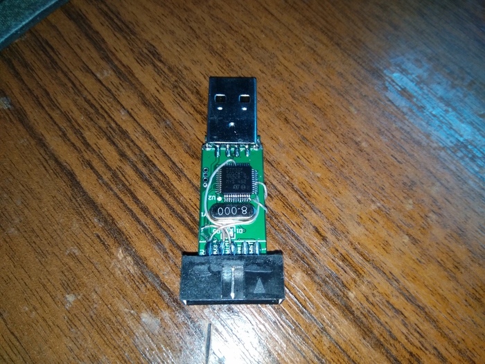
On the boards there are 4 pins each , in some cases they are already marked, otherwise we call them relative to PA13 ( SWDIO ) and PA14 ( SWCLK ), we solder with the second ST-Link .

Just solder the food.
Install the STM32 ST-LINK Utility V4.3 from the archive, remove the write protection and flash the loader Protected-2-1-Bootloader.bin.
To remove protection in the STM32 ST-LINK Utility program, click Target> Option Bytes , switch Read Out Protection to Disabled, and click Apply .
On the boards there are 4 pins each , in some cases they are already marked, otherwise we call them relative to PA13 ( SWDIO ) and PA14 ( SWCLK ), we solder with the second ST-Link .
Just solder the food.
Install the STM32 ST-LINK Utility V4.3 from the archive, remove the write protection and flash the loader Protected-2-1-Bootloader.bin.
To remove protection in the STM32 ST-LINK Utility program, click Target> Option Bytes , switch Read Out Protection to Disabled, and click Apply .
Upgrade to ST-Link V2.1
After the firmware, connect the stitched ST-Link (now almost V2.1) to the PC.
In the STM32 ST-LINK Utility V4.3 program, click ST-LINK> Firmware update .
Click Device Connect - we get a list of possible modifications:

Select the modification you need, in my case STM32 + MSD + VCP , click Yes >>>> .
We are waiting for the update to complete ...
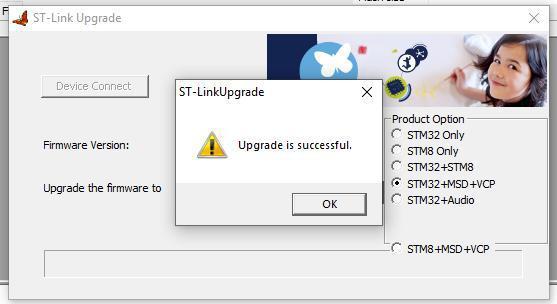
Profit!
The final part
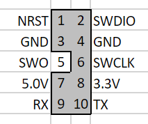
Since SWIM and RST do not work after this modification, I cut them off.
I also cut off the backup 5V and 3.3V.
It turns out 4 free pins.
On them I get wired to the chip:
PA10 -> SWO
PB0 -> NRST
PA3 -> RX
PA2 -> TX
I bring everything to the main connector, to the remaining free pins.
It turned out this pinout:
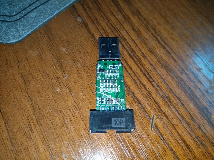
My device after modification
Nakaryabal scalpel markings on the body:

Nakaryabal scalpel markings on the body:
Do not forget to wash the board after soldering!
As a result, in the PC device is determined as follows:
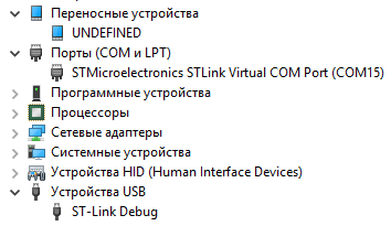
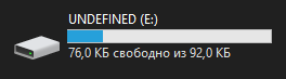
I have no idea what is equal to the amount of virtual flash drives (in this case, F103C8 was connected to ST-Link V2.1).
If you drop the firmware file onto it, the programmer will flash the chip without programs.
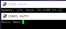
Checking VCP:
Thanks for attention!
With questions, please contact the comments, if I can - I will help.
Source: https://habr.com/ru/post/442290/
All Articles