Perspective: MultiClet S1
So, it's time to talk about the next generation of multicellular processors: MultiClet S1. If you hear about them for the first time, be sure to check out the history and ideology of architecture in these articles:
- “Multicellular processor is what?”
- "Multiclet R1 - the first tests"
- “LLVM-based C / C ++ compiler for multicellular processors: to be or not to be?”
At the moment, the new processor is in development, but the first results have already appeared and you can evaluate what it will be capable of.
Let's start with the biggest changes: basic characteristics.
')
Specifications.
It is planned to achieve the following indicators:
- Cell Number: 64
- Process technology: 28 nm
- Clock frequency: 1.6 GHz
- Memory size on a crystal: 8 MB
- Crystal area: 40mm 2
- Power Consumption: 6 W
Real numbers will be announced on the results of tests of fabricated samples in 2019. In addition to the characteristics of the chip, the processor will support up to 16 GB of DDR4 3200MHz standard RAM, PCI Express bus and PLL.
It should be noted that the technical process of 28 nm is the lowest household range that does not require special permissions to use, so he was chosen. According to the number of cells, different options were considered: 128 and 256, but with an increase in the area of the crystal, the reject rate increases. We stopped at 64 cells and, accordingly, a relatively small area, which would give a greater yield of suitable crystals on the plate. Further development is possible within the framework of the SVK (system in the case) , where it will be possible to combine several 64-cell crystals into one case.
It must be said that the purpose and application of the processor is changing dramatically. S1 is not a microprocessor designed for embedding, as P1 and R1 were, but a computation accelerator. Just like GPGPU, a board with S1 can be inserted into the PCI Express motherboard of a regular PC and used for data processing.
Architecture
In S1, the minimal computational unit is now the “multicell”: a set of 4 cells that execute a certain sequence of commands. At first, it was planned to merge multi-cells into groups called cluster for joint execution of commands: the cluster had to contain 4 multi-cells, all on a crystal, 4 separate clusters. However, each cell has a full connection with all the other cells in the cluster, and as the group of links increases, it becomes too much, which greatly complicates the topological design of the chip and reduces its characteristics. Therefore, it was decided to abandon cluster division, since the complication does not justify the results obtained. In addition, for maximum performance, it is most advantageous to run the code in parallel on each multicell. Total, now the processor contains 16 separate multi-cells.
The multicell, although it consists of 4 cells, differs from 4-cell R1, in which each cell had its own memory, its own unit of selection of commands, its own ALU. S1 is a bit different. ALU has 2 parts: a floating point arithmetic unit and an integer arithmetic unit. Each cell has a separate integer block, but there are only two floating-point blocks in the multicell, and therefore two pairs of cells divide them among themselves. This was done mainly to reduce the crystal area: 64-bit floating point arithmetic, unlike integer arithmetic, takes up a lot of space. Having such an ALU block on each cell turned out to be redundant: the selection of commands does not ensure the loading of ALUs and they are idle. When reducing the number of ALUs and maintaining the rate of sampling of commands and data, as practice has shown, the total time for solving problems practically does not change or changes slightly, and ALUs are loaded completely. In addition, floating point arithmetic is not used as often as with integer.
A schematic view of the blocks of processors R1 and S1 is shown in the diagram below. Here:
- CU (Control Unit) - block selection instructions
- ALU FX - arithmetic logic unit of integer arithmetic
- ALU FP - an arithmetic-logical device for floating-point arithmetic
- DMS (Data Memory Scheduler) - data memory management unit
- DM - data memory
- PMS (Program Memory Scheduler) - program memory management unit
- PM - program memory

Architectural differences S1:
- Teams can now access the results of teams from the previous paragraphs. This is a very important change that allows you to significantly speed up transitions during code branching. In the P1 and R1 processors there was no other choice than to write the necessary results into memory and immediately read them back with the first commands in the new paragraph. Even when using memory on a chip, the write and read operations take 2 to 5 cycles each, which can be saved by simply referring to the result of the command from the previous paragraph.
- Memory and registers are now written immediately, and not at the end of a paragraph, which allows you to start executing write commands before the end of a paragraph. As a result, the potential downtime between paragraphs is reduced.
- Optimized command system, namely:
- Added 64-bit integer arithmetic: addition, subtraction, multiplication of 32-bit numbers, which returns a 64-bit result.
- Changed the way of reading from memory: now for any command as an argument, you can simply specify the address from which you want to read the data, while maintaining the order of execution of commands read and write.
It also made a separate memory read command obsolete. Instead, use the command to load the value into the load switch (previously - get ), specifying an address in memory as an argument:.data foo: .long 0x1234 .text habr: load_l foo ; foo load_l [foo] ; 0x1234 add_l [foo], 0xABCD ; ; complete - Command format has been added, allowing to use 2 constant arguments.
Previously, it was possible to specify a constant only as a second argument, the first argument should always be a reference to the result in the switch. The change concerns all two-team teams. The constant field is always 32 bit, so this format allows, for example, to generate 64-bit constants with one command.
It was:load_l 0x12345678 patch_q @1, 0xDEADBEEF
It became:patch_q 0x12345678, 0xDEADBEEF - Changed and added vector data types.
What was previously called “packed” data types can now be safely called vector ones. In P1 and R1, operations on packed numbers took only a constant as the second argument, that is, for example, when adding, each element of the vector was added to the same number, and there was no sensible use for this. Now similar operations can be applied over two full-fledged vectors. Moreover, this way of working with vectors is fully consistent with the mechanism of vectors in LLVM, which now allows the compiler to generate code using vector types.patch_q 0x00010002, 0x00030004 patch_q 0x00020003, 0x00040005 mul_ps @1, @2 ; - 00020006000C0014
- Removed processor flags.
As a result, about 40 teams have been removed, based solely on the values of the flags. This has significantly reduced the number of teams and, accordingly, the crystal area. And all the necessary information is now stored directly in the switch cell.- When comparing with zero, instead of the zero flag, now just the value in the switch is used
- Instead of the sign flag, the bit corresponding to the type of command is now used: 7th for byte, 15th for short, 31st for long, 63th for quad. Due to the fact that the sign multiplies up to the 63rd bit, regardless of the type, you can compare the numbers of different types:
.data long: .long -0x1000 byte: .byte -0x10 .text habr: a := load_b [byte] ; 0xFFFFFFFFFFFFFFF0, ; byte 7 63. b := loadu_b [byte] ; 0x00000000000000F0, ; .. loadu_b c := load_l [long] ; 0xFFFFFFFFFFFFF000. ge_l @a, @c ; " " 1: ; 31 , . lt_s @a, @b ; 1, .. b complete - The carry flag is no longer needed, since there is 64-bit arithmetic
- The transition time from a paragraph to a paragraph has decreased to 1 cycle (instead of 2-3 in R1)
LLVM Compiler
The C compiler for S1 is similar to R1, and since the architecture has not fundamentally changed, the problems described in the previous article, unfortunately, have not disappeared.
However, in the process of implementing the new command system, the amount of the output code decreased by itself, simply due to the update of the command system. In addition, there are many other small optimizations that will reduce the number of commands in the code, some of which have already been made (for example, generating 64-bit constants with one command). But there are even more serious optimizations that need to be done, and they can be built in ascending order at the same time as the efficiency and complexity of implementation:
- The ability to generate all two-team commands with two constants.
Generating a 64-bit constant through patch_q is just a special case, but a common one is needed. In fact, the point of this optimization is to allow teams to substitute the first argument as a constant, since the second argument could always be a constant, and this has long been implemented. This is not a very frequent case, but, for example, when you need to call a function and write the return address from it to the top of the stack, you canload_l func wr_l @1, #SP
optimize upwr_l func, #SP - The ability to substitute memory access through an argument in any command.
For example, if you want to add two numbers from the memory, you canload_l [foo] load_l [bar] add_l @1, @2
optimize upadd_l [foo], [bar]
This optimization is an extension of the previous one, however, an analysis is already needed here: such a replacement can be carried out only if the loaded values are used only once in this addition command and nowhere else. If the reading result is used even in only two commands, then it is more advantageous to read from memory once as a separate command, and in the other two to refer to it through the switch. - Optimizing the transfer of virtual registers between base blocks.
For R1, the transfer of all virtual registers was done through memory, which causes a very large number of reads and entries in memory, but there was simply no other way to transfer data between paragraphs. S1 allows you to refer to the results of the commands of previous sections, therefore, theoretically, many memory operations can be removed, which would give the greatest effect among all optimizations. However, this approach is still limited to the switch: no more than 63 previous results, so not every transfer of the virtual register can be implemented like this. How to do this is a non-trivial task, and an analysis of its solution possibilities is still to be done. The source code of the compiler may appear in the public domain, so if someone has ideas and you want to join the development, then you can do it.
Benchmarks
Since the processor has not yet been released on a chip, it is difficult to assess its actual performance. However, the RTL core code is already ready, which means you can make an estimate using simulation or FPGA. To run the following benchmarks, we used simulation using the ModelSim program to calculate the exact execution time (in ticks). Since it is difficult to simulate the whole crystal, it takes a lot of time, so a single multicell was modeled, and the result was multiplied by 16 (if the task is designed for multithreading), since each multicell can work completely independently of the others.
Simultaneously, the simulation of a multicell on Xilinx Virtex-6 was carried out to check the performance of the processor code on real hardware.
Coremark
CoreMark - a set of tests for a comprehensive assessment of the performance of microcontrollers and CPUs, as well as their C-compilers. As you can see, the S1 processor is neither. However, it is designed to execute an absolutely arbitrary code, i.e. anyone that could be running on a central processor. This means CoreMark is suitable for evaluating the performance of S1 just as good.
CoreMark contains work with linked lists, matrices, state machine and CRC sum calculation. In general, most of the code is strictly sequential (which tests multi-cell hardware parallelism for durability) and with many branches, which makes the compiler's capabilities play a significant role in the final performance. The compiled code contains quite a few short paragraphs, and despite the fact that the transition rate between them has increased, branching involves working with memory, which we would like to avoid to the maximum.
Comparative table of CoreMark indicators:
| Multiclet R1 (llvm compiler) | Multiclet S1 (llvm compiler) | Elbrus-4C (R500 / E) | Texas Inst. AM5728 ARM Cortex-A15 | Baikal-T1 | Intel Core i7 7700K | |
|---|---|---|---|---|---|---|
| Year of issue | 2015 | 2019 | 2014 | 2018 | 2016 | 2017 |
| Clock frequency, MHz | 100 | 1600 | 700 | 1500 | 1200 | 4500 |
| CoreMark Total | 59 | 18356 | 1214 | 15789 | 13142 | 182128 |
| CoreMark / MHz | 0.59 | 11.47 | 5.05 | 10.53 | 10.95 | 40.47 |
The result of a single multicell is 1147, or 0.72 / MHz, which is higher than that of R1. This shows the advantages of developing a multi-cellular architecture in the new processor.
Whetstone
Whetstone is a set of tests for measuring CPU performance when working with floating point numbers. Here the situation is much better: the code is also sequential, but without a large number of branches and with good internal parallelism.
Whetstone consists of a set of modules that allows you to measure not only the overall result, but also the performance on each specific module:
- Array elements
- Array as parameter
- Conditional jumps
- Integer arithmetic
- Trigonometric functions (tan, sin, cos)
- Procedure calls
- Array references
- Standard functions (sqrt, exp, log)
They are broken down into categories: modules 1, 2, and 6 measure the performance of floating point operations (strings MFLOPS1-3); modules 5 and 8 - mathematical functions (COS MOPS, EXP MOPS); modules 4 and 7 - integer arithmetic (FIXPT MOPS, EQUAL MOPS); Module 3 - conditional transitions (IF MOPS). In the table below, the second line of MWIPS is the overall figure.
Unlike CoreMark, Whetstone will be compared on a single core or, as in our case, on a single multicell. Since the number of cores is very different in different processors, then, for the purity of the experiment, we consider the indicators calculated per megahertz.
Whetstone comparison chart:
| CPU | MultiClet R1 | MultiClet S1 | Core i7 4820K | ARM v8-A53 |
|---|---|---|---|---|
| Frequency, MHz | 100 | 1600 | 3900 | 1300 |
| MWIPS / MHz | 0.311 | 0.343 | 0.887 | 0.642 |
| MFLOPS1 / MHz | 0.157 | 0.156 | 0.341 | 0.268 |
| MFLOPS2 / MHz | 0.153 | 0.111 | 0.308 | 0.241 |
| MFLOPS3 / MHz | 0.029 | 0.124 | 0.167 | 0.239 |
| COS MOPS / MHz | 0.018 | 0.008 | 0.023 | 0.028 |
| EXP MOPS / MHz | 0.008 | 0.005 | 0.014 | 0.004 |
| FIXPT MOPS / MHz | 0.714 | 0.116 | 0.998 | 1.197 |
| IF MOPS / MHz | 0.081 | 0.196 | 1.504 | 1.436 |
| EQUAL MOPS / MHz | 0.143 | 0.149 | 0.251 | 0.439 |
Whetstone contains much more direct computing operations than CoreMark (which is very noticeable when looking at the code below), so it’s important to remember: the number of floating-point ALUs is halved. However, the speed of the calculations almost did not suffer, compared to R1.
Some modules fit the multicellular architecture very well. For example, module 2 considers a set of values in a cycle, and thanks to the full support of double-precision floating-point numbers as a processor and a compiler, after compilation, large and beautiful paragraphs are obtained, where the computational capabilities of the multicellular architecture are really revealed:
Big and beautiful paragraph on 120 teams
pa: SR4 := loadu_q [#SP + 16] SR5 := loadu_q [#SP + 8] SR6 := loadu_l [#SP + 4] SR7 := loadu_l [#SP] setjf_l @0, @SR7 SR8 := add_l @SR6, 0x8 SR9 := add_l @SR6, 0x10 SR10 := add_l @SR6, 0x18 SR11 := loadu_q [@SR6] SR12 := loadu_q [@SR8] SR13 := loadu_q [@SR9] SR14 := loadu_q [@SR10] SR15 := add_d @SR11, @SR12 SR11 := add_d @SR15, @SR13 SR15 := sub_d @SR11, @SR14 SR11 := mul_d @SR15, @SR5 SR15 := add_d @SR12, @SR11 SR12 := sub_d @SR15, @SR13 SR15 := add_d @SR14, @SR12 SR12 := mul_d @SR15, @SR5 SR15 := sub_d @SR11, @SR12 SR16 := sub_d @SR12, @SR11 SR17 := add_d @SR11, @SR12 SR11 := add_d @SR13, @SR15 SR13 := add_d @SR14, @SR11 SR11 := mul_d @SR13, @SR5 SR13 := add_d @SR16, @SR11 SR15 := add_d @SR17, @SR11 SR16 := add_d @SR14, @SR13 SR13 := div_d @SR16, @SR4 SR14 := sub_d @SR15, @SR13 SR15 := mul_d @SR14, @SR5 SR14 := add_d @SR12, @SR15 SR12 := sub_d @SR14, @SR11 SR14 := add_d @SR13, @SR12 SR12 := mul_d @SR14, @SR5 SR14 := sub_d @SR15, @SR12 SR16 := sub_d @SR12, @SR15 SR17 := add_d @SR15, @SR12 SR15 := add_d @SR11, @SR14 SR11 := add_d @SR13, @SR15 SR14 := mul_d @SR11, @SR5 SR11 := add_d @SR16, @SR14 SR15 := add_d @SR17, @SR14 SR16 := add_d @SR13, @SR11 SR11 := div_d @SR16, @SR4 SR13 := sub_d @SR15, @SR11 SR15 := mul_d @SR13, @SR5 SR13 := add_d @SR12, @SR15 SR12 := sub_d @SR13, @SR14 SR13 := add_d @SR11, @SR12 SR12 := mul_d @SR13, @SR5 SR13 := sub_d @SR15, @SR12 SR16 := sub_d @SR12, @SR15 SR17 := add_d @SR15, @SR12 SR15 := add_d @SR14, @SR13 SR13 := add_d @SR11, @SR15 SR14 := mul_d @SR13, @SR5 SR13 := add_d @SR16, @SR14 SR15 := add_d @SR17, @SR14 SR16 := add_d @SR11, @SR13 SR11 := div_d @SR16, @SR4 SR13 := sub_d @SR15, @SR11 SR4 := loadu_q @SR4 SR5 := loadu_q @SR5 SR6 := loadu_q @SR6 SR7 := loadu_q @SR7 SR15 := mul_d @SR13, @SR5 SR8 := loadu_q @SR8 SR9 := loadu_q @SR9 SR10 := loadu_q @SR10 SR13 := add_d @SR12, @SR15 SR12 := sub_d @SR13, @SR14 SR13 := add_d @SR11, @SR12 SR12 := mul_d @SR13, @SR5 SR13 := sub_d @SR15, @SR12 SR16 := sub_d @SR12, @SR15 SR17 := add_d @SR15, @SR12 SR15 := add_d @SR14, @SR13 SR13 := add_d @SR11, @SR15 SR14 := mul_d @SR13, @SR5 SR13 := add_d @SR16, @SR14 SR15 := add_d @SR17, @SR14 SR16 := add_d @SR11, @SR13 SR11 := div_d @SR16, @SR4 SR13 := sub_d @SR15, @SR11 SR15 := mul_d @SR13, @SR5 SR13 := add_d @SR12, @SR15 SR12 := sub_d @SR13, @SR14 SR13 := add_d @SR11, @SR12 SR12 := mul_d @SR13, @SR5 SR13 := sub_d @SR15, @SR12 SR16 := sub_d @SR12, @SR15 SR17 := add_d @SR15, @SR12 SR15 := add_d @SR14, @SR13 SR13 := add_d @SR11, @SR15 SR14 := mul_d @SR13, @SR5 SR13 := add_d @SR16, @SR14 SR15 := add_d @SR17, @SR14 SR16 := add_d @SR11, @SR13 SR11 := div_d @SR16, @SR4 SR13 := sub_d @SR15, @SR11 SR15 := mul_d @SR13, @SR5 SR13 := add_d @SR12, @SR15 SR12 := sub_d @SR13, @SR14 SR13 := add_d @SR11, @SR12 SR12 := mul_d @SR13, @SR5 SR13 := sub_d @SR15, @SR12 SR16 := sub_d @SR12, @SR15 SR17 := add_d @SR14, @SR13 SR13 := add_d @SR11, @SR17 SR14 := mul_d @SR13, @SR5 SR5 := add_d @SR16, @SR14 SR13 := add_d @SR11, @SR5 SR5 := div_d @SR13, @SR4 wr_q @SR15, @SR6 wr_q @SR12, @SR8 wr_q @SR14, @SR9 wr_q @SR5, @SR10 complete popcnt
To reflect the characteristics of the architecture itself (without dependence on the compiler), measure something written in assembly language with all the features of the architecture. For example, counting single bits in a 512-bit number (popcnt). For obviousness, we will take the results of a single multicell so that they can be compared with R1.
Comparison table, the number of cycles per calculation cycle 32 bits:
| Algorithm | Multiclet R1 | Multiclet S1 (one multicell) |
|---|---|---|
| Bithacks | 5.0 | 2.625 |
Here new updated vector instructions were used, which made it possible to reduce the number of instructions by half compared to the same algorithm implemented in R1 assembler. The speed of work, respectively, increased by almost 2 times.
popcnt
bithacks: b0 := patch_q 0x1, 0x1 v0 := loadu_q [v] v1 := loadu_q [v+8] v2 := loadu_q [v+16] v3 := loadu_q [v+24] v4 := loadu_q [v+32] v5 := loadu_q [v+40] v6 := loadu_q [v+48] v7 := loadu_q [v+56] b1 := patch_q 0x55555555, 0x55555555 i00 := slr_pl @v0, @b0 i01 := slr_pl @v1, @b0 i02 := slr_pl @v2, @b0 i03 := slr_pl @v3, @b0 i04 := slr_pl @v4, @b0 i05 := slr_pl @v5, @b0 i06 := slr_pl @v6, @b0 i07 := slr_pl @v7, @b0 b2 := patch_q 0x33333333, 0x33333333 i10 := and_q @i00, @b1 i11 := and_q @i01, @b1 i12 := and_q @i02, @b1 i13 := and_q @i03, @b1 i14 := and_q @i04, @b1 i15 := and_q @i05, @b1 i16 := and_q @i06, @b1 i17 := and_q @i07, @b1 b3 := patch_q 0x2, 0x2 i20 := sub_pl @v0, @i10 i21 := sub_pl @v1, @i11 i22 := sub_pl @v2, @i12 i23 := sub_pl @v3, @i13 i24 := sub_pl @v4, @i14 i25 := sub_pl @v5, @i15 i26 := sub_pl @v6, @i16 i27 := sub_pl @v7, @i17 i30 := and_q @i20, @b2 i31 := and_q @i21, @b2 i32 := and_q @i22, @b2 i33 := and_q @i23, @b2 i34 := and_q @i24, @b2 i35 := and_q @i25, @b2 i36 := and_q @i26, @b2 i37 := and_q @i27, @b2 i40 := slr_pl @i20, @b3 i41 := slr_pl @i21, @b3 i42 := slr_pl @i22, @b3 i43 := slr_pl @i23, @b3 i44 := slr_pl @i24, @b3 i45 := slr_pl @i25, @b3 i46 := slr_pl @i26, @b3 i47 := slr_pl @i27, @b3 b4 := patch_q 0x4, 0x4 i50 := and_q @i40, @b2 i51 := and_q @i41, @b2 i52 := and_q @i42, @b2 i53 := and_q @i43, @b2 i54 := and_q @i44, @b2 i55 := and_q @i45, @b2 i56 := and_q @i46, @b2 i57 := and_q @i47, @b2 i60 := add_pl @i50, @i30 i61 := add_pl @i51, @i31 i62 := add_pl @i52, @i32 i63 := add_pl @i53, @i33 i64 := add_pl @i54, @i34 i65 := add_pl @i55, @i35 i66 := add_pl @i56, @i36 i67 := add_pl @i57, @i37 b5 := patch_q 0xf0f0f0f, 0xf0f0f0f i70 := slr_pl @i60, @b4 i71 := slr_pl @i61, @b4 i72 := slr_pl @i62, @b4 i73 := slr_pl @i63, @b4 i74 := slr_pl @i64, @b4 i75 := slr_pl @i65, @b4 i76 := slr_pl @i66, @b4 i77 := slr_pl @i67, @b4 b6 := patch_q 0x1010101, 0x1010101 i80 := add_pl @i70, @i60 i81 := add_pl @i71, @i61 i82 := add_pl @i72, @i62 i83 := add_pl @i73, @i63 i84 := add_pl @i74, @i64 i85 := add_pl @i75, @i65 i86 := add_pl @i76, @i66 i87 := add_pl @i77, @i67 b7 := patch_q 0x18, 0x18 i90 := and_q @i80, @b5 i91 := and_q @i81, @b5 i92 := and_q @i82, @b5 i93 := and_q @i83, @b5 i94 := and_q @i84, @b5 i95 := and_q @i85, @b5 i96 := and_q @i86, @b5 i97 := and_q @i87, @b5 iA0 := mul_pl @i90, @b6 iA1 := mul_pl @i91, @b6 iA2 := mul_pl @i92, @b6 iA3 := mul_pl @i93, @b6 iA4 := mul_pl @i94, @b6 iA5 := mul_pl @i95, @b6 iA6 := mul_pl @i96, @b6 iA7 := mul_pl @i97, @b6 iB0 := slr_pl @iA0, @b7 iB1 := slr_pl @iA1, @b7 iB2 := slr_pl @iA2, @b7 iB3 := slr_pl @iA3, @b7 iB4 := slr_pl @iA4, @b7 iB5 := slr_pl @iA5, @b7 iB6 := slr_pl @iA6, @b7 iB7 := slr_pl @iA7, @b7 wr_q @iB0, c wr_q @iB1, c+8 wr_q @iB2, c+16 wr_q @iB3, c+24 wr_q @iB4, c+32 wr_q @iB5, c+40 wr_q @iB6, c+48 wr_q @iB7, c+56 complete Ethereum
Benchmarks are, of course, good, but we have a specific task: to make a computing accelerator, and it would be nice to know how he handles real tasks. Modern cryptocurrencies are the best suited for such a check, because mining algorithms run on many different devices and therefore can serve as a benchmark for comparison. We started with Ethereum and the Ethash algorithm, which runs directly on the mining device.
The choice of Ethereum was due to the following considerations. As you know, algorithms such as Bitcoin are very effectively implemented by specialized ASIC chips, so the use of processors or video cards for mining Bitcoin and its clones becomes uneconomical due to low productivity and high power consumption. The community of miners, in an attempt to escape from this situation, develops cryptocurrency on other algorithmic principles, focusing on the development of algorithms that are used for mining general-purpose processors or video cards. This trend is likely to continue in the future. Ethereum is the most famous cryptocurrency based on this approach. The main mining tool for Ethereum is video cards, which are significantly (several times) more efficient than general-purpose processors (hashrate / TDP).
Ethash is the so-called memory bound algorithm, i.e. the time of its calculation is limited primarily by the amount and speed of memory, and not the speed of the calculations themselves. Now for mining Ethereum video cards are the best suited, but their ability to simultaneously perform many operations does not help much, and they still run up against the speed of the RAM, which is clearly demonstrated in this article . From there you can also take a picture illustrating the operation of the algorithm to explain why this happens.
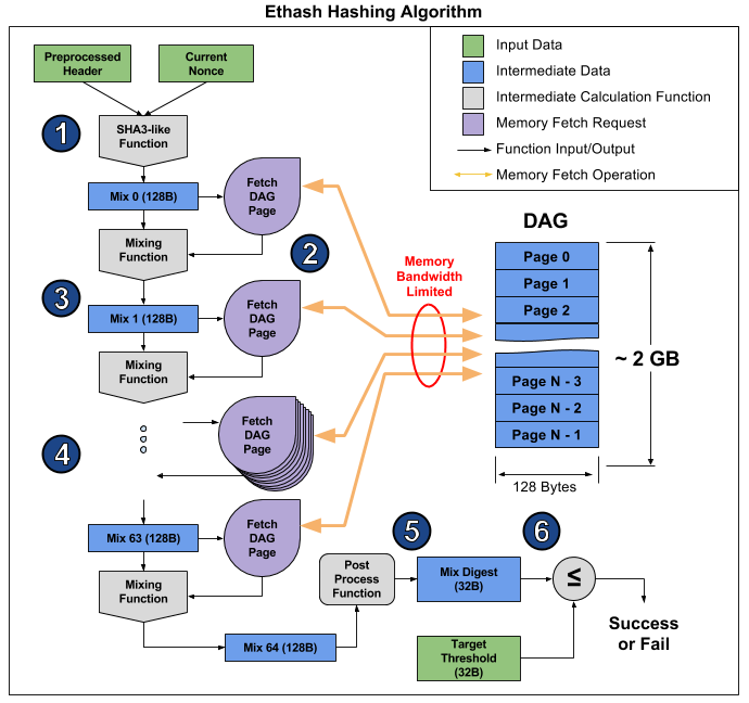
The article breaks the algorithm into 6 points, but you can select 3 steps for even more obviousness:
- Start: SHA-3 (512) to calculate the initial 128-byte mix 0 (item 1)
- 64-fold recalculation of the Mix array by reading the next 128 bytes and mixing them with the previous ones through the mixing function, a total of 8 kilobytes (steps 2-4)
- Finalizing and checking the result
Reading random 128 bytes from RAM takes much longer than it seems. If you take the MSI RX 470 video card, which has 2048 computing devices and a maximum memory bandwidth of 211.2 GB / s, then in order to provide each device you will need 1 / (211.2 GB / (128 b * 2048)) = 1241 ns, or approximately 1496 cycles at a given frequency. Considering the size of the mixing function, it can be assumed that the video card takes several times longer to read the memory than to recalculate the information received. As a result, stage 2 of the algorithm takes a very long time, much longer than stages 1 and 3, which ultimately have little effect on performance, despite the fact that they contain more calculations (mainly in SHA-3). You can just look at the hash rate of this video card: 26.375 megaheshesh / s theoretical (limited only by memory bandwidth) versus 24 megahesheshs / s actual, that is, stages 1 and 3 take only 10% of the time.
On S1, all 16 multi-cells can work in parallel and on different code. In addition, dual-channel RAM will be installed, one channel per 8 multicell cells. At stage 2 of the Ethash algorithm, our plan is as follows: one multicell reads 128 bytes from memory and starts their recalculation, then the next reads memory and performs recalculation and so on to the 8th, i.e. one multicell, after reading 128 bytes of memory, has 7 * [read time 128 bytes] on the recalculation of the array. It is assumed that such a reading will take 16 cycles, i.e. 112 cycles are given for recalculation. The calculation of the mixing function takes us about the same clock cycles, so S1 is close to the ideal ratio of memory bandwidth to the performance of the processor itself. Since time is not wasted on the second stage, the remaining parts of the algorithm should be optimized as much as possible, because then they really affect performance.
To estimate the speed of calculation of SHA-3 (Keccak), a program in C was developed and tested, on the basis of which its optimal version is currently being assembled. Estimated programming shows that one multicell performs SHA-3 (Keccak) calculation in 1550 cycles. Consequently, the total time to calculate one hash by one multicell will be 1550 + 64 * (16 + 112) = 9742 cycles. With a frequency of 1.6 GHz and 16 parallel multi-cells, the processor's hashrate will be 2.6 MHash / s.
| Accelerator | MultiClet S1 | NVIDIA GeForce GTX 980 Ti | Radeon RX 470 | Radeon RX Vega 64 | NVIDIA GeForce GTX 1060 | NVIDIA GeForce GTX 1080 Ti |
|---|---|---|---|---|---|---|
| Price | $ 650 | $ 180 | $ 500 | $ 300 | $ 700 | |
| Hashrate | 2.6 MHash / s | 21.6 MHash / s | 25.8 MHash / s | 43.5 MHash / s | 25 MHash / s | 55 MHash / s |
| Tdp | 6 W | 250 W | 120 W | 295 W | 120 W | 250 W |
| Hashrate / tdp | 0.43 | 0.09 | 0.22 | 0.15 | 0.22 | 0.21 |
| Technical process | 28 nm | 28 nm | 14 nm | 14 nm | 16 nm | 16 nm |
When using MultiClet S1 as a tool for mining, on the board can actually be installed 20 or more processors. In this case, the hash rate of such a card will be equal to or exceed the hashrates of existing video cards, while the power consumption of the card with S1 will be two times less than that of video cards with toonorms of 16 and 14 nm.
In conclusion, I must say that the main task now is to manufacture a multiprocessor board for the multicellular miner of cryptocurrency and supercomputing. Competitiveness is planned to achieve at the expense of low power consumption and architecture, well suited for arbitrary calculations.
The processor is still in development, but you can already start programming in assembly language, as well as evaluate the current version of the compiler. There is already a minimum SDK containing an assembler, a linker, a compiler, and a functional model on which you can run and test your programs.
Source: https://habr.com/ru/post/434982/
All Articles