Developer Power Module. Bug work
Greetings In my previous articles ( one and two times ) you familiarized yourself with the half-bridge power module, which allows you to build a converter of almost any topology. I showed how quickly and effortlessly I could get the layout of the power converter and run the idea, and in the process of their implementation certain shortcomings were identified.
Alas, even in fairly simple devices, the 2nd revision of hardware is required in order to “clean up” the poor implementations of this or that functionality, improve the layout and constructive. As a result, work was carried out to optimize the technical parameters and to improve the usability of the module. Today in the article I will just tell you more about these changes, explain why this is the case, and at the end of the article you will see updated sources. Go!

')
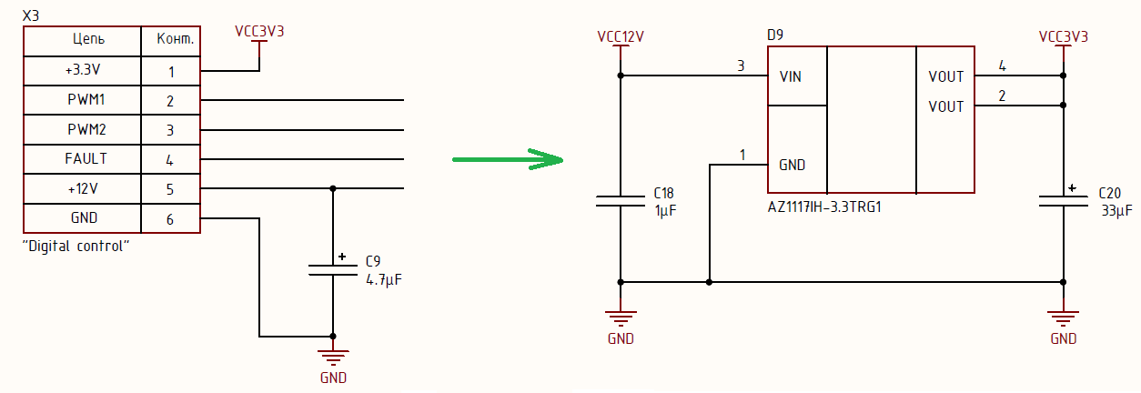
In the process of collecting the layout, I experienced a wild inconvenience from having to carry extra power + 3.3V to the power board. I don’t even know why I did it, I look at the circuit and I don’t understand myself)) In any case, it was decided to make the power supply for the module only 12V, and get 3.3V already on the board. The 3.3V bus current consumption is about 10 mA, it powers the logical part of transistor drivers, hardware protection logic and 1 LED, so it’s not economically feasible to install dc / dc and it was decided to use a conventional linear stabilizer (LDO):
The second revision of the design was also optimized for the cost of components. One of the key components that determines the characteristics of the module is the driver for power switches - 1EDC60I12AHXUMA1. This is the top driver from Infineon, but it turned out to be somewhat redundant, or rather, in this concept, it could not realize itself.
Yes, it has a high current of 6.8A for opening and 10A for closing, this allows switching a sufficiently large current at high frequency. In theory, cool, but in practice, I rested on the frequency limit caused by the parasitic parameters of the circuits and wires that connect to the module. The practical ceiling is somewhere around 250-300 kHz, and the most "popular" operating frequency range is about 60 ... 120 kHz, so it was decided to install a driver from the same line, but with a lower opening current and at the same time cheaper and available - 1EDC40I12AHXUMA1. It differs in general only by a smaller current, in practice the buck-converter and half-bridge with an operating frequency of up to 250 kHz were tested and this driver was enough to obtain optimal losses, which were approximately 15 ... 20% of the static on the channel. At the same time, this replacement allowed to reduce the cost by $ 6 only in one position! By the way, this driver is in DKO Electronics at a very good price, although 2 weeks ago they sold 200 pieces for 121 rubles, but they raked them quickly, I myself grabbed 50 pieces from greed.

Of course, you can leave the old driver, but in the Russian Federation it costs 2 times more, though it will reduce the total losses on transistors by about 5..10%. Or on layouts use 1EDC40I12AH, and in production to put the older brother 1EDC60I12AH, because the whole line of these drivers is pin-to-pin compatible.
The hardware current protection has undergone the deepest processing. The comments had a lot of valuableand not very good advice and questions, some of them were taken into account, the other part seemed irrelevant to me.
Here I would like to step aside a bit and tell you about the micro-experiment that was conducted in the first revision. As you remember, the simplest LTV-817 optocoupler (the same “popular” PC-817) was used to decouple the power unit from the control. It can often be found in the feedback (OS) of cheap pulsed power sources (SMPS), but there it is used in the OS for voltage, where special speed is not required. I wanted to try it in current protection hardware, because he has a nice price (about $ 0.03) and see in practice how he behaves. In principle, it copes with its task at frequencies up to 40 ... 60 kHz, with further increase in frequency, the optocoupler does not have time to switch (voltage rises slowly) and the through-current through the keys passes over 2-3 periods. Of course, with a short circuit current of 10-15A, this will only cause a slight heating and the protection will still work, but when powered from the network it is 100% broads - checked. I think the experiment was a success and PC817 can be put in defense if you make a high-volume device with a low switching frequency, where savings of $ 0.2-0.3 will be substantial.
As a result, I replaced this optocoupler with a fast, but more expensive and less popular - TLP2362, with it the reaction time of protection is 2 ... 6 μs.
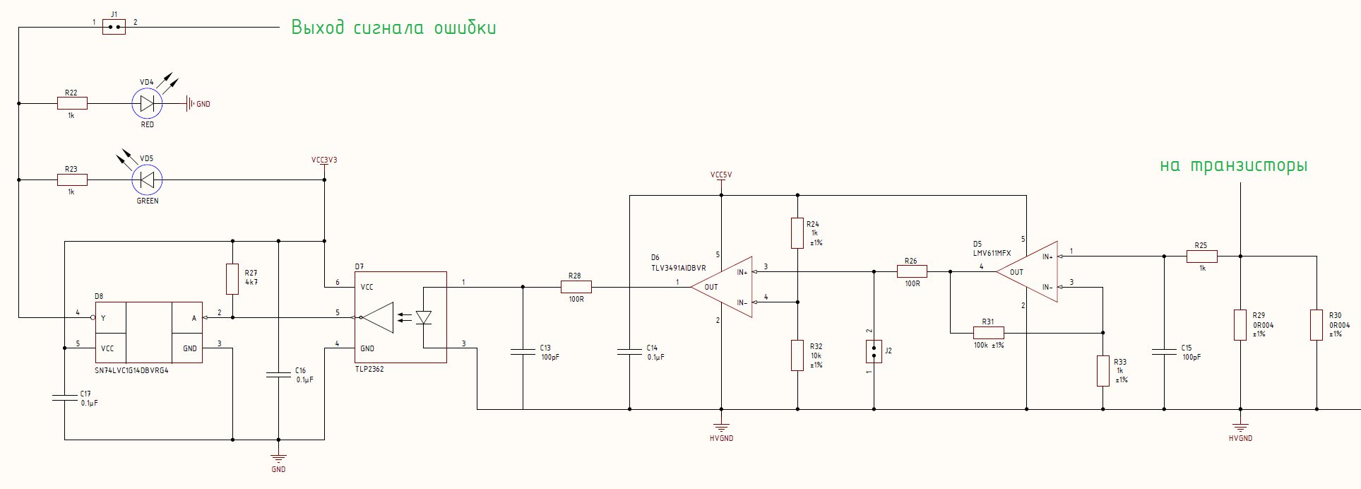
As you can see, the general ideology remains the same, the implementation and components have changed a little. As a current sensor, there are 2 parallel-connected shunt in a housing similar to 2512; in fact, these are 2 exact resistors with 1% accuracy, richer soldering sites and a power of dissipation of 3 W, they are produced by Bourns. In stores in the Russian Federation, they cost about $ 1-1.5, but I ordered 1000 pieces for LCSC, they probably bought the coil right away and the balance appeared on the site, the price is $ 0.05 or 20 times lower! Buy while in stock - link . Usually there are no such specific components on LCSC, but they appear only if someone has ordered a lot and the store has purchased them and sells the rest. Or you will need to order 100+ of these shunts and then bring them under you.
The signal from the current sensor is amplified by an operational amplifier (op amp) D5, which raises the voltage to 4V at 20A. Then, using the comparator D6, this signal is compared with the reference one and, if it is higher than it, then a logical 1 appears at the output D6 (pin 1), which “lights” the LED in the optocoupler. The optocoupler in this case has an inversion, that is, when log1 is fed to it, it outputs log.0 at the output, and to disable the D2 and D4 drivers, it is necessary to send log.1 to the outputs of 3, it turns out that the signal must be inverted back for what it is D8 inverter. We get that when an error occurs at the output of protection, the log.1 is set and the driver is turned off, and during normal operation, the output of the protection is log.0 and this allows the drivers to work normally.
Of course, it was possible to do without an inverter and implement a “pre-inversion” on the comparator, turning it on a little differently so that when the current is over, it outputs log.0, then the output of the optocoupler would be log.1 and the inverter D8 could be removed from the circuit. I did as I did to make the logic of the protection work more understandable to beginners, since This inclusion is the most obvious, and the inverter is essentially an additional current amplifier, which is important, because At the output of the error signal sits a LED, 2 driver chips and another microcontroller, or maybe you decide to hang something else, so the current margin here will not hurt.
Also, for the convenience of work, 2 jumpers were added. The first one (on the J1 circuit) serves to turn off the signal with current protection; by default, this jumper is closed and sends a signal to the driver and PWM controller / DSP. If for some reason you need to disable the protection signal or connect it to another circuit, then you can remove the jumper. The second one (on the J2 circuit) is simply the output of the amplified signal from the shunt, so that you can conveniently connect the oscilloscope probe or for the current operating system, although the galvanic isolation is “lost”.
In fact, this is a group of changes and it refers to a change in the layout and connectors. First, the connector for connecting to the control board is replaced from WF-6 to BH-10, since the latter allows you to more accurately draw the cable and for the assembly of the cable does not require soldering or tricky crimping. Secondly, the radiator was moved 1 mm away from the transistors, that is, by the thickness of the ceramic strip, since in the first revision this was not taken into account and the legs of the transistors had to be raped a little, which is not good. Third, the C7-C9 capacitors on the power bus were pushed another 1 mm away from the radiator; now the gap between the radiator and the capacitors is 3 mm.
The last change for me is not critical, because the radiator with a rated current of 20A was not heated by me above +65 o , but several people spoke about this potential problem, so it was decided to spend an extra millimeter of PCB.
It’s probably not a change, but just an alternative version - this time the high-voltage version of the module was also made. An IPP65R225C7XKSA1 transistor was used, C7-C9 capacitors were used in a similar 22x25 mm package with a capacity of 100 microfarads at 400V. You can also install only one shunt in the current protection circuit, then its resistance will be 4 mΩ, not 2 and, accordingly, the current cut-off will be 10A instead of 20.
Objectively, 20A in a high-voltage module is not squeezed, because the size of the radiator will not allow to dissipate so much heat, and at 10A they were successfully tested in a 3 kW model. Therefore, in the high-voltage module we put on 1 transistor, and choose the number of shunts by yourself. In principle, if the protection at 20A is configured, then it will also save from short-circuit, and with a significant starting current, it will not go crazy. Also, no one forbids in the high-voltage module to put on 2 keys up and down, the place has not gone anywhere.
The distance between the dc / dc module and the driver was also increased, and the module footprint was also fixed. The fact is that initially I took the model of the module case (SIP-7) from 3dcontent and did not check it, it turned out to be an error - the legs were 1 mm farther from the border of the case than in reality, therefore the module got into tightness. Now the model has been fixed and the gap is increased by 3 mm.
In the first revision, I worked out the basic concept of the module and the layout, the second revision changed the module somewhat, but not globally, so it was decided to order 50 boards at once, assemble a complete set and distribute several modules for testing repeatability and survivability incurved hands .

For myself, I assembled 5 modules: 2 low-voltage and 3 high-voltage. It was this set that I conceived of as a “developer kit”, since it allows you to assemble not just a separate converter, but also to mockup an entire device, for example, already tested fluently on a voltage stabilizer (3 high-voltage half-bridges), on the frequency changer, and now I am working on an inverter, which is 2 low-voltage modules for boosting 24V to + -380V a bridge circuit and one half bridge for a sine draper of bipolar voltage (I plan to write about it). Therefore, if you plan to thoroughly engage in the study of power electronics, then assemble the same kit, and for "try" it will be enough and one of course.

I ordered the boards on PCBway and there I got the following price tags:
Here in order 2 sets of boards, but it is clear that the modules themselves cost $ 64, that is, each board costs $ 1.28 / pc. Delivery costs $ 13 for everything, I think if you throw out the second set of boards, you could be able to meet $ 10 for delivery. The total cost of the boards was $ 1.48 / pcs. You can burn and not be upset))
Next time I plan to try ordering from the PCBway both the boards, the components, and the installation. It is interesting to see whether it will be possible to save up on the purchase of components. Unlike LCSC, PCBway itself is purchased on digikey, mouser and arrow (these distributors are more credible), respectively, you can buy everything all at once. In the same order, the transistors and drivers came from the Electronics Engineer, the rest from the LCSC is inconvenient and it is unprofitable to pay for 3 deliveries (fees + 2 component stores), you can save $ 20-30. If it is interesting, then according to this procedure and preparation of the documentation package I can write a “tutorial”.
Many asked about this in a personal and in the comments, I answered with a meaningful “later” and simply fought off by distributing the source code, which were attached at the end of the articles. Unfortunately for the first revision I was not 100% sure, so I asked to wait for it to run in and revision number two. “Revision number two” has arrived and I will describe various ways:
This time not only the scheme in pdf and gerber files is available to you, but also the original project in Altium Designer. You can make any changes or replace components, for example, suddenly you would like transistors in TO-247, put if you consider it necessary. There were a lot of suggestions and different tips in the comments, to objectively implement them all will not work, because they sometimes contradict each other and the time I don’t have a car at all, so you now have the opportunity to add all your Wishlist on your own and show everyone how to do it.
Alas, even in fairly simple devices, the 2nd revision of hardware is required in order to “clean up” the poor implementations of this or that functionality, improve the layout and constructive. As a result, work was carried out to optimize the technical parameters and to improve the usability of the module. Today in the article I will just tell you more about these changes, explain why this is the case, and at the end of the article you will see updated sources. Go!
')
Change No. 1
In the process of collecting the layout, I experienced a wild inconvenience from having to carry extra power + 3.3V to the power board. I don’t even know why I did it, I look at the circuit and I don’t understand myself)) In any case, it was decided to make the power supply for the module only 12V, and get 3.3V already on the board. The 3.3V bus current consumption is about 10 mA, it powers the logical part of transistor drivers, hardware protection logic and 1 LED, so it’s not economically feasible to install dc / dc and it was decided to use a conventional linear stabilizer (LDO):
Change No. 2
The second revision of the design was also optimized for the cost of components. One of the key components that determines the characteristics of the module is the driver for power switches - 1EDC60I12AHXUMA1. This is the top driver from Infineon, but it turned out to be somewhat redundant, or rather, in this concept, it could not realize itself.
Yes, it has a high current of 6.8A for opening and 10A for closing, this allows switching a sufficiently large current at high frequency. In theory, cool, but in practice, I rested on the frequency limit caused by the parasitic parameters of the circuits and wires that connect to the module. The practical ceiling is somewhere around 250-300 kHz, and the most "popular" operating frequency range is about 60 ... 120 kHz, so it was decided to install a driver from the same line, but with a lower opening current and at the same time cheaper and available - 1EDC40I12AHXUMA1. It differs in general only by a smaller current, in practice the buck-converter and half-bridge with an operating frequency of up to 250 kHz were tested and this driver was enough to obtain optimal losses, which were approximately 15 ... 20% of the static on the channel. At the same time, this replacement allowed to reduce the cost by $ 6 only in one position! By the way, this driver is in DKO Electronics at a very good price, although 2 weeks ago they sold 200 pieces for 121 rubles, but they raked them quickly, I myself grabbed 50 pieces from greed.
Of course, you can leave the old driver, but in the Russian Federation it costs 2 times more, though it will reduce the total losses on transistors by about 5..10%. Or on layouts use 1EDC40I12AH, and in production to put the older brother 1EDC60I12AH, because the whole line of these drivers is pin-to-pin compatible.
Change number 3
The hardware current protection has undergone the deepest processing. The comments had a lot of valuable
Here I would like to step aside a bit and tell you about the micro-experiment that was conducted in the first revision. As you remember, the simplest LTV-817 optocoupler (the same “popular” PC-817) was used to decouple the power unit from the control. It can often be found in the feedback (OS) of cheap pulsed power sources (SMPS), but there it is used in the OS for voltage, where special speed is not required. I wanted to try it in current protection hardware, because he has a nice price (about $ 0.03) and see in practice how he behaves. In principle, it copes with its task at frequencies up to 40 ... 60 kHz, with further increase in frequency, the optocoupler does not have time to switch (voltage rises slowly) and the through-current through the keys passes over 2-3 periods. Of course, with a short circuit current of 10-15A, this will only cause a slight heating and the protection will still work, but when powered from the network it is 100% broads - checked. I think the experiment was a success and PC817 can be put in defense if you make a high-volume device with a low switching frequency, where savings of $ 0.2-0.3 will be substantial.
As a result, I replaced this optocoupler with a fast, but more expensive and less popular - TLP2362, with it the reaction time of protection is 2 ... 6 μs.
As you can see, the general ideology remains the same, the implementation and components have changed a little. As a current sensor, there are 2 parallel-connected shunt in a housing similar to 2512; in fact, these are 2 exact resistors with 1% accuracy, richer soldering sites and a power of dissipation of 3 W, they are produced by Bourns. In stores in the Russian Federation, they cost about $ 1-1.5, but I ordered 1000 pieces for LCSC, they probably bought the coil right away and the balance appeared on the site, the price is $ 0.05 or 20 times lower! Buy while in stock - link . Usually there are no such specific components on LCSC, but they appear only if someone has ordered a lot and the store has purchased them and sells the rest. Or you will need to order 100+ of these shunts and then bring them under you.
The signal from the current sensor is amplified by an operational amplifier (op amp) D5, which raises the voltage to 4V at 20A. Then, using the comparator D6, this signal is compared with the reference one and, if it is higher than it, then a logical 1 appears at the output D6 (pin 1), which “lights” the LED in the optocoupler. The optocoupler in this case has an inversion, that is, when log1 is fed to it, it outputs log.0 at the output, and to disable the D2 and D4 drivers, it is necessary to send log.1 to the outputs of 3, it turns out that the signal must be inverted back for what it is D8 inverter. We get that when an error occurs at the output of protection, the log.1 is set and the driver is turned off, and during normal operation, the output of the protection is log.0 and this allows the drivers to work normally.
Of course, it was possible to do without an inverter and implement a “pre-inversion” on the comparator, turning it on a little differently so that when the current is over, it outputs log.0, then the output of the optocoupler would be log.1 and the inverter D8 could be removed from the circuit. I did as I did to make the logic of the protection work more understandable to beginners, since This inclusion is the most obvious, and the inverter is essentially an additional current amplifier, which is important, because At the output of the error signal sits a LED, 2 driver chips and another microcontroller, or maybe you decide to hang something else, so the current margin here will not hurt.
Also, for the convenience of work, 2 jumpers were added. The first one (on the J1 circuit) serves to turn off the signal with current protection; by default, this jumper is closed and sends a signal to the driver and PWM controller / DSP. If for some reason you need to disable the protection signal or connect it to another circuit, then you can remove the jumper. The second one (on the J2 circuit) is simply the output of the amplified signal from the shunt, so that you can conveniently connect the oscilloscope probe or for the current operating system, although the galvanic isolation is “lost”.
Change No. 4
In fact, this is a group of changes and it refers to a change in the layout and connectors. First, the connector for connecting to the control board is replaced from WF-6 to BH-10, since the latter allows you to more accurately draw the cable and for the assembly of the cable does not require soldering or tricky crimping. Secondly, the radiator was moved 1 mm away from the transistors, that is, by the thickness of the ceramic strip, since in the first revision this was not taken into account and the legs of the transistors had to be raped a little, which is not good. Third, the C7-C9 capacitors on the power bus were pushed another 1 mm away from the radiator; now the gap between the radiator and the capacitors is 3 mm.
The last change for me is not critical, because the radiator with a rated current of 20A was not heated by me above +65 o , but several people spoke about this potential problem, so it was decided to spend an extra millimeter of PCB.
Change No. 5
It’s probably not a change, but just an alternative version - this time the high-voltage version of the module was also made. An IPP65R225C7XKSA1 transistor was used, C7-C9 capacitors were used in a similar 22x25 mm package with a capacity of 100 microfarads at 400V. You can also install only one shunt in the current protection circuit, then its resistance will be 4 mΩ, not 2 and, accordingly, the current cut-off will be 10A instead of 20.
Objectively, 20A in a high-voltage module is not squeezed, because the size of the radiator will not allow to dissipate so much heat, and at 10A they were successfully tested in a 3 kW model. Therefore, in the high-voltage module we put on 1 transistor, and choose the number of shunts by yourself. In principle, if the protection at 20A is configured, then it will also save from short-circuit, and with a significant starting current, it will not go crazy. Also, no one forbids in the high-voltage module to put on 2 keys up and down, the place has not gone anywhere.
The distance between the dc / dc module and the driver was also increased, and the module footprint was also fixed. The fact is that initially I took the model of the module case (SIP-7) from 3dcontent and did not check it, it turned out to be an error - the legs were 1 mm farther from the border of the case than in reality, therefore the module got into tightness. Now the model has been fixed and the gap is increased by 3 mm.
PCB order
In the first revision, I worked out the basic concept of the module and the layout, the second revision changed the module somewhat, but not globally, so it was decided to order 50 boards at once, assemble a complete set and distribute several modules for testing repeatability and survivability in
For myself, I assembled 5 modules: 2 low-voltage and 3 high-voltage. It was this set that I conceived of as a “developer kit”, since it allows you to assemble not just a separate converter, but also to mockup an entire device, for example, already tested fluently on a voltage stabilizer (3 high-voltage half-bridges), on the frequency changer, and now I am working on an inverter, which is 2 low-voltage modules for boosting 24V to + -380V a bridge circuit and one half bridge for a sine draper of bipolar voltage (I plan to write about it). Therefore, if you plan to thoroughly engage in the study of power electronics, then assemble the same kit, and for "try" it will be enough and one of course.
I ordered the boards on PCBway and there I got the following price tags:
Here in order 2 sets of boards, but it is clear that the modules themselves cost $ 64, that is, each board costs $ 1.28 / pc. Delivery costs $ 13 for everything, I think if you throw out the second set of boards, you could be able to meet $ 10 for delivery. The total cost of the boards was $ 1.48 / pcs. You can burn and not be upset))
Next time I plan to try ordering from the PCBway both the boards, the components, and the installation. It is interesting to see whether it will be possible to save up on the purchase of components. Unlike LCSC, PCBway itself is purchased on digikey, mouser and arrow (these distributors are more credible), respectively, you can buy everything all at once. In the same order, the transistors and drivers came from the Electronics Engineer, the rest from the LCSC is inconvenient and it is unprofitable to pay for 3 deliveries (fees + 2 component stores), you can save $ 20-30. If it is interesting, then according to this procedure and preparation of the documentation package I can write a “tutorial”.
How to get paid?
Many asked about this in a personal and in the comments, I answered with a meaningful “later” and simply fought off by distributing the source code, which were attached at the end of the articles. Unfortunately for the first revision I was not 100% sure, so I asked to wait for it to run in and revision number two. “Revision number two” has arrived and I will describe various ways:
- Take the source in the form of Gerber-files and send it to your favorite manufacturer. Yes, I do not tie you to a specific production, everything is open and democratic. You may find prices lower or you may want to pay from the States, not China. If there are difficulties with the order somewhere, then you can also ask me, I will try to help;
- Order in one click on PCBway - order . The quality of the boards that you get can be seen in the photos in the article, the manufacturer also doesn’t exactly have any cuts inside the boards, and others had problems, they just didn’t make insulation cuts under the drivers and dc / dc modules;
- I have about 30 boards left, in principle, I can share them. The only request is that if you can order it yourself, then order, 5 boards cost $ 12 including delivery. If for some reason you can not order by yourself, then write - send you by mail.
Sources for the power module
This time not only the scheme in pdf and gerber files is available to you, but also the original project in Altium Designer. You can make any changes or replace components, for example, suddenly you would like transistors in TO-247, put if you consider it necessary. There were a lot of suggestions and different tips in the comments, to objectively implement them all will not work, because they sometimes contradict each other and the time I don’t have a car at all, so you now have the opportunity to add all your Wishlist on your own and show everyone how to do it.
Source: https://habr.com/ru/post/434658/
All Articles