UDB. What is it? Part 2. Datapath
We continue to consider UDB based on Cypress documentation. And this time we will examine in detail the Datapath, the operational automaton.
Previous article:
UDB. What is it? Part 1. Introduction. Pld.
21.3.2 Operational Machine (Datapath)
The datapath shown in Figure 21-6 contains an 8-bit single-ended ALU and its associated comparison and generation of condition flags. Datapath blocks of neighboring UDBs can be chained to increase the bit depth. Datapath includes a small dynamic configuration RAM that can dynamically select the operation to be performed in a specific loop.
')
Datapath is optimized for implementing typical embedded functions, such as timers, counters, PWMs, PRS, CRC, shift registers, and deadband generators. Adding addition and subtraction functions provides support for digital delta-sigma operations.
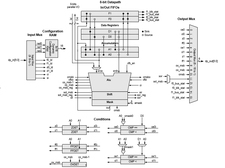
Figure 21-6. Top Level Datapath.
21.3.2.1 Overview
The following chapters provide an overview of the main features of Datapath.
Dynamic configuration
Dynamic configuration - the ability to change the work and internal communication Datapath in each cycle under the control of the sequencer. This is implemented using configuration memory (configuration RAM), which stores eight unique configurations. The input address of this memory can be forwarded from any block connected to tracing resources, usually from PLD logic, I / O pins, or from other Datapaths.
ALU
ALU can perform eight general-purpose functions: increment, decrement, add, subtract, and perform logical AND, OR, XOR, and PASS operations. The choice of functions is determined by the configuration memory for each cycle. Independent shift operations (left, right, nibble permutations), as well as mask overlay operations are available at the ALU output.
Conditional constructions
Each Datapath has two bitmasking comparators that can be configured to select a set of Datapath register inputs as arguments. Other detectable conditions can be all zeros, all ones and overflow. These conditions form the main outputs of the Datapath and can be thrown onto digital trace lines or the inputs of other functions.
Embedded CRC / PRS
Datapath has built-in support for one-cycle CRC computations and pseudo-random sequence generation (Pseudo Random Sequence, PRS) with given digits and a generating polynomial. To achieve a bit depth of more than 8 bits, the signals can be chained between Datapaths. This feature is dynamically controlled, which means it can alternate with other functions.
Custom high bit number
The number of the most significant bit (most signalized bit, MSB) of the arithmetic function and the shift function can be set programmatically. This provides support for variable length CRC / PRS functions, and, in conjunction with masking the ALU output, allows the implementation of arbitrary length timers, counters, and shift blocks.
FIFO input / output buffers
Each Datapath has two 4-byte FIFO buffers, each of which can be configured to work as an input buffer (CPU or DMA writes data to the FIFO, Datapath reads the FIFO), or as an output buffer (Datapath writes to the FIFO, and CPU or DMA reads from it). These FIFO buffers generate a status that can be forwarded to interact with sequencers, interrupts, or DMA requests.
Chaining
Datapath can be configured to chain conditions and signals in a chain with neighboring Datapaths. Shift, transfer, capture, and other conventional signals can be combined into chains to create arithmetic functions of higher capacity, as well as shift functions and CRC / PRS functions.
Time multiplexing
In oversampled applications, or where high clock speeds are not needed, one ALU in Datapath can be effectively divided between two sets of registers and condition generators. The ALU and shift register outputs are latched and can be used as input in subsequent cycles. Examples of use include support for 16-bit functions in a single (8-bit) Datapath or alternation of CRC generation operations with data shift operations.
Datapath Inputs
Datapath has four types of inputs: configuration, control, and data (serial and parallel) inputs. Configuration inputs select the address of the dynamic configuration RAM. Control inputs load data registers from the FIFO and dump the battery output to the FIFO. Serial data inputs include shift and transfer inputs. The parallel data input port allows you to receive up to 8 bits of data from trace resources.
Datapath Outputs
There are a total of 16 signals generated in the Datapath. Some of them are conditional signals (for example, comparisons), others are status signals (for example, FIFO status), and the rest are data signals (for example, shift register output). These 16 signals are multiplexed into 6 Datapath outputs and routed to a trace matrix. By default, the outputs are synchronized with a clock frequency, which creates pipelining with a delay of 1 clock. Also, their (outputs) can be switched to asynchronous (combinatorial) mode (see the translator's notes).
Translator's Note
I have been looking for a long time, what is the synchronism of the outputs Datapath. My experience said that everything is asynchronous. It turned out that what is meant is not so much the state of the outputs, as this is the setting of the editor for variables based on them.
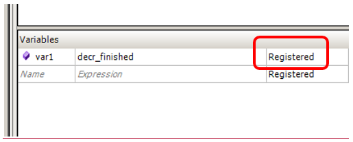
This will cause the editor to generate such Verilog code:
/* ==================== Assignment of Registered Variables ==================== */ always @ (posedge clock) begin : register_assignments var1 <= (decr_finished); end If you switch to combinatorial mode

the code will be like this:
assign var1 = (decr_finished); But all of this applies to variables generated from Datapath outputs. And the outputs themselves are always asynchronous. And their names (in this example, decr_finished ) can be used without entering additional variables.
Datapath Work Registers
Each Datapath module has six 8-bit working registers. CPU or DMA have read and write access to all registers.
Table 21-1
| Type of | Name | Description |
|---|---|---|
| Battery | A0, A1 | Batteries can be both source and receiver for ALU. They can also be loaded from the data register. or FIFO. Batteries usually contain the current value of the function. (e.g. counter, CRC or shear). These registers lose their values when going into sleep mode and when reset are taken value 0x00. |
| Data | D0, D1 | Data registers usually contain function constants. for example, a PWM comparison value, a timer period, or a CRC polynomial. These registers retain their values while in sleep mode. |
| FIFO | F0, F1 | Two 4-byte FIFO buffers are provided as the source, and receiver for buffered data. FIFO can be configured as input buffers and output buffers, or as one input buffer and one output buffer. Status signals show read and write status of these buffers. For examples of use include the buffered TX and RX data in SPI or UART, as well as buffered PWM data and buffered data about the period of the timer. These registers do not save their values. in sleep mode and when reset, take the value 0x00. |
In the next article we will begin to deal with the FIFO.
Source: https://habr.com/ru/post/433018/
All Articles