Development of buck-converter on STM32F334: principle of operation, calculations, prototyping
In my last two articles, I talked about the power module and the control board based on the STM32F334R8T6 microcontroller, which were created specifically to implement control systems for power converters and electric drives. An example of a DC / AC converter was also considered, which was a demonstration, not a complete construction. Now it's time to do something simple, but useful, and most importantly complete.
Most of the issues related to the project and power electronics are related to specific topologies: someone is interested in knowing the PFC control algorithm, someone wants to learn how to build a half-bridge LLC, but the most popular topology is undoubtedly buck. After all, a buck converter (also known as a buck converter) is the main one for most interesting projects: it is a driver for LED luminaires, and the basis of an MPPT controller for solar panels, and chargers, and much more.
There is a lot of information on the buck in the network, including datasheets, but it is scattered and I personally haven’t met any material that describes in detail the process of creating a digital-controlled buck converter. It's time to fix it. There is practically no mathematics, an explanation “on the fingers”, so it will be interesting to anyone who is somehow connected with electronics.
')
First you need to understand what we want to get in the end and what kind of input we have. The buck topology is downward, that is, it allows you to build a downward voltage converter. As you will see below, the voltage at the output of the buck-converter is almost linearly dependent on the input voltage, so you need to add feedback. Today I will talk about simple voltage feedback (voltage mode), which is the most obvious and will allow you to understand the principle of operation, and you will have enough of such feedback for most tasks.
At the end of the article we will get a working stabilized voltage source in the “synchronous buck” topology, operating at a sufficiently high frequency with digital control, implemented on the STM32F334R8T6 using the High Resolution PWM (HRPWM). The input voltage range is 15 ... 60V, the output voltage is 12V, the maximum output current is 2A.
I will begin to tell from the very basics and will gradually improve our converter, since “Synchronous buck” is an improved version with increased efficiency and control complexity. The basic topology, which you probably used, is as follows:
This topology is used in low-power voltage converters, for example, to power digital circuits and other low-power devices. The dc / dc downgrades that you use in your devices are most likely implemented on microchips for this topology. An example of such a chip LMR16006 .
The principle of operation of this circuit is very simple, the PWM signal is sent to the VT1 transistor, the work itself is divided into 2 stages, which alternate one after another:
When I got acquainted with this topology at 6-7m class, I didn’t understand right away why the diode does not conduct current at the 1st stage, now it seems trivial, but I think it is worth mentioning. When VT1 is open, a + VIN potential is applied to the cathode of the VD1 diode, for example, + 20V, and a ground potential is applied to the diode anode. In order for the current to flow through the diode it should be exactly the opposite: the potential at the anode must be greater than the potential at the cathode, therefore, in a buck, the diode is “closed” at the energy accumulation stage. At the stage of discharge, the diode already closes the circuit, the potential + VIN does not act on its cathode and does not “lock” it. I hope clearly explained.
Here you should have a question: “And what voltage will be at the output, if we applied to the input 20V?”. As always, everything is simple:

As can be seen from the formula, the output voltage linearly depends on the duty cycle (duty) of the PWM signal, which we apply to the VT1 transistor. If someone does not know or has forgotten the “duty ratio” is the ratio of the time that the transistor is in the open state to the period duration. This ratio can take a value from 0 to 1 or from 0 to 100%. Then we will operate with this particular figure when controlling the converter, but for understanding the essence let's substitute this relation into the formula:
The frequency of the buck-converter value is constant and is selected when designing, during operation it does not change, and therefore the period (T) is constant. It turns out that the output voltage directly depends on two physical quantities:
I think you have started to see the overall picture and the principle of work, let's fix it now and look at the real oscillograms and check this ratio in practice. I have assembled a buck model, which is loaded with a 10W LED. I used 3 oscilloscope channels, which are included in the following points:

Test №1 - Input voltage (Vin) constant 20V, changing the fill factor
As you can see on the oscillograms, the relation between the output voltage and the fill factor is correct. Of course, this was an “idealized” experiment; in reality, the input voltage is not stable and floats in a fairly wide range. Let's now see what will be the dependence on the input voltage with a fixed filling.
Test No 2 - The input voltage (Vin) changes, the fill factor is constant and is 50%.
Now we are convinced in practice that the output voltage also linearly depends on the input voltage with a fixed fill factor. Understand how to stabilize the output? The principle of stabilization is simple as the formula itself - Vout is 12V and a constant, we can change the fill factor using a microcontroller, so if Vin increases, then the output voltage increases and at this point we decrease the fill factor (duty) again until 12V. Accordingly, with a decrease in Vin, we begin to increase the fill factor until, again, the voltage Vout becomes 12V.
What else would you like to pay attention to in the theoretical section ... Oh, yes! Surely you wonder how PWM with an amplitude of 20V after the transistor eventually turned into a constant voltage with scanty pulsations? Indeed, if we put the red probe of the oscilloscope at the source of the transistor VT1, the green probe after the LC filter, we will see the following picture:
You can see how the LC-filter "lubricates" the alternating voltage into a constant, but the point is that the energy stored in the inductance and capacitance cannot be instantly consumed, hence the voltage cannot instantly change. We get that at the moment when the PWM before the choke is 0V, the output voltage is provided by the energy stored in the filter, which does not dissolve instantly and is enough to maintain the voltage at the time of closing VT1. This is all on the fingers of course, if it is interesting to go deeper, then as always I advise you to start the book B.Yu. Semenova "Power electronics: from simple to complex" , there is a whole chapter on the buck (chopper).
As I wrote a little earlier - it was a basic version of the topology. Its main disadvantage is high losses on the blocking diode. What current in the simple systems working on MK and CPLD? Usually within 1A, sometimes 2A, if there is some TFT display. In this case, the loss even when using a Schottky diode will be 0.4V * 2A = 0.8W. In principle, it is tolerable, it is possible to dissipate so much on the SMA / SMB case without problems, although at a voltage of 3.3V and 2A a loss of 0.8V is still 12% efficiency!
Now imagine a case where the current is 20A. It could be an MPPT controller, a large FPGA power system and much more. In this case, the loss will be 0.4V * 20A = 8 W! What does it mean? For example, in the case of MPPT, you will have less energy stored in the battery, in the case of powering the FPGA it will be an additional 8 W of heat that needs to be dissipated somewhere and in both cases it is undoubtedly a loss of overall efficiency. What can be done? And let's replace the VD1 diode with another N-channel Mosfet and get the following circuit:
Now the transistor VT2 acts as a diode, that is, conducts a current when VT1 is closed. The diode, which was in the basic version did not require control, but now we have to pay for an improvement in performance with an additional control channel with a PWM signal.
First, let's calculate how much we have reduced losses. The resistance of the channel of the modern mosfet is a few mΩ. As an example, let's take a transistor from my power module, which I described in previous articles - IPP083N10N5AKSA1 with a channel resistance of 8.3 megohms. We get static losses equal to 0.0083 * 20A * 20A = 3.32 W. Of course, there will also be dynamic losses, which with an adequately designed driver will be no more than 20%, that is, the total losses will be 4W. We get that the transition from the usual buck-to synchronous allows halving the losses on the diode.
Let us now analyze the complicated management. As we already understood, the blocking diode conducted the current when VT1 was closed. From this it follows that VT2 must be closed when VT1 is open and, accordingly, VT2 is open when VT1 is closed. If it is simpler, the transistors work alternately: or one is open or the other, if both transistors open, a through current will arise, since they are closed between themselves VIN and GND. Let's see what should be the signal, where the “yellow channel” is a VT1 transistor and the “green channel” is a VT2 transistor:

As you can see, if the logical channel “1” is set in the yellow channel (on VT1), then at that time a logical “0” should be set in the green channel (on VT2). We obtain that VT1 pumps energy into the LC filter, and VT2 closes the circuit at the stage of discharge.
There is one more thing about which you have already heard or read above - through - through current . The fact is that a real, not an ideal transistor (mosfet) has a certain capacity on the gate, that is, in reality, it does not instantly go from log.0 to log.1, and the energy in the transistor does not dissolve instantly, resulting in transistors for a short time at the moment of switching may both be open. This can lead in the best case to increased losses, which means heating up and in the worst case to the woman, since Through current is a common short circuit (short circuit). To avoid this, between turning off one transistor and turning on another, a delay, or so-called dead-time, is introduced. It looks like this:
I think you noticed that there is a small space on the signal switching edge. I installed it obviously large (about 3%) so that you can see it, in reality it is much smaller. In general, dead-time (further dt) is set as short as possible, but at the same time sufficient for the transistors to close. It can be calculated, or it can be chosen empirically, I personally think that this and that option is normal, but bearded Jedi will surely tell you: “It must be considered necessary, but it is better to simulate!”. This is certainly correct, but decide for yourself - if you are not too lazy to model in LTspice taking into account the parasitic inductances and capacitances of conductors and components.
For the stand in this article, I set the dt to ~ 100 ns (actually 104). My module allows you to install it significantly less, because The driver is very harshly applied, but surely many of you will assemble your layout without my module, which means there will most likely be snot there. I’ll leave dt with a margin so that I don’t bang because of the snot, and if you have a normal layout on the board, then you can reduce it yourself - then in the chapter on the code you will see how, but in the meantime we’re actually looking at dt:
Here you can see that dt lasts 2.5 divisions and each division is 40 ns - it means that the duration is ~ 100 ns as intended. I hope you understand why dt is needed, how long it should be, and how the buck topology works in general. If you do not understand, then as usual the questions in the comments, HP and the mail are accepted, while I seem to be answering everything.
In this part of the article, I will show how to quickly and simply calculate the main power components for a synchronous buck-converter, namely: choke, input and output capacitors, transistors.
I recall the introductory data:
Output voltage 12V is selected because As a load, I plan to use a 12V 20W LED, which is at hand and is a very visual load. Anticipating the questions of the “experts” in the comments - yes, I am aware that the LED needs current stabilization, but we do a voltage regulator and the LED is just a load.
The input voltage is chosen from the bald, you can do 15 ... 60V, so if you are interested in a different range, you can calculate the value of the components for it. A rated current of 2A is chosen to obtain an output power of 12V * 2A = 24 W, that is, slightly more than is needed for the LED. The LED itself at 12V consumes about 1.82 ... 1.9A.
The most interesting parameter remained - the operating frequency of the converter. What should it be? Here you have to answer yourself, in my case it is 100 kHz. The choice is based on two theses:
Now I will not talk about the choice of frequency, just accept that 100 kHz. After I show the calculation method, we will return to this question, because the formulas will more clearly show the dependence of the denominations of the main components of the operating frequency.
Step 1. Select transistors
We will be mainly interested in 3 parameters: maximum drain-source voltage, channel resistance in the open state and gate capacitance. The entire potential of the voltage source (Vin) is applied to the transistor, and there are also spikes at the moment of switching. You have 2 options: take the transistor VT1 and VT2 with a voltage margin or the story RC snubber at VT2. In my case, there are 100V transistors on the power module, and with an input 30V, this is a huge voltage margin, even 60V was enough to do without snubber and protect the transistor from breakdown.
Channel resistance - here the less, the better, but there is one BUT. With a decrease in channel resistance, we reduce static losses (I 2 * R), but the technology is such that the capacity of the shutter increases, and this leads to an increase in dynamic losses. You have to find a middle ground between the "channel resistance" and "gate capacity". For voltages up to 100V, I advise you to pay attention to Infineon's OptiMOS series transistors; you can already look at high voltages for parametric search or even towards IGBT transistors. The latter are also supported by my power module and do not require any changes in the driver.
Step 2. Calculate the inductor inductance
It is necessary to calculate the minimum value of inductance, which will allow our dc / dc converter to work in the continuous current mode (L min ):

For variables, I think everything is clear, except - k ind . These are permissible ripple currents in the choke, usually choose the value of 20 ... 50%, but I almost always set 30%. The smaller the ripple of current, the further we will be from the saturation limit of the core on which the choke is wound, but as can be seen from the formula, we need a large inductance of the choke.
Now we calculate the minimum value of inductance, which is needed for my input data, ripple, I will lay 30% as already written above:

It should be understood that this is the minimum inductance required for the buck-converter to operate in the continuous current mode, but again there is a nuance. In the process of increasing the current acting in the winding, the permeability of the core and the inductance of the choke WITHOUT current and With the current are slightly different, somewhat different for different materials. In order to avoid the situation when the inductance decreased below L min and the dc / dc did not go into the discontinuous current mode when the current increased in the inductor, it is necessary to slightly increase the inductance, that is, add a couple of extra turns during the winding. Increasing the inductance by 10-15% will be enough for the material Kool Mu, and my choke will be on it.
Step 3. Calculation and manufacture of the throttle
I wanted to describe this procedure in the “prototyping” section, but then the inductance calculation stage would have remained less clear for you, and probably missed the interesting pictures, so I’ll describe everything here. For the manufacture of the throttle, I will take the throttle R26 / 14/11 (R is a ring, and the numbers are dimensions) from the material Kool Mu with permeability 60, download the documentation on it and you can buy it here - Lepkos .
Now you need to count how many turns and which wire to wind. Let's start with the number of turns perhaps. In the documentation on the core there is such a convenient parameter - A L , which is equal to 75 nH / revolution 2 . Here carefully - the turns in the square! To find the inductance of the core, you must multiply A L by the number of turns in the square. Hence, the formula for finding the number of turns looks like this:

In order to obtain the minimum required inductance, it is necessary to wind 40 turns, but as we have already discussed, it is necessary to slightly increase the inductance, say, throw +3 turns. Take the ring and wind 43 turns, we get the following choke:

Now for the sake of interest let's calculate what inductance should be:
And for reliability, we check the inductance of the choke with tweezers:
137 μH, great! The results agreed, the error is within ± 8% for A L. Here it is worth noting - if you do not have the ability to measure inductance, then do not buy cores for aliexpress, in ChiD, complex, electronic engineer and other “eatery” - there is a chance to get a core from another material or not that permeability, but with proper marking - verified. Without the ability to measure inductance, you will not be able to test A L and you will be able to spend a lot of time searching for the cause of the “broadshaft” of your converter.
Then a reasonable question will appear - “will we have enough of the core and its dimensions? Maybe it was necessary more? ". For the material Kool Mu, the magnetic induction limit is 0.5 T, in practice it is better not to climb over the threshold above 0.45 T without obvious need. It turns out that the winding wound on the core does not have to create an induction at each point of the core more than 0.45 T, so check:
As you can see, the value of magnetic induction 0.06 T is much lower than the limit 0.5 T. Two conclusions can be drawn from this: firstly, the throttle will not go into saturation, and secondly, the core is very large and powerfully take a ring of substantially smaller size. I took the ring R26 simply because I have a whole box of them, there is no other secret meaning here.
It remains to determine what wire size to take for the choke. Firstly, I strongly advise you not to take a wire with a diameter of more than 1 ... 1.2 mm at such high frequencies, since The skin effect already has a significant effect and reduces the effective cross section. Secondly, the current density in the wire must be selected based on the conditions of cooling and power. At low powers (up to 10–20 W), it is possible to safely lay a current density of 8. 10 A / mm 2 even without airflow. At powers up to several kilowatts, it is better to lay the current density in the range of 5 ... 6 A / mm 2 , and at powers from 10 kW and further it will be reasonable to reduce the current density to 3 ... 4 A / mm 2 .
I had a varnished wire with a diameter of 0.8 mm on hand. Its cross section, respectively, is ~ 0.5 mm 2 . At a current of 2A, we obtain a current density in the winding of about 4 A / mm 2 . I could use a wire and half the size of the cross section, but my core is large enough, so the wire of a larger cross section got in without problems. When you optimize your device, you will have to first read and then buy the wire of the desired cross section, then you will be able to get the optimal dimensions of the choke.
Step 4. Calculate the output capacitor
At this stage, as in the case of inductance, we will consider the minimum value of the capacitance, which must be installed in the LC filter at the output of the buck converter. Accordingly, if you install more, it will be better and then you will see why. Calculate capacity:
Of course, the capacity must also be set with a certain margin, especially if you use only ceramics at the outlet, since its capacity is greatly reduced depending on the voltage applied to it. You should also pay attention to the dependence on pulsations - the variable V pulse . This is the maximum value of the ripple at the output, that is, ideally with a capacity of 147.8 microfarads, the amplitude of the ripple will be 0.2 V, that is, the output voltage will float in the range of 11.9 ... 12.1 V. Want to reduce ripple? Then reduce them in the formula and the value of the resulting capacity will increase accordingly, of course, you will not get a laboratory power supply simply by increasing the output capacity. It is also necessary to take into account the need for a low ESR, for this purpose, 1-2 electrolytes are usually put in parallel and in parallel they are hung with ceramics a few microfarads with the X7R dielectric desirable. If the budget allows, then you can replace the electrolytic capacitor with polymer tantalum (as in a GPU) and so ceramics are not needed, they have an ESR and so little.
Frequency considerations
Now, as I said, let us return to the question of choosing the operating frequency of the converter. Let me divide the conclusions into several thoughts:
I think from these theses it became clear to you what the switching frequency affects, now you need to independently learn how to find the "middle ground" between losses on transistors and the size of the device. In one of the following articles I will teach you how to optimize the working frequency for maximum efficiency, the main thing is not to forget that I was going to do it.
So, the most tedious, but important, part is over, now the hardware and code will go. Let's put together a model on which we will implement theoretical calculations. To do this, we need two modules about which I described in previous articles: the power module and the control module on the STM32F334 . You can also collect a half-bridge from any IR2110 waste trap yourself on the breadboard, and use any MC: STM32-Discovery, LaunchPad, Arduino and simply adapt the operation logic and code to your favorite MC; nothing will be difficult if You understood from the first two chapters how the buck converter works.
Now, let's make our structural diagram of the buck more “realistic” by adding the nominal values of all the components to it and correctly reflect the number of capacitors, as well as what part my power module can implement:
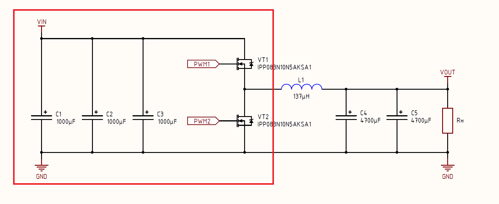
As can be seen from the diagram, the module already contains a half bridge (two transistors) for the implementation of a synchronous buck and input capacitor. By the way, the module has a huge margin in the module - there are 3 electrolytes of 1000 µF each and 100V, which is enough to build a buck for 500 -800 watts. It remains for us to add a choke, which we have already manufactured and output capacitors, the latter, too, by the way, with a margin, since I found only 4700 microfarads of 25V for low voltage, but they are some kind of Chinese, so I also decided to pair a couple. In fact, 470 uF of one is enough, but I simply didn’t have such little things in the hatchet. It turns out this design:
As previously mentioned, a high power 20W LED is used as a load. I don’t know how much he is shining, and it’s not very interesting, but at 12V it consumes just 21 ... 22 W, which is what my buck converter is designed for. The LED itself smeared KPT-8 and screwed it to the radiator, it is of course not enough, but it lasts 5-7 minutes of operation without problems (heats up to +40 ... 50 o C), and I don’t need more. We connect from the control module 2 signals HRPWM, GND and through the divider we catch the output of the buck to the ADC, as a result we have the following stand:

Now we have everything we need to start writing code and liven up our buck converter. First, let's look at the pin-out for the STM32F334R8T6 microcontroller, which stands in the control module:
Now we understand what the microcontroller pins will be used. On the module itself, I will need only 1 of 5 channels to control the power section; we will use channel “A”. This channel, like the others, has 2 high-precision PWM outputs (HRPWM), 1 error input (we don’t use it), GND for combining the ground of the boards and 2 ADC channels (we’ll use only one for voltage).
A little bit about HRPWM
In the open spaces of the Russian-speaking segment of the Internet, I practically did not encounter any training materials on HRPWM and did not meet at all materials on working with HRPWM based on STM32 microcontrollers, and this is a very useful peripheral.
In this article I will not delve into the theory of this periphery, so I will describe the essence. HRPWM or High Resolution PWM is a PWM module that is familiar to us, which has a higher resolution setting of the duty ratio and, in addition, usually has more flexible settings.
And this is only a small part of the features, on the HRPWM device diagram you can still see the possibility of synchronization with a bunch of events, DACs, built-in comparators to the MC, and alongside this flowchart there are many more documented features.
There remains the last question that needs to be addressed - “why is this PWM high-bit?”. To do this, consider a simple example. Imagine that you decided to use the MK without HRPWM, say STM32F103C8T6, which also operates at 72 MHz. We need to control a half bridge at a frequency of 70 kHz, which step of regulation we can get: 72,000,000 / 1025 steps = 70,243 Hz. Yeah, we have 1025 steps and when adjusting we can change the output voltage with a theoretical step of 1/1025 = ~ 0.1%. Now we take STM32F334, with a clocking frequency of 144 MHz and a timer shift depth of 32 bits, we get the equivalent frequency of 144 MHz * 32 = 4.608 GHz. For those who are frightened and questioned in the figure:

No, this is not the operating frequency, this is the equivalent frequency. What does this give us? We take the equivalent frequency of 4,608,000,000 Hz / 70,300 Hz = 65,535 steps. Now we can adjust the voltage (or current) at the output in 1/65 535 increments = ~ 0.001%, that is, 100 times more accurate!
And now let's do it - the frequency is 700 kHz, which is normal for a multi-phase buck, for example. F103 will have 72 000 000 Hz / 700 000 Hz = 102 steps, which allows at best to get a regulation of 1%, but this is 1% for duty, that is, in reality, with so many steps you will have voltage to float at the output as if stabilizing and no special. Whereas for F334 the number of steps will be approximately 6500, which still allows you to build a very accurate voltage or current regulator. We get that the resolution (step) of the setting of the duty ratio is much higher / more often than that of a conventional MK with a standard PWM module inside.
Setting up the clocking system
As a development environment in this article, I used TrueSTUDIO, because it is free, not as poor as Keil or IARyes yes, tell me about his wonderful debugger , cross-platform and perhaps the best solution for beginners and not only. At the end of the article there will be an archive with the project for this particular IDE. I will not tell you how to create and customize a project, just leave a link to the video, where everything is shown in detail - look .
After the project has been created and the LED has flashed, it is necessary to adjust the clocking system, namely from 8 MHz, raise the frequency to 72 MHz and feed it to the core, and then adjust the divider to reduce the frequency applied to the ADC:
Everything is simple, I think, the setup algorithm is as follows: goes to external quartz (HSE) -> wait for the transition to complete and set the ready flag -> send the PLL signal from the quartz to the input -> multiply 8 MHz by 9 -> 72 MHz, divide by 10 to clock the ADC -> turn on the PLL -> wait until it turns on and sets the ready flag -> feed the system bus and the core with the PLL -> wait until the switch is completed -> ready.
HRPWM Setup
Here everything is somewhat more complicated. There is a lot of functionality for this module, a lot of configurations and the amount of documentation is very large, but this is a minus and at the same time a plus - you have to pay for flexibility.
It is necessary to indicate that HRTIM is clocked from the PLL, the multiplier x2 is already on by default. Then we just turn on clocking for HRTIM, here is the first feature - as we understand the timer is clocked by PLL, but turned on for APB2. This is not entirely logical, but in a file with CMSIS it is easy to search or in the documentation.
PA8 and PA9 is the output of Timer A, which on my module goes to channel No. 1, which you can see on the diagram and pin-out. The legs are configured as a push-pull with an alternative function, the number of the function for both legs is the 13th. It is also important to tune to the maximum GPIO frequency, otherwise it will be an incomprehensible blockage of the front and the fall of the signal, which is extremely critical for power electronics.
Before you start, you need to calibrate the timer, because it works with minimal delays, then just wait for the ready flag.
That went flexibility. Firstly, we can set our own frequency for each timer A ... E, then we simply record the period of our PWM. Secondly, by default we have the PIMA alignment at the beginning of the period, that is, the signal goes to log.1 at the beginning of the new period, and now we need to choose when it returns to log.0, in this case by comparator No. 1, that is I ask in it the essence of the fill factor (duty).
For example, you can translate PWM not at the beginning of the period, but by comparator # 1, but return to log.0 by comparator # 2 and thus move the phase by hardware.
At this stage, we include the dead-time and set it up, in principle there are all the formulas in the comments, they can also be found in the reference manual. DT with a duration of ~ 100 ns you have already seen on the oscillogram in the theoretical chapter of this article. Dead time can be set separately on the front and on the decline of the signal. By the way, [0] is Timer A, respectively [1] is Timer B and so on.
For me it was not the most obvious point. Essentially, I want to make it so that at 10% of the duration of the Timer A period, an event is generated that would trigger the ADC conversion and measure the feedback signal. Why 10%? Just ideally, the measurement should not occur at the time of the transition of PIM from 0 to 1 or vice versa, because at this moment transients and disturbances occur in the power section, and we do not need to measure them. Therefore, in my case, 10% is optimal, since at 12V output and 30V input voltage of the duty cycle (duty) does not fall to 10% and the switching time of the transistor does not exactly coincide with the measurement of the ADC.
Now we need to look at the event communication system between HRTIM and the ADC:

In the first line, we choose exactly when the comparator will work, in my case it is 10% of the period of timer A. Next, we select a specific trigger in the ADC that MK will contact, 1 or 3 is available. Now it simply indicates which event will send a signal to the ADC, in my case it is comparator # 2.
And the final chord! We allow HRTIM to output signals from Timer A to our GPIO. Now we select the mode, it can be infinite (I have it), and it happens that the timer is turned on for 1 period and after that it must be started again. Next, set the period for the Master timer and turn it on with the last step, it starts clocking the channel timers and the PWM signal appears at the output.
It was a setup function, it remains to make a function that will set the fill factor (duty), it is with it that we will work when creating the regulator:
Now let's find out if we are going the right way. In the main function, we initialize the HRTIM setting and set the duty cycle, say 22500. With an input voltage of 20V and a period of 45000, our fill factor will be 50% and the output will be about 10V. This is not enough to blow up the LED to the full, but it should catch fire and we will understand if the power part is working, is everything good with dt and so on. I started everything from the first time:
You can see that all previous theoretical calculations have been confirmed. With a fixed duty cycle (duty) of 50%, the output voltage was simply divided into 2: 20V -> 10V, 22V -> 11V, 18V -> 9V. Now let's make it so that the voltage at the output is stable and does not depend on the input, that is, we add feedback.
Setting ADC and regulator
About ADC in STM32 a lot has already been written to me, I elaborated on only setting up a trigger tied to the HRTIM comparator. I will briefly tell you about the rest of the ADC settings. We look at the initialization function:
I use the regular channel mode, I have only one channel and it is selected in the SQR1 register. Enabled the ADC number 2, namely, its input IN5, it is fast and can operate at the maximum sampling frequency, but not this time. The sampling rate is equal to the PWM frequency, since 1 period = 1 sample, in principle, this is more than enough.
We also need to select an event in the CFGR register that will trigger the conversion, that is, Event 7 , why exactly? Look in RM:
Trigger 1 from the HRPWM module comes to Event 7 for our ADC No. 2, which in this case works as a slave, it is controlled from the HRPWM module. I think now it is clear how to connect 2 modules, in principle, the algorithm is similar for any periphery and any timer, except the register name will be different.
Upon reaching the period counter, the master timer will start the conversion, which after about 15 cycles (how many exactly look at RM-e) will cause an interrupt and you can pick up the result. It is in this interruption that we organize the control algorithm. Yes, it’s better not to do something massively inside the interrupt, it’s better to set the flag and transfer the execution further, but I allow myself this simplification, because in this case my controller is not particularly loaded and it will be able to calculate and exit the interrupt with 146% probability the appearance of a new one.
Little about management
Imagine that you entered the bathroom and decided to wash your hands in the sink. You slightly open the water, touch with your hand, cold? Add more hot water, warmer? Good! Add more hot water? Almost what you want? Good! Add more hot water, try with your hand, burn it? Come on now, let’s cool down a little. Good? And so indefinitely you will turn the tap until the water temperature is perfect. This is the easiest regulator!
Only in our country it is not the amount of hot water that is regulated, but the fill factor of PIM. Instead of a hand, we have an ADC with measured result. It remains only to implement the logic. We will calculate that we must issue an ADC at 12V at the output, and then using the if condition, we force our controller to support this value by changing the fill factor (duty).
To begin with, let's hang up a voltage divider on the output in order to reduce 12V to 2-2.5V, for example, since The ADC can measure from 0 to + 3.3V, and if you apply 12V, the microcontroller will burn simply. Therefore, I will put a divider with nominal values of 10 kΩ and 2 kΩ, which will give a division factor of 6 and, accordingly, our + 12V will turn into + 2V. Our ADC will produce the result: adcResult = (V out / k) / V ref * 2 12 = (12V / 6) / 3.3 * 4095 = 2481. Now we write the code for the interrupt handler:
The first thing after getting into the interrupt handler is to reset the flag of the interrupt itself, otherwise the second time you will not get into it. Then we read the result and save it as adcResult variable. Now, knowing the voltage at the output, you need to make an adjustment to the value of the fill factor for PWM, I realized this simply through the if condition. In each PWM period, we measure, increase or decrease the fill factor and set the result for the next period. Everything is simple, fast and visible essence. We look at the result of the work:
As you can see, everything works and when the input voltage changes, the output itself remains stable at 12V. Strongly attentive can notice small needles skipping, then you just need to hang up the X7R ceramics at the output of 1-10 microfarads and they will leave, I'm just too lazy to look for it and solder it. Now the oscillogram itself, so as not to spoil the eyes:

Here you can see how the output voltage rises. The fact is that due to the control algorithm, the filling must reach values from 0 to 10,000, for example, a thousand periods are needed, or approximately 10 ms. It suits me because soft-start, if you want to shorten the rise time, then just complicate the algorithm and add +1000, not +10, and the closer you get to the specified 12V, the less regulation step you take until you reach +10 . In general, in terms of management, you can do a lot of things, so you have a field for experiments.
Another interesting point is the oscillations at the moment of shutdown, such an "accordion". The fact is that after turning off the power, my digital part continues to work from another power supply unit and it tries to keep the desired value at the output. Where does energy come from? Yes, from the input capacitor, these are those that are 1000 microfarads each, as many as 3 pieces, this is such an interesting phenomenon.
The article came out is not small, but you wanted everything and immediately say, let's get a finished piece of metal - you will get it. I hope you enjoy the article, tried to make it more likely not scientific, but popular science, so that the material was available to people with different levels of knowledge and experience. Perhaps in the future I will analyze similarly other topologies like boost, full bridge and others.
By the way, this article and code will serve for the new MPPT controller at 20A, which I am designing. Now I am waiting for PCBway boards , which, in fact , volunteered to sponsor my open source projects with printed circuit boards, the source code for MPPT will also be open to all my modules.
Most importantly forgot! Keep the project with the code for TrueSTDIO - RAR .
Most of the issues related to the project and power electronics are related to specific topologies: someone is interested in knowing the PFC control algorithm, someone wants to learn how to build a half-bridge LLC, but the most popular topology is undoubtedly buck. After all, a buck converter (also known as a buck converter) is the main one for most interesting projects: it is a driver for LED luminaires, and the basis of an MPPT controller for solar panels, and chargers, and much more.
There is a lot of information on the buck in the network, including datasheets, but it is scattered and I personally haven’t met any material that describes in detail the process of creating a digital-controlled buck converter. It's time to fix it. There is practically no mathematics, an explanation “on the fingers”, so it will be interesting to anyone who is somehow connected with electronics.
')
Introduction
First you need to understand what we want to get in the end and what kind of input we have. The buck topology is downward, that is, it allows you to build a downward voltage converter. As you will see below, the voltage at the output of the buck-converter is almost linearly dependent on the input voltage, so you need to add feedback. Today I will talk about simple voltage feedback (voltage mode), which is the most obvious and will allow you to understand the principle of operation, and you will have enough of such feedback for most tasks.
At the end of the article we will get a working stabilized voltage source in the “synchronous buck” topology, operating at a sufficiently high frequency with digital control, implemented on the STM32F334R8T6 using the High Resolution PWM (HRPWM). The input voltage range is 15 ... 60V, the output voltage is 12V, the maximum output current is 2A.
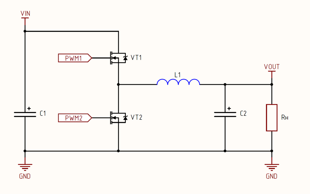
Chapter 1. The principle of the buck topology
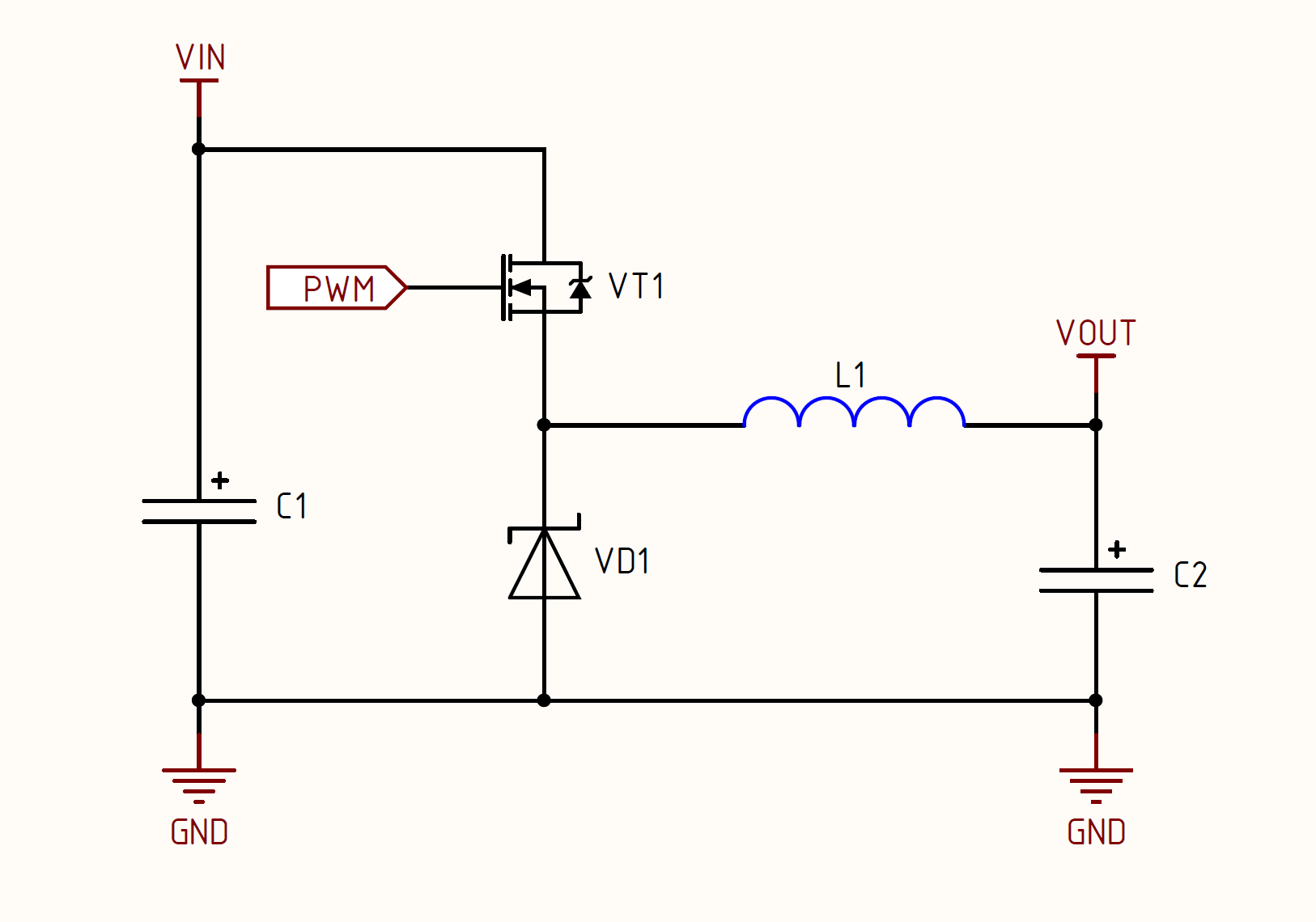
I will begin to tell from the very basics and will gradually improve our converter, since “Synchronous buck” is an improved version with increased efficiency and control complexity. The basic topology, which you probably used, is as follows:
This topology is used in low-power voltage converters, for example, to power digital circuits and other low-power devices. The dc / dc downgrades that you use in your devices are most likely implemented on microchips for this topology. An example of such a chip LMR16006 .
The principle of operation of this circuit is very simple, the PWM signal is sent to the VT1 transistor, the work itself is divided into 2 stages, which alternate one after another:
- Stage of energy storage in the LC circuit. At this stage, the transistor VT1 is open and the current flows through the transistor to the load, simultaneously accumulating energy in the inductance coil and output capacitance:

- Stage of discharge. At this stage, the transistor VT1 closes and the most interesting begins. A choke is such a thing that accumulates energy if a potential is applied to it (open VT1) and gives it away if the potential disappears (VT1 is closed). At the same time, he seeks not only to give energy, but to preserve the current value and its direction, therefore, in order to use this property, you need to add a VD1 diode to close the circuit, because the current flows only in a closed circuit:

When I got acquainted with this topology at 6-7m class, I didn’t understand right away why the diode does not conduct current at the 1st stage, now it seems trivial, but I think it is worth mentioning. When VT1 is open, a + VIN potential is applied to the cathode of the VD1 diode, for example, + 20V, and a ground potential is applied to the diode anode. In order for the current to flow through the diode it should be exactly the opposite: the potential at the anode must be greater than the potential at the cathode, therefore, in a buck, the diode is “closed” at the energy accumulation stage. At the stage of discharge, the diode already closes the circuit, the potential + VIN does not act on its cathode and does not “lock” it. I hope clearly explained.
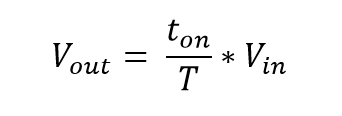
Here you should have a question: “And what voltage will be at the output, if we applied to the input 20V?”. As always, everything is simple:
As can be seen from the formula, the output voltage linearly depends on the duty cycle (duty) of the PWM signal, which we apply to the VT1 transistor. If someone does not know or has forgotten the “duty ratio” is the ratio of the time that the transistor is in the open state to the period duration. This ratio can take a value from 0 to 1 or from 0 to 100%. Then we will operate with this particular figure when controlling the converter, but for understanding the essence let's substitute this relation into the formula:
The frequency of the buck-converter value is constant and is selected when designing, during operation it does not change, and therefore the period (T) is constant. It turns out that the output voltage directly depends on two physical quantities:
- from the time at which we open the upper transistor (VT1) - the longer it is open, the more energy accumulates in the LC filter and, accordingly, the higher the output voltage;
- from the input voltage, for example, if we fixed the filling to 50% and change the Vin from 20 to 40V, then the output voltage will also vary from 10 to 20V.
I think you have started to see the overall picture and the principle of work, let's fix it now and look at the real oscillograms and check this ratio in practice. I have assembled a buck model, which is loaded with a 10W LED. I used 3 oscilloscope channels, which are included in the following points:
Test №1 - Input voltage (Vin) constant 20V, changing the fill factor
- Vin = 20V, D = 25%, Vout = D * Vin = 0.25 * 20V = 5V

- Vin = 20V, D = 50%, Vout = D * Vin = 0.5 * 20V = 10V
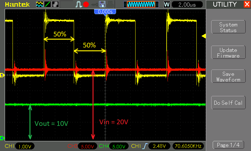
As you can see on the oscillograms, the relation between the output voltage and the fill factor is correct. Of course, this was an “idealized” experiment; in reality, the input voltage is not stable and floats in a fairly wide range. Let's now see what will be the dependence on the input voltage with a fixed filling.
Test No 2 - The input voltage (Vin) changes, the fill factor is constant and is 50%.
- Vin = 15V, D = 50%, Vout = D * Vin = 0.5 * 15V = 7.5V
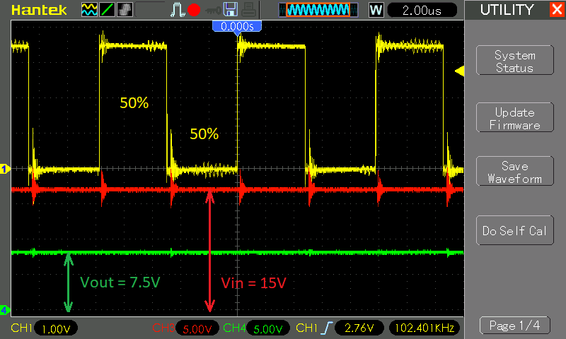
- Vin = 20V, D = 50%, Vout = D * Vin = 0.5 * 20V = 10V

- Vin = 30V, D = 50%, Vout = D * Vin = 0.5 * 30V = 15V

Now we are convinced in practice that the output voltage also linearly depends on the input voltage with a fixed fill factor. Understand how to stabilize the output? The principle of stabilization is simple as the formula itself - Vout is 12V and a constant, we can change the fill factor using a microcontroller, so if Vin increases, then the output voltage increases and at this point we decrease the fill factor (duty) again until 12V. Accordingly, with a decrease in Vin, we begin to increase the fill factor until, again, the voltage Vout becomes 12V.
What else would you like to pay attention to in the theoretical section ... Oh, yes! Surely you wonder how PWM with an amplitude of 20V after the transistor eventually turned into a constant voltage with scanty pulsations? Indeed, if we put the red probe of the oscilloscope at the source of the transistor VT1, the green probe after the LC filter, we will see the following picture:
You can see how the LC-filter "lubricates" the alternating voltage into a constant, but the point is that the energy stored in the inductance and capacitance cannot be instantly consumed, hence the voltage cannot instantly change. We get that at the moment when the PWM before the choke is 0V, the output voltage is provided by the energy stored in the filter, which does not dissolve instantly and is enough to maintain the voltage at the time of closing VT1. This is all on the fingers of course, if it is interesting to go deeper, then as always I advise you to start the book B.Yu. Semenova "Power electronics: from simple to complex" , there is a whole chapter on the buck (chopper).
Fight for efficiency
As I wrote a little earlier - it was a basic version of the topology. Its main disadvantage is high losses on the blocking diode. What current in the simple systems working on MK and CPLD? Usually within 1A, sometimes 2A, if there is some TFT display. In this case, the loss even when using a Schottky diode will be 0.4V * 2A = 0.8W. In principle, it is tolerable, it is possible to dissipate so much on the SMA / SMB case without problems, although at a voltage of 3.3V and 2A a loss of 0.8V is still 12% efficiency!
Now imagine a case where the current is 20A. It could be an MPPT controller, a large FPGA power system and much more. In this case, the loss will be 0.4V * 20A = 8 W! What does it mean? For example, in the case of MPPT, you will have less energy stored in the battery, in the case of powering the FPGA it will be an additional 8 W of heat that needs to be dissipated somewhere and in both cases it is undoubtedly a loss of overall efficiency. What can be done? And let's replace the VD1 diode with another N-channel Mosfet and get the following circuit:
Now the transistor VT2 acts as a diode, that is, conducts a current when VT1 is closed. The diode, which was in the basic version did not require control, but now we have to pay for an improvement in performance with an additional control channel with a PWM signal.
First, let's calculate how much we have reduced losses. The resistance of the channel of the modern mosfet is a few mΩ. As an example, let's take a transistor from my power module, which I described in previous articles - IPP083N10N5AKSA1 with a channel resistance of 8.3 megohms. We get static losses equal to 0.0083 * 20A * 20A = 3.32 W. Of course, there will also be dynamic losses, which with an adequately designed driver will be no more than 20%, that is, the total losses will be 4W. We get that the transition from the usual buck-to synchronous allows halving the losses on the diode.
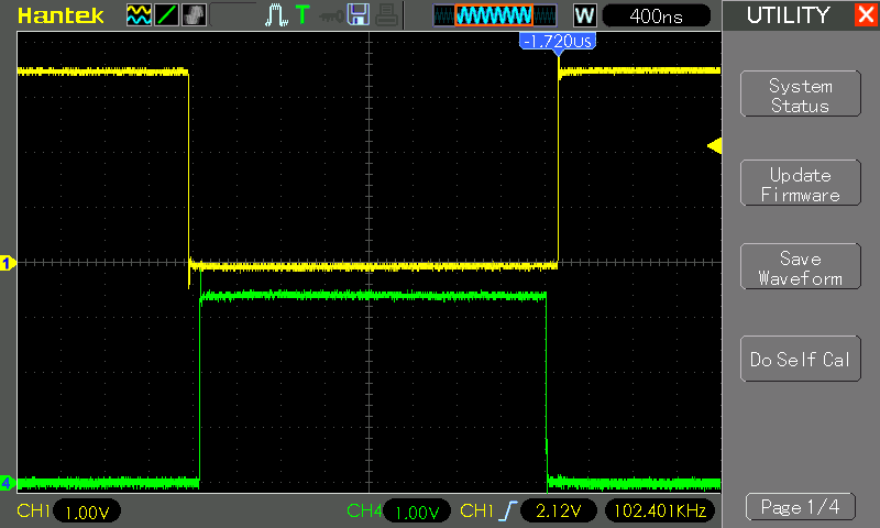
Let us now analyze the complicated management. As we already understood, the blocking diode conducted the current when VT1 was closed. From this it follows that VT2 must be closed when VT1 is open and, accordingly, VT2 is open when VT1 is closed. If it is simpler, the transistors work alternately: or one is open or the other, if both transistors open, a through current will arise, since they are closed between themselves VIN and GND. Let's see what should be the signal, where the “yellow channel” is a VT1 transistor and the “green channel” is a VT2 transistor:
As you can see, if the logical channel “1” is set in the yellow channel (on VT1), then at that time a logical “0” should be set in the green channel (on VT2). We obtain that VT1 pumps energy into the LC filter, and VT2 closes the circuit at the stage of discharge.
There is one more thing about which you have already heard or read above - through - through current . The fact is that a real, not an ideal transistor (mosfet) has a certain capacity on the gate, that is, in reality, it does not instantly go from log.0 to log.1, and the energy in the transistor does not dissolve instantly, resulting in transistors for a short time at the moment of switching may both be open. This can lead in the best case to increased losses, which means heating up and in the worst case to the woman, since Through current is a common short circuit (short circuit). To avoid this, between turning off one transistor and turning on another, a delay, or so-called dead-time, is introduced. It looks like this:
I think you noticed that there is a small space on the signal switching edge. I installed it obviously large (about 3%) so that you can see it, in reality it is much smaller. In general, dead-time (further dt) is set as short as possible, but at the same time sufficient for the transistors to close. It can be calculated, or it can be chosen empirically, I personally think that this and that option is normal, but bearded Jedi will surely tell you: “It must be considered necessary, but it is better to simulate!”. This is certainly correct, but decide for yourself - if you are not too lazy to model in LTspice taking into account the parasitic inductances and capacitances of conductors and components.
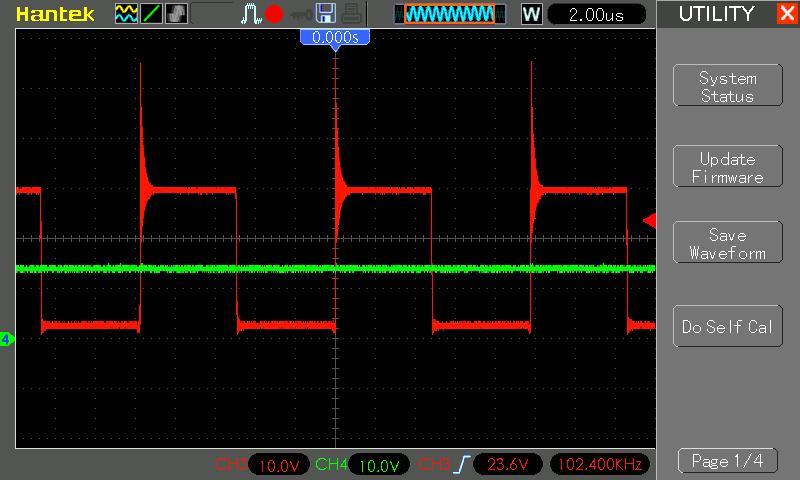
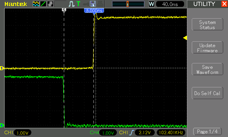
For the stand in this article, I set the dt to ~ 100 ns (actually 104). My module allows you to install it significantly less, because The driver is very harshly applied, but surely many of you will assemble your layout without my module, which means there will most likely be snot there. I’ll leave dt with a margin so that I don’t bang because of the snot, and if you have a normal layout on the board, then you can reduce it yourself - then in the chapter on the code you will see how, but in the meantime we’re actually looking at dt:
Here you can see that dt lasts 2.5 divisions and each division is 40 ns - it means that the duration is ~ 100 ns as intended. I hope you understand why dt is needed, how long it should be, and how the buck topology works in general. If you do not understand, then as usual the questions in the comments, HP and the mail are accepted, while I seem to be answering everything.
Chapter 2. The calculation of the main components
In this part of the article, I will show how to quickly and simply calculate the main power components for a synchronous buck-converter, namely: choke, input and output capacitors, transistors.
I recall the introductory data:
- Input voltage: 15 ... 30V
- Output voltage: 12V
- Rated output current: 2A
- Switching frequency: 100 kHz
Output voltage 12V is selected because As a load, I plan to use a 12V 20W LED, which is at hand and is a very visual load. Anticipating the questions of the “experts” in the comments - yes, I am aware that the LED needs current stabilization, but we do a voltage regulator and the LED is just a load.
The input voltage is chosen from the bald, you can do 15 ... 60V, so if you are interested in a different range, you can calculate the value of the components for it. A rated current of 2A is chosen to obtain an output power of 12V * 2A = 24 W, that is, slightly more than is needed for the LED. The LED itself at 12V consumes about 1.82 ... 1.9A.
The most interesting parameter remained - the operating frequency of the converter. What should it be? Here you have to answer yourself, in my case it is 100 kHz. The choice is based on two theses:
- Increasing the frequency leads to a decrease in the required inductance of the choke, the input and output capacitors. Simply put, as the frequency increases, the size of the device decreases. With decreasing frequency, dimensions increase.
- Reducing the frequency leads to an increase in efficiency, because dynamic losses when switching transistors are reduced. Increasing the frequency increases the dynamic component of the transistors and accordingly reduces the efficiency.
Now I will not talk about the choice of frequency, just accept that 100 kHz. After I show the calculation method, we will return to this question, because the formulas will more clearly show the dependence of the denominations of the main components of the operating frequency.
Step 1. Select transistors
We will be mainly interested in 3 parameters: maximum drain-source voltage, channel resistance in the open state and gate capacitance. The entire potential of the voltage source (Vin) is applied to the transistor, and there are also spikes at the moment of switching. You have 2 options: take the transistor VT1 and VT2 with a voltage margin or the story RC snubber at VT2. In my case, there are 100V transistors on the power module, and with an input 30V, this is a huge voltage margin, even 60V was enough to do without snubber and protect the transistor from breakdown.
Channel resistance - here the less, the better, but there is one BUT. With a decrease in channel resistance, we reduce static losses (I 2 * R), but the technology is such that the capacity of the shutter increases, and this leads to an increase in dynamic losses. You have to find a middle ground between the "channel resistance" and "gate capacity". For voltages up to 100V, I advise you to pay attention to Infineon's OptiMOS series transistors; you can already look at high voltages for parametric search or even towards IGBT transistors. The latter are also supported by my power module and do not require any changes in the driver.
Step 2. Calculate the inductor inductance
It is necessary to calculate the minimum value of inductance, which will allow our dc / dc converter to work in the continuous current mode (L min ):
For variables, I think everything is clear, except - k ind . These are permissible ripple currents in the choke, usually choose the value of 20 ... 50%, but I almost always set 30%. The smaller the ripple of current, the further we will be from the saturation limit of the core on which the choke is wound, but as can be seen from the formula, we need a large inductance of the choke.
Now we calculate the minimum value of inductance, which is needed for my input data, ripple, I will lay 30% as already written above:
It should be understood that this is the minimum inductance required for the buck-converter to operate in the continuous current mode, but again there is a nuance. In the process of increasing the current acting in the winding, the permeability of the core and the inductance of the choke WITHOUT current and With the current are slightly different, somewhat different for different materials. In order to avoid the situation when the inductance decreased below L min and the dc / dc did not go into the discontinuous current mode when the current increased in the inductor, it is necessary to slightly increase the inductance, that is, add a couple of extra turns during the winding. Increasing the inductance by 10-15% will be enough for the material Kool Mu, and my choke will be on it.
Step 3. Calculation and manufacture of the throttle
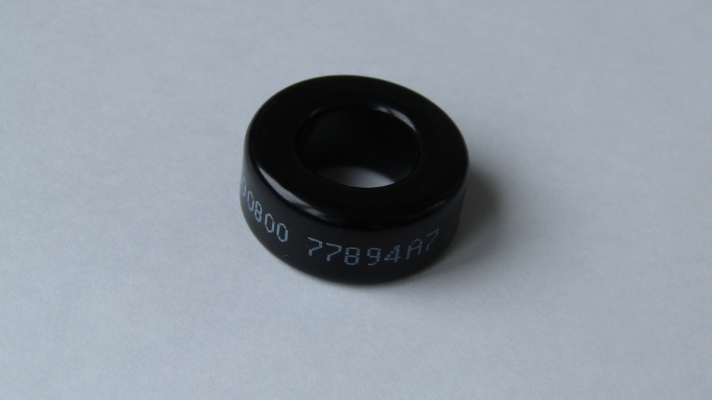
I wanted to describe this procedure in the “prototyping” section, but then the inductance calculation stage would have remained less clear for you, and probably missed the interesting pictures, so I’ll describe everything here. For the manufacture of the throttle, I will take the throttle R26 / 14/11 (R is a ring, and the numbers are dimensions) from the material Kool Mu with permeability 60, download the documentation on it and you can buy it here - Lepkos .
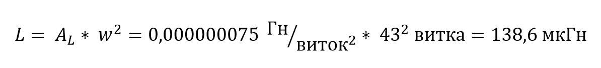
Now you need to count how many turns and which wire to wind. Let's start with the number of turns perhaps. In the documentation on the core there is such a convenient parameter - A L , which is equal to 75 nH / revolution 2 . Here carefully - the turns in the square! To find the inductance of the core, you must multiply A L by the number of turns in the square. Hence, the formula for finding the number of turns looks like this:
In order to obtain the minimum required inductance, it is necessary to wind 40 turns, but as we have already discussed, it is necessary to slightly increase the inductance, say, throw +3 turns. Take the ring and wind 43 turns, we get the following choke:
Now for the sake of interest let's calculate what inductance should be:
And for reliability, we check the inductance of the choke with tweezers:
137 μH, great! The results agreed, the error is within ± 8% for A L. Here it is worth noting - if you do not have the ability to measure inductance, then do not buy cores for aliexpress, in ChiD, complex, electronic engineer and other “eatery” - there is a chance to get a core from another material or not that permeability, but with proper marking - verified. Without the ability to measure inductance, you will not be able to test A L and you will be able to spend a lot of time searching for the cause of the “broadshaft” of your converter.
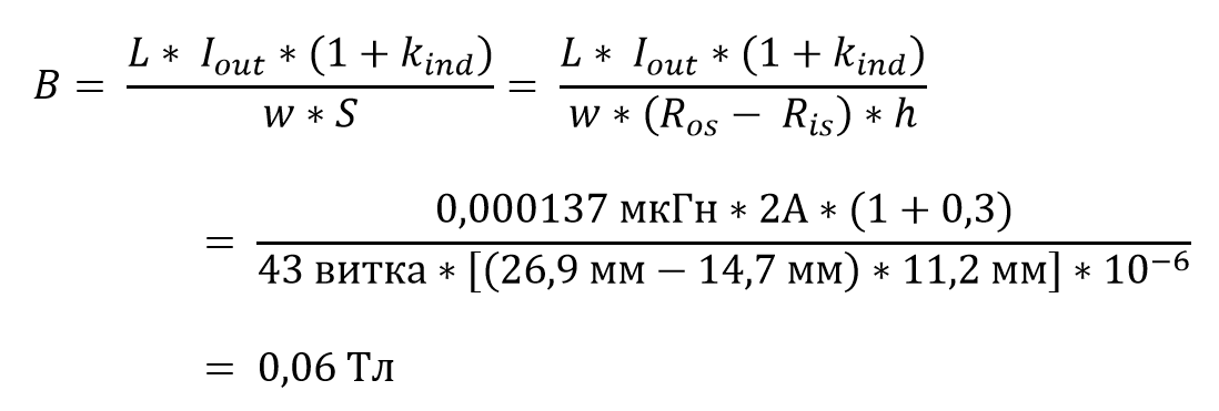
Then a reasonable question will appear - “will we have enough of the core and its dimensions? Maybe it was necessary more? ". For the material Kool Mu, the magnetic induction limit is 0.5 T, in practice it is better not to climb over the threshold above 0.45 T without obvious need. It turns out that the winding wound on the core does not have to create an induction at each point of the core more than 0.45 T, so check:
As you can see, the value of magnetic induction 0.06 T is much lower than the limit 0.5 T. Two conclusions can be drawn from this: firstly, the throttle will not go into saturation, and secondly, the core is very large and powerfully take a ring of substantially smaller size. I took the ring R26 simply because I have a whole box of them, there is no other secret meaning here.
It remains to determine what wire size to take for the choke. Firstly, I strongly advise you not to take a wire with a diameter of more than 1 ... 1.2 mm at such high frequencies, since The skin effect already has a significant effect and reduces the effective cross section. Secondly, the current density in the wire must be selected based on the conditions of cooling and power. At low powers (up to 10–20 W), it is possible to safely lay a current density of 8. 10 A / mm 2 even without airflow. At powers up to several kilowatts, it is better to lay the current density in the range of 5 ... 6 A / mm 2 , and at powers from 10 kW and further it will be reasonable to reduce the current density to 3 ... 4 A / mm 2 .
I had a varnished wire with a diameter of 0.8 mm on hand. Its cross section, respectively, is ~ 0.5 mm 2 . At a current of 2A, we obtain a current density in the winding of about 4 A / mm 2 . I could use a wire and half the size of the cross section, but my core is large enough, so the wire of a larger cross section got in without problems. When you optimize your device, you will have to first read and then buy the wire of the desired cross section, then you will be able to get the optimal dimensions of the choke.
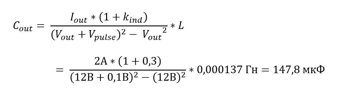
Step 4. Calculate the output capacitor
At this stage, as in the case of inductance, we will consider the minimum value of the capacitance, which must be installed in the LC filter at the output of the buck converter. Accordingly, if you install more, it will be better and then you will see why. Calculate capacity:
Of course, the capacity must also be set with a certain margin, especially if you use only ceramics at the outlet, since its capacity is greatly reduced depending on the voltage applied to it. You should also pay attention to the dependence on pulsations - the variable V pulse . This is the maximum value of the ripple at the output, that is, ideally with a capacity of 147.8 microfarads, the amplitude of the ripple will be 0.2 V, that is, the output voltage will float in the range of 11.9 ... 12.1 V. Want to reduce ripple? Then reduce them in the formula and the value of the resulting capacity will increase accordingly, of course, you will not get a laboratory power supply simply by increasing the output capacity. It is also necessary to take into account the need for a low ESR, for this purpose, 1-2 electrolytes are usually put in parallel and in parallel they are hung with ceramics a few microfarads with the X7R dielectric desirable. If the budget allows, then you can replace the electrolytic capacitor with polymer tantalum (as in a GPU) and so ceramics are not needed, they have an ESR and so little.
Frequency considerations
Now, as I said, let us return to the question of choosing the operating frequency of the converter. Let me divide the conclusions into several thoughts:
- , , —
- , , 2 4 . , , ,
- , — , , . !
- Now for the bad ... The frequency increases, which means that the dynamic losses of transistors increase and this obviously leads to a decrease in the overall efficiency. For any significant power, a reasonable frequency limit for a buck converter on mosfet s is 200 kHz and lower. Want more power (hundreds of watts) and a huge frequency? Welcome to the world of GaN transistors or resonant topologies
I think from these theses it became clear to you what the switching frequency affects, now you need to independently learn how to find the "middle ground" between losses on transistors and the size of the device. In one of the following articles I will teach you how to optimize the working frequency for maximum efficiency, the main thing is not to forget that I was going to do it.
Chapter 3. We collect the layout of the buck-converter
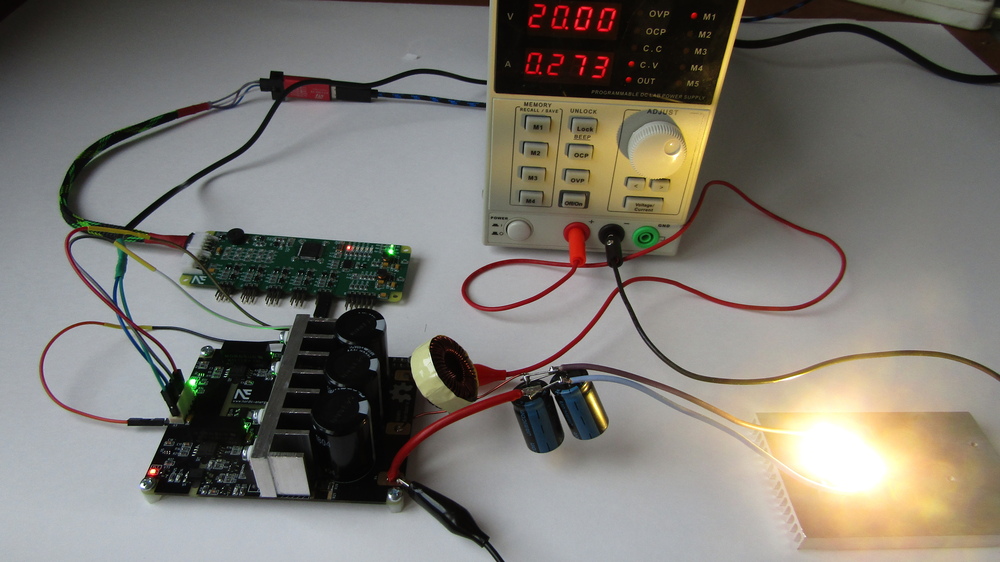
So, the most tedious, but important, part is over, now the hardware and code will go. Let's put together a model on which we will implement theoretical calculations. To do this, we need two modules about which I described in previous articles: the power module and the control module on the STM32F334 . You can also collect a half-bridge from any IR2110 waste trap yourself on the breadboard, and use any MC: STM32-Discovery, LaunchPad, Arduino and simply adapt the operation logic and code to your favorite MC; nothing will be difficult if You understood from the first two chapters how the buck converter works.
Now, let's make our structural diagram of the buck more “realistic” by adding the nominal values of all the components to it and correctly reflect the number of capacitors, as well as what part my power module can implement:
As can be seen from the diagram, the module already contains a half bridge (two transistors) for the implementation of a synchronous buck and input capacitor. By the way, the module has a huge margin in the module - there are 3 electrolytes of 1000 µF each and 100V, which is enough to build a buck for 500 -800 watts. It remains for us to add a choke, which we have already manufactured and output capacitors, the latter, too, by the way, with a margin, since I found only 4700 microfarads of 25V for low voltage, but they are some kind of Chinese, so I also decided to pair a couple. In fact, 470 uF of one is enough, but I simply didn’t have such little things in the hatchet. It turns out this design:
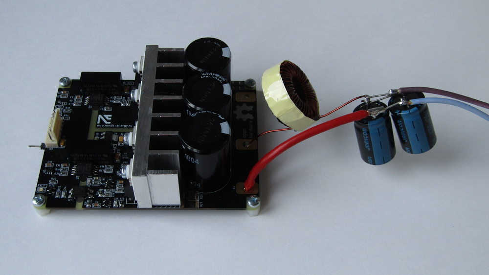
As previously mentioned, a high power 20W LED is used as a load. I don’t know how much he is shining, and it’s not very interesting, but at 12V it consumes just 21 ... 22 W, which is what my buck converter is designed for. The LED itself smeared KPT-8 and screwed it to the radiator, it is of course not enough, but it lasts 5-7 minutes of operation without problems (heats up to +40 ... 50 o C), and I don’t need more. We connect from the control module 2 signals HRPWM, GND and through the divider we catch the output of the buck to the ADC, as a result we have the following stand:
Chapter 4. We write software and run the converter
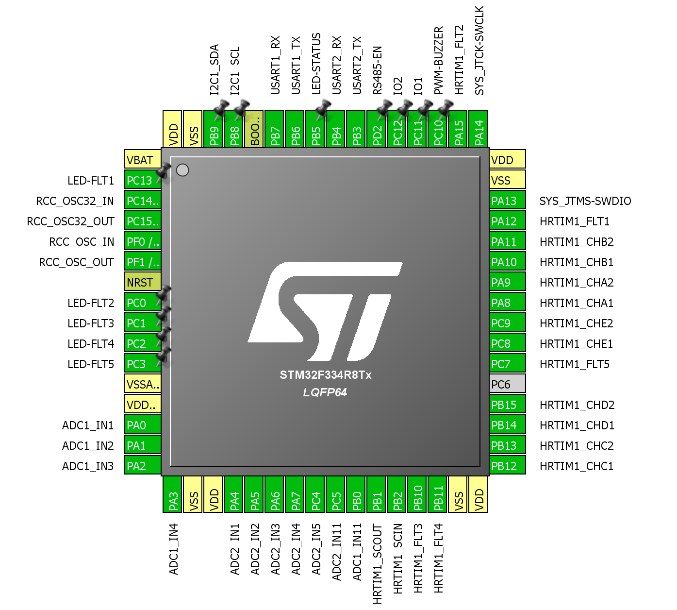
Now we have everything we need to start writing code and liven up our buck converter. First, let's look at the pin-out for the STM32F334R8T6 microcontroller, which stands in the control module:
Now we understand what the microcontroller pins will be used. On the module itself, I will need only 1 of 5 channels to control the power section; we will use channel “A”. This channel, like the others, has 2 high-precision PWM outputs (HRPWM), 1 error input (we don’t use it), GND for combining the ground of the boards and 2 ADC channels (we’ll use only one for voltage).
A little bit about HRPWM
In the open spaces of the Russian-speaking segment of the Internet, I practically did not encounter any training materials on HRPWM and did not meet at all materials on working with HRPWM based on STM32 microcontrollers, and this is a very useful peripheral.
In this article I will not delve into the theory of this periphery, so I will describe the essence. HRPWM or High Resolution PWM is a PWM module that is familiar to us, which has a higher resolution setting of the duty ratio and, in addition, usually has more flexible settings.
- The microcontroller STM32F334R8T6 has 10 HRPWM channels, which are combined into 5 groups of 2 channels each. These 2 channels within the group can work both independently and form a complementary pair - the last one we need;
- 2- dead-time ;
- 10 — Master timer, . Timer A...E ;
- HRPWM , 72 HRPWM 144 (2) PLL. ;
- , , , 4 (comp), 0 1 / ;
- There are modes for specific topologies, for example, the push-pull mode, which allows you to implement multiple push-pull topologies.
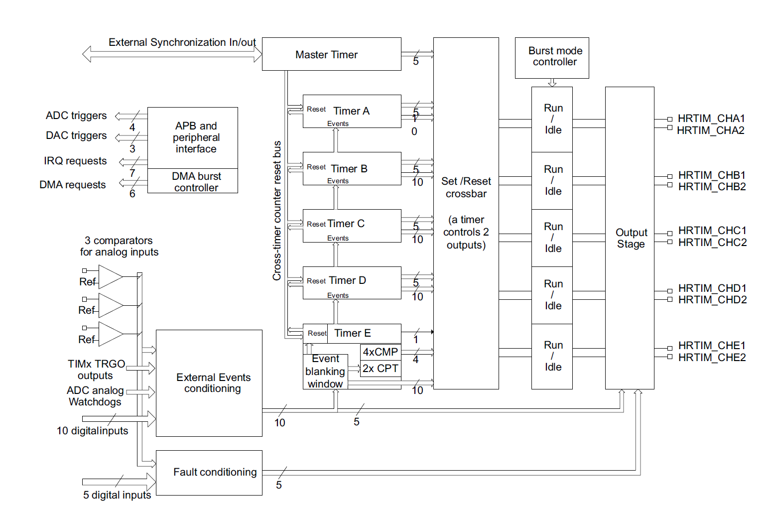
And this is only a small part of the features, on the HRPWM device diagram you can still see the possibility of synchronization with a bunch of events, DACs, built-in comparators to the MC, and alongside this flowchart there are many more documented features.
There remains the last question that needs to be addressed - “why is this PWM high-bit?”. To do this, consider a simple example. Imagine that you decided to use the MK without HRPWM, say STM32F103C8T6, which also operates at 72 MHz. We need to control a half bridge at a frequency of 70 kHz, which step of regulation we can get: 72,000,000 / 1025 steps = 70,243 Hz. Yeah, we have 1025 steps and when adjusting we can change the output voltage with a theoretical step of 1/1025 = ~ 0.1%. Now we take STM32F334, with a clocking frequency of 144 MHz and a timer shift depth of 32 bits, we get the equivalent frequency of 144 MHz * 32 = 4.608 GHz. For those who are frightened and questioned in the figure:
No, this is not the operating frequency, this is the equivalent frequency. What does this give us? We take the equivalent frequency of 4,608,000,000 Hz / 70,300 Hz = 65,535 steps. Now we can adjust the voltage (or current) at the output in 1/65 535 increments = ~ 0.001%, that is, 100 times more accurate!
And now let's do it - the frequency is 700 kHz, which is normal for a multi-phase buck, for example. F103 will have 72 000 000 Hz / 700 000 Hz = 102 steps, which allows at best to get a regulation of 1%, but this is 1% for duty, that is, in reality, with so many steps you will have voltage to float at the output as if stabilizing and no special. Whereas for F334 the number of steps will be approximately 6500, which still allows you to build a very accurate voltage or current regulator. We get that the resolution (step) of the setting of the duty ratio is much higher / more often than that of a conventional MK with a standard PWM module inside.
Setting up the clocking system
As a development environment in this article, I used TrueSTUDIO, because it is free, not as poor as Keil or IAR
After the project has been created and the LED has flashed, it is necessary to adjust the clocking system, namely from 8 MHz, raise the frequency to 72 MHz and feed it to the core, and then adjust the divider to reduce the frequency applied to the ADC:
void StartInitClock (void) { RCC->CR |= RCC_CR_HSEON; // Enable HSE while (!(RCC->CR & RCC_CR_HSERDY)); FLASH->ACR |= FLASH_ACR_LATENCY_1; RCC->CFGR |= RCC_CFGR_PLLMUL9; // PLL mult x9 RCC->CFGR |= RCC_CFGR_PLLSRC; // Source HSE RCC->CFGR2 |= RCC_CFGR2_ADCPRE12_DIV10; // ADC source AHB/10 RCC->CR |= RCC_CR_PLLON; while((RCC->CR & RCC_CR_PLLRDY) == 0){} RCC->CFGR &= ~RCC_CFGR_SW; RCC->CFGR |= RCC_CFGR_SW_PLL; // Select source SYSCLK = PLL while((RCC->CFGR & RCC_CFGR_SWS) != RCC_CFGR_SWS_1) {} // Wait PLL } Everything is simple, I think, the setup algorithm is as follows: goes to external quartz (HSE) -> wait for the transition to complete and set the ready flag -> send the PLL signal from the quartz to the input -> multiply 8 MHz by 9 -> 72 MHz, divide by 10 to clock the ADC -> turn on the PLL -> wait until it turns on and sets the ready flag -> feed the system bus and the core with the PLL -> wait until the switch is completed -> ready.
HRPWM Setup
Here everything is somewhat more complicated. There is a lot of functionality for this module, a lot of configurations and the amount of documentation is very large, but this is a minus and at the same time a plus - you have to pay for flexibility.
RCC->CFGR3 |= RCC_CFGR3_HRTIM1SW_PLL; RCC->APB2ENR |= RCC_APB2ENR_HRTIM1EN; It is necessary to indicate that HRTIM is clocked from the PLL, the multiplier x2 is already on by default. Then we just turn on clocking for HRTIM, here is the first feature - as we understand the timer is clocked by PLL, but turned on for APB2. This is not entirely logical, but in a file with CMSIS it is easy to search or in the documentation.
RCC->AHBENR |= RCC_AHBENR_GPIOAEN; GPIOA->MODER &= ~GPIO_MODER_MODER8; GPIOA->MODER |= GPIO_MODER_MODER8_1; // Alternative PP GPIOA->OSPEEDR |= GPIO_OSPEEDER_OSPEEDR8; // Very high speed GPIOA->MODER &= ~GPIO_MODER_MODER9; GPIOA->MODER |= GPIO_MODER_MODER9_1; GPIOA->OSPEEDR |= GPIO_OSPEEDER_OSPEEDR9; GPIOA->AFR[1] |= 0xDD; // PA8 and PA9 - AF13 PA8 and PA9 is the output of Timer A, which on my module goes to channel No. 1, which you can see on the diagram and pin-out. The legs are configured as a push-pull with an alternative function, the number of the function for both legs is the 13th. It is also important to tune to the maximum GPIO frequency, otherwise it will be an incomprehensible blockage of the front and the fall of the signal, which is extremely critical for power electronics.
HRTIM1->sCommonRegs.DLLCR |= HRTIM_DLLCR_CAL | HRTIM_DLLCR_CALEN; while ((HRTIM1->sCommonRegs.ISR & HRTIM_ISR_DLLRDY) == RESET); Before you start, you need to calibrate the timer, because it works with minimal delays, then just wait for the ready flag.
HRTIM1->sTimerxRegs[0].PERxR = PeriodTimerA; // Period for timer A HRTIM1->sTimerxRegs[0].CMP1xR = 0; // Duty for timer A That went flexibility. Firstly, we can set our own frequency for each timer A ... E, then we simply record the period of our PWM. Secondly, by default we have the PIMA alignment at the beginning of the period, that is, the signal goes to log.1 at the beginning of the new period, and now we need to choose when it returns to log.0, in this case by comparator No. 1, that is I ask in it the essence of the fill factor (duty).
For example, you can translate PWM not at the beginning of the period, but by comparator # 1, but return to log.0 by comparator # 2 and thus move the phase by hardware.
// Deadtime enable HRTIM1->sTimerxRegs[0].OUTxR |= HRTIM_OUTR_DTEN; // Tdtg = 6.94 ns HRTIM1->sTimerxRegs[0].DTxR |= HRTIM_DTR_DTPRSC_0 | HRTIM_DTR_DTPRSC_1; // Deadtime rising = 15*Ttg = 104 ns HRTIM1->sTimerxRegs[0].DTxR |= HRTIM_DTR_DTR_0 | HRTIM_DTR_DTR_1 | HRTIM_DTR_DTR_2 | HRTIM_DTR_DTR_3; // Deadtime falling = 15*Ttg = 104 ns HRTIM1->sTimerxRegs[0].DTxR |= HRTIM_DTR_DTF_0 | HRTIM_DTR_DTF_1 | HRTIM_DTR_DTF_2 | HRTIM_DTR_DTF_3; HRTIM1->sTimerxRegs[0].DTxR |= HRTIM_DTR_DTFSLK | HRTIM_DTR_DTRSLK; At this stage, we include the dead-time and set it up, in principle there are all the formulas in the comments, they can also be found in the reference manual. DT with a duration of ~ 100 ns you have already seen on the oscillogram in the theoretical chapter of this article. Dead time can be set separately on the front and on the decline of the signal. By the way, [0] is Timer A, respectively [1] is Timer B and so on.
// Samples in middle of ON time HRTIM1->sTimerxRegs[0].CMP2xR = PeriodTimerA / 10; // ADC trigger 1 update: Timer A HRTIM1->sCommonRegs.CR1 |= HRTIM_CR1_ADC1USRC_0; // ADC trigger 1 event: Timer A compare 2 HRTIM1->sCommonRegs.ADC1R |= HRTIM_ADC1R_AD1TAC2; For me it was not the most obvious point. Essentially, I want to make it so that at 10% of the duration of the Timer A period, an event is generated that would trigger the ADC conversion and measure the feedback signal. Why 10%? Just ideally, the measurement should not occur at the time of the transition of PIM from 0 to 1 or vice versa, because at this moment transients and disturbances occur in the power section, and we do not need to measure them. Therefore, in my case, 10% is optimal, since at 12V output and 30V input voltage of the duty cycle (duty) does not fall to 10% and the switching time of the transistor does not exactly coincide with the measurement of the ADC.
Now we need to look at the event communication system between HRTIM and the ADC:
In the first line, we choose exactly when the comparator will work, in my case it is 10% of the period of timer A. Next, we select a specific trigger in the ADC that MK will contact, 1 or 3 is available. Now it simply indicates which event will send a signal to the ADC, in my case it is comparator # 2.
// Enable output PWM for TA1 and TA2 HRTIM1->sCommonRegs.OENR |= HRTIM_OENR_TA1OEN | HRTIM_OENR_TA2OEN; // Continuous mode HRTIM1->sTimerxRegs[0].TIMxCR |= HRTIM_TIMCR_CONT; // Period for master timer HRTIM1->sMasterRegs.MPER = 65000; // Enable counter for Master and timer A HRTIM1->sMasterRegs.MCR |= HRTIM_MCR_MCEN | HRTIM_MCR_TACEN; And the final chord! We allow HRTIM to output signals from Timer A to our GPIO. Now we select the mode, it can be infinite (I have it), and it happens that the timer is turned on for 1 period and after that it must be started again. Next, set the period for the Master timer and turn it on with the last step, it starts clocking the channel timers and the PWM signal appears at the output.
It was a setup function, it remains to make a function that will set the fill factor (duty), it is with it that we will work when creating the regulator:
void SetDutyTimerA (uint16_t duty) { HRTIM1->sTimerxRegs[0].CMP1xR = duty; } Listing the function settings and set the fill factor
// f = 102,4 kHz #define PeriodTimerA ((uint16_t)45000) void InitHRPWM (void) { RCC->CFGR3 |= RCC_CFGR3_HRTIM1SW_PLL; RCC->APB2ENR |= RCC_APB2ENR_HRTIM1EN; /************************************************ * Setting GPIO ***********************************************/ RCC->AHBENR |= RCC_AHBENR_GPIOAEN; // Alternative PP GPIOA->MODER &= ~GPIO_MODER_MODER8; GPIOA->MODER |= GPIO_MODER_MODER8_1; // Very high speed GPIOA->OSPEEDR |= GPIO_OSPEEDER_OSPEEDR8; GPIOA->MODER &= ~GPIO_MODER_MODER9; GPIOA->MODER |= GPIO_MODER_MODER9_1; GPIOA->OSPEEDR |= GPIO_OSPEEDER_OSPEEDR9; // PA8 and PA9 - AF13 GPIOA->AFR[1] |= 0xDD; /************************************************ * Setting timer A ***********************************************/ HRTIM1->sCommonRegs.DLLCR |= HRTIM_DLLCR_CAL | HRTIM_DLLCR_CALEN; while ((HRTIM1->sCommonRegs.ISR & HRTIM_ISR_DLLRDY) == RESET); // Period for timer A HRTIM1->sTimerxRegs[0].PERxR = PeriodTimerA; // Duty for timer A HRTIM1->sTimerxRegs[0].CMP1xR = 0; // Deadtime enable HRTIM1->sTimerxRegs[0].OUTxR |= HRTIM_OUTR_DTEN; // Tdtg = 6.94 ns HRTIM1->sTimerxRegs[0].DTxR |= HRTIM_DTR_DTPRSC_0 | HRTIM_DTR_DTPRSC_1; // Deadtime rising = 15*Ttg = 104 ns HRTIM1->sTimerxRegs[0].DTxR |= HRTIM_DTR_DTR_0 | HRTIM_DTR_DTR_1 | HRTIM_DTR_DTR_2 | HRTIM_DTR_DTR_3; // Deadtime falling = 15*Ttg = 104 ns HRTIM1->sTimerxRegs[0].DTxR |= HRTIM_DTR_DTF_0 | HRTIM_DTR_DTF_1 | HRTIM_DTR_DTF_2 | HRTIM_DTR_DTF_3; HRTIM1->sTimerxRegs[0].DTxR |= HRTIM_DTR_DTFSLK | HRTIM_DTR_DTRSLK; // Event forces the output to active state for TA1 HRTIM1->sTimerxRegs[0].SETx1R |= HRTIM_SET1R_PER; // Event forces the output to inactive state for TA1 HRTIM1->sTimerxRegs[0].RSTx1R |= HRTIM_RST1R_CMP1; /************************************************ * ADC trigger intialization (with CMP2 event) ************************************************/ // Samples in middle of ON time HRTIM1->sTimerxRegs[0].CMP2xR = PeriodTimerA / 10; // ADC trigger 1 update: Timer A HRTIM1->sCommonRegs.CR1 |= HRTIM_CR1_ADC1USRC_0; // ADC trigger 1 event: Timer A compare 2 HRTIM1->sCommonRegs.ADC1R |= HRTIM_ADC1R_AD1TAC2; /************************************************ * HRTIM start ***********************************************/ // Enable output PWM for TA1 and TA2 HRTIM1->sCommonRegs.OENR |= HRTIM_OENR_TA1OEN | HRTIM_OENR_TA2OEN; // Continuous mode HRTIM1->sTimerxRegs[0].TIMxCR |= HRTIM_TIMCR_CONT; // Period for master timer HRTIM1->sMasterRegs.MPER = 65000; // Enable counter for Master and timer A HRTIM1->sMasterRegs.MCR |= HRTIM_MCR_MCEN | HRTIM_MCR_TACEN; } void SetDutyTimerA (uint16_t duty) { HRTIM1->sTimerxRegs[0].CMP1xR = duty; } Now let's find out if we are going the right way. In the main function, we initialize the HRTIM setting and set the duty cycle, say 22500. With an input voltage of 20V and a period of 45000, our fill factor will be 50% and the output will be about 10V. This is not enough to blow up the LED to the full, but it should catch fire and we will understand if the power part is working, is everything good with dt and so on. I started everything from the first time:
You can see that all previous theoretical calculations have been confirmed. With a fixed duty cycle (duty) of 50%, the output voltage was simply divided into 2: 20V -> 10V, 22V -> 11V, 18V -> 9V. Now let's make it so that the voltage at the output is stable and does not depend on the input, that is, we add feedback.
Setting ADC and regulator
About ADC in STM32 a lot has already been written to me, I elaborated on only setting up a trigger tied to the HRTIM comparator. I will briefly tell you about the rest of the ADC settings. We look at the initialization function:
void InitBasicADC (void) { RCC->AHBENR |= RCC_AHBENR_ADC12EN; RCC->AHBENR |= RCC_AHBENR_GPIOCEN; /************************************************ * Calibration ***********************************************/ ADC2->CR &= ~ADC_CR_ADVREGEN; ADC2->CR |= ADC_CR_ADVREGEN_0; // Vref enable Delay(10); ADC2->CR &= ~ADC_CR_ADCALDIF; ADC2->CR |= ADC_CR_ADCAL; // Start calibration while (ADC2->CR & ADC_CR_ADCAL); // Wait end calibration /************************************************ * Select event trigger and channel ***********************************************/ // Enable start conversion external trigger ADC2->CFGR |= ADC_CFGR_EXTEN_0; // Event 7 - HRTIM ADC2->CFGR |= ADC_CFGR_EXTSEL_0 | ADC_CFGR_EXTSEL_1 | ADC_CFGR_EXTSEL_2; // Select ADC2 channel IN5 ADC2->SQR1 |= ADC_SQR1_SQ1_0 | ADC_SQR1_SQ1_2; // Length regular ADC channel = 1 ADC2->SQR1 &= ~ADC_SQR1_L; ADC2->IER |= ADC_IER_EOCIE; // Interrupt enable NVIC_EnableIRQ(ADC1_2_IRQn); // enable interrupt ADC1 and ADC2 /************************************************ * Start ADC ***********************************************/ ADC2->CR |= ADC_CR_ADEN; // Enable ADC2 Delay(10); ADC2->CR |= ADC_CR_ADSTART; } I use the regular channel mode, I have only one channel and it is selected in the SQR1 register. Enabled the ADC number 2, namely, its input IN5, it is fast and can operate at the maximum sampling frequency, but not this time. The sampling rate is equal to the PWM frequency, since 1 period = 1 sample, in principle, this is more than enough.
We also need to select an event in the CFGR register that will trigger the conversion, that is, Event 7 , why exactly? Look in RM:
Trigger 1 from the HRPWM module comes to Event 7 for our ADC No. 2, which in this case works as a slave, it is controlled from the HRPWM module. I think now it is clear how to connect 2 modules, in principle, the algorithm is similar for any periphery and any timer, except the register name will be different.
Upon reaching the period counter, the master timer will start the conversion, which after about 15 cycles (how many exactly look at RM-e) will cause an interrupt and you can pick up the result. It is in this interruption that we organize the control algorithm. Yes, it’s better not to do something massively inside the interrupt, it’s better to set the flag and transfer the execution further, but I allow myself this simplification, because in this case my controller is not particularly loaded and it will be able to calculate and exit the interrupt with 146% probability the appearance of a new one.
Little about management
Imagine that you entered the bathroom and decided to wash your hands in the sink. You slightly open the water, touch with your hand, cold? Add more hot water, warmer? Good! Add more hot water? Almost what you want? Good! Add more hot water, try with your hand, burn it? Come on now, let’s cool down a little. Good? And so indefinitely you will turn the tap until the water temperature is perfect. This is the easiest regulator!
Only in our country it is not the amount of hot water that is regulated, but the fill factor of PIM. Instead of a hand, we have an ADC with measured result. It remains only to implement the logic. We will calculate that we must issue an ADC at 12V at the output, and then using the if condition, we force our controller to support this value by changing the fill factor (duty).
To begin with, let's hang up a voltage divider on the output in order to reduce 12V to 2-2.5V, for example, since The ADC can measure from 0 to + 3.3V, and if you apply 12V, the microcontroller will burn simply. Therefore, I will put a divider with nominal values of 10 kΩ and 2 kΩ, which will give a division factor of 6 and, accordingly, our + 12V will turn into + 2V. Our ADC will produce the result: adcResult = (V out / k) / V ref * 2 12 = (12V / 6) / 3.3 * 4095 = 2481. Now we write the code for the interrupt handler:
void ADC1_2_IRQHandler (void) { ADC2->ISR |= ADC_ISR_EOC; adcResult = ADC2->DR; if (adcResult > 2480) { dutyControl = dutyControl - 10; } else { dutyControl = dutyControl + 10; } SetDutyTimerA(dutyControl); } The first thing after getting into the interrupt handler is to reset the flag of the interrupt itself, otherwise the second time you will not get into it. Then we read the result and save it as adcResult variable. Now, knowing the voltage at the output, you need to make an adjustment to the value of the fill factor for PWM, I realized this simply through the if condition. In each PWM period, we measure, increase or decrease the fill factor and set the result for the next period. Everything is simple, fast and visible essence. We look at the result of the work:
As you can see, everything works and when the input voltage changes, the output itself remains stable at 12V. Strongly attentive can notice small needles skipping, then you just need to hang up the X7R ceramics at the output of 1-10 microfarads and they will leave, I'm just too lazy to look for it and solder it. Now the oscillogram itself, so as not to spoil the eyes:
Here you can see how the output voltage rises. The fact is that due to the control algorithm, the filling must reach values from 0 to 10,000, for example, a thousand periods are needed, or approximately 10 ms. It suits me because soft-start, if you want to shorten the rise time, then just complicate the algorithm and add +1000, not +10, and the closer you get to the specified 12V, the less regulation step you take until you reach +10 . In general, in terms of management, you can do a lot of things, so you have a field for experiments.
Another interesting point is the oscillations at the moment of shutdown, such an "accordion". The fact is that after turning off the power, my digital part continues to work from another power supply unit and it tries to keep the desired value at the output. Where does energy come from? Yes, from the input capacitor, these are those that are 1000 microfarads each, as many as 3 pieces, this is such an interesting phenomenon.
Conclusion
The article came out is not small, but you wanted everything and immediately say, let's get a finished piece of metal - you will get it. I hope you enjoy the article, tried to make it more likely not scientific, but popular science, so that the material was available to people with different levels of knowledge and experience. Perhaps in the future I will analyze similarly other topologies like boost, full bridge and others.
By the way, this article and code will serve for the new MPPT controller at 20A, which I am designing. Now I am waiting for PCBway boards , which, in fact , volunteered to sponsor my open source projects with printed circuit boards, the source code for MPPT will also be open to all my modules.
Most importantly forgot! Keep the project with the code for TrueSTDIO - RAR .
Source: https://habr.com/ru/post/432778/
All Articles