Processor Design (CPU Design) RAM Machine

Part I
Part II
Part III
Part IV
Part V
On Habré has already been published an article on the RAM-machine .
In general, an article about a RAM machine is on Wikipedia.
The RAM machine , which is mentioned in the book “Construction and Analysis of Computational Algorithms” - the authors: Aho, Hopkroft, Ulman - have a limited set of arithmetic commands, while in arithmetic commands we will only have “addition” and “subtraction”. In addition to arithmetic, I / O, indirect addressing, and branching commands are also available.
')
The difference between LIttle Man Computer 'a (which I described in the previous parts of the cycle) and the RAM machine is a mechanism that provides indirect addressing (the ability to work with a number stored in memory as an address).
In order to work with a number stored in memory, as with an address, connect to the address input of the Data Memory MUX multiplexer , sampling between the address itself (coming from the Command Memory ) and the number representing the address and stored in the Data Memory .
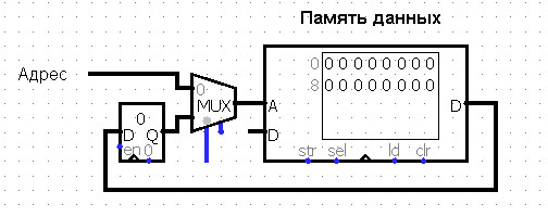
We will load the number from memory into the register each time a new command is fetched from the Command Memory . When switching the multiplexer MUX , a transition is made to the address recorded in the address register.
We will also load the load of the command address into the accumulator Acc as a number, for this we will increase the bit width of the address input of the multiplexer that selects the data to be loaded into the accumulator Ass . The address is loaded on the 4th input of the multiplexer.
The processing of the command will be done in two cycles. To do this, we connect two D-triggers to the clock generator, which will switch each other when a clock signal arrives.

The first clock cycle loads the address into the address register, the second clock cycle loads the number into the accumulator Acc or into the data memory .
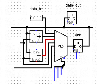
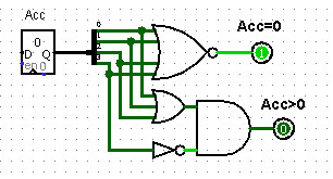
Connect to the battery 2 flags:
1. Flag Acc = 0 . The flag is raised if the contents of the ass is zero.
2. Flag Acc> 0 . The flag is raised if the contents of the ass is greater than zero.
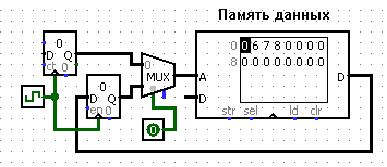
This is a scheme that can be downloaded from here.
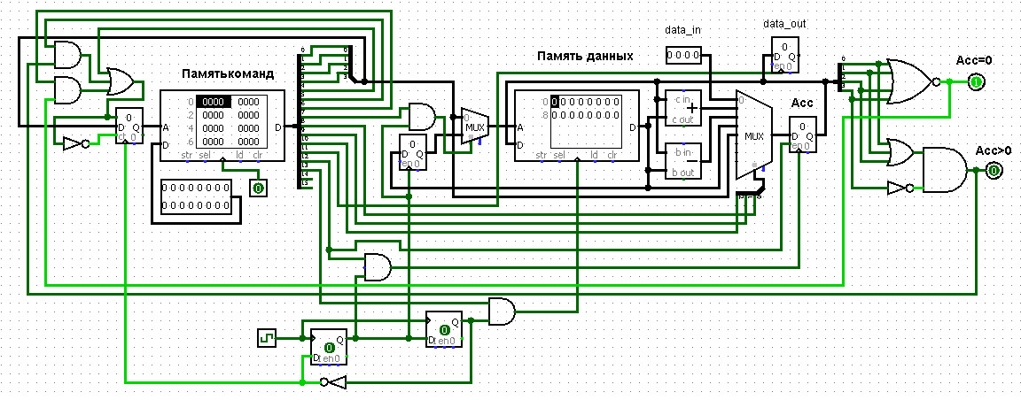
The line going to allow the input of the battery is needed to ensure that the circuit is not buggy.
Disable some commands and write a program that loads the zero cell of the data memory at the address stored in the zero cell. In the cycle, we will increase the value of the zero cell by one. So we will fill the data memory with sequence numbers.
1401 load number 1 into Acc
1100 add the number in Acc to the number in the zero cell
2000 store the result in the zero cell
2080 load a number from Acc to the address referenced by the zero cell
0010 jump to the beginning of the program

An emulator of a classic RAM machine (with separate read / write tapes) can be downloaded from here .
Check how the circuit consisting of two d-triggers works. This circuit provides a two-clock mode.
We write the scheme of the usual d-trigger (without reset and enable). It will have two input ports - a data port and a clock port.
module dff ( input [1:0] key, output led ); wire clk; assign clk = key [0]; // wire d = key [1]; // reg q; always @(posedge clk) q <= d; assign led = q; endmodule The led LED indicates the status of the d-flip-flop.
We connect two dff in the general scheme.
The status of the first d-flip-flop will be indicated by the q1_led LED.
The state of the second d-flip-flop will be indicated by the q2_led LED.
Let's output a clock signal to a separate q3_led LED.
module dff_dff ( input clk, output q1_led, q2_led,q3_led ); assign q3_led = clk; wire d1_in; assign d1_in=~q2_led; dff dff1( .clk(clk), .d(d1_in), .q(q1_led) ); wire d2; assign d2=q1_led; dff dff2( .clk(clk), .d(d2), .q(q2_led) ); endmodule RTL-model of the dff_dff module looks like
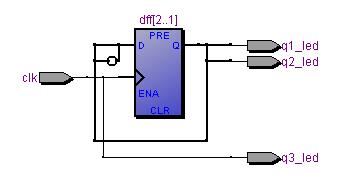
This scheme will not work on all boards, on some boards it is necessary to initialize d-flip-flops. For the same reason, such a scheme will not be simulated in ModelSim.
Source: https://habr.com/ru/post/432726/
All Articles