A tenth-grader from Siberia wants to become a processor designer. Why shouldn't she make a FPGA neuro accelerator?
Yesterday I received a letter from a tenth-grader from Siberia who wants to become a microprocessor developer. She has already received some results in this area - she added a multiplication instruction to the simplest schoolMIPS processor, synthesized it for the Intel FPGA MAX10 FPGA, determined the maximum frequency and increased performance of simple programs. She first did all this in the village of Burmistrovo, Novosibirsk Region, and then at a conference in Tomsk.
Now Dasha Krivoruchko (that is the name of the tenth grader) has moved to live in a Moscow boarding school and asks me what else to design. I think that at this stage of her career she should design a neural network hardware accelerator based on the systolic array for matrix multiplication. Use the Verilog hardware description language and Intel FPGA FPGA, but not a cheap MAX10, but something more expensive to accommodate a large systolic array.
After that, compare the performance of the hardware solution with the program running on the schoolMIPS processor, as well as with the Python program running on the desktop computer. As a test example, use the recognition of numbers from a small matrix.
')
Actually all parts of this exercise have already been developed by different people, but the whole trick is to put this into a single documented exercise, which can then be used as the basis for an online course and for practical competitions:
1) In the online course of this kind (design of a hardware at the level of register transfers + neural networks), eNano is interested, the educational department of RUSNANO, which in the past organized Charles Danchek's workshops on designing modern electronics (RTL-to-GDSII route) for students and is currently working on lightweight course for advanced students. Here we are with Charles at their office:

2) The Olympics of the NTI with whom I raised this question a couple of weeks ago in Moscow may be interested in the base for the Olympiad. To such an example, Olympiad participants could add a hardware for various activation functions. Here are colleagues from the Olympiad NTI:

So if Dasha develops this, she can theoretically introduce her well-described accelerator in both RUSNANO and the NTI Olympiad. I think it would be beneficial for the administration of her school - it would be possible to show it on TV or even send an Intel FPGA contest. Here are a couple of Russians from St. Petersburg at the finals of the Intel FPGA contest in Santa Clara, California :
Now let's talk about the technical side of the project. The idea of the systolic array accelerator is described in the article that was translated by the editor Habra Vyacheslav Golovanov SLY_G Why are TPU so well suited for deep learning?
This is the dataflow graph of a neural network for simple recognition:

A primitive computational element that performs multiplication and addition:

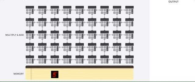
A strongly pipelined structure of such elements is a systolic array for multiplying matrices and is:
There is a bunch of Verilog and VHDL code on the Internet with the implementation of a systolic array, for example, the code under this blog post :

I will note that this code is not optimized and generally clumsy (and even unprofessionally written - the source in the post uses blocking assignments in @ (posedge clk) - I corrected it). Dasha could, for example, use Verilog generate constructions for more elegant code.
In addition to two extreme neural network implementations (on the processor and on the systolic array), Dasha could consider other options that are faster than the processor, but not as voracious in multiplication operations as a systolic array. True, this is probably not for schoolchildren, but for students.
One option is a performing device with a large number of parallel functional units, as in the Out-of-Order processor:

Another option is the so-called Coarse Grained Reconfigurable Array - a matrix of quasi-processor elements, each of which has a small program. These processor elements are ideologically similar to FPGA / FPGA cells, but operate not with individual signals, but with groups of bits / numbers on buses and registers - see Live Report from the birth of a major player in hardware AI, which accelerates TensorFlow and competes with NVidia " .
Now the original letter from Dasha:
This is how the Summer School of Young Programmers looked in the Novosibirsk region, where Dasha learned Verilog, the FPGA, the development methodology at the Register Transfer Level (RTL):


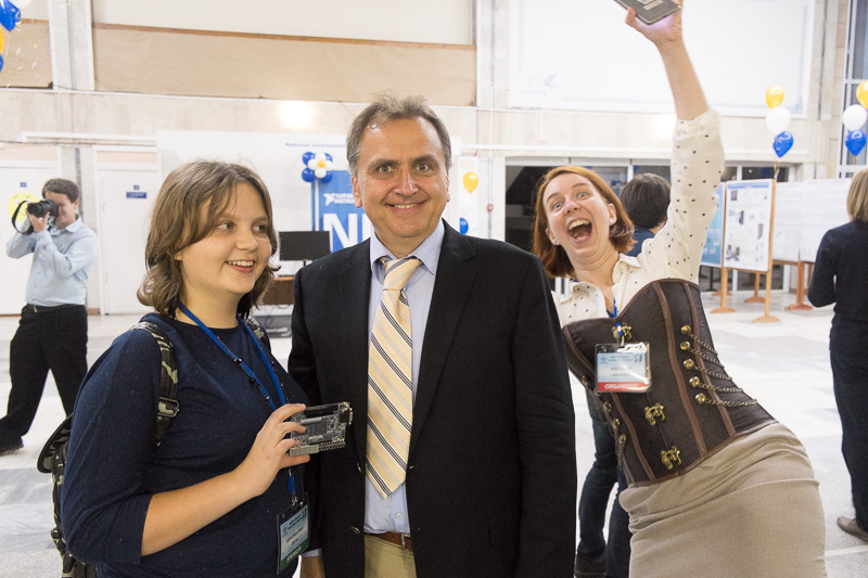
But the performance of Dasha at the conference in Tomsk, along with another tenth-grader, Arseny Chegodaev:
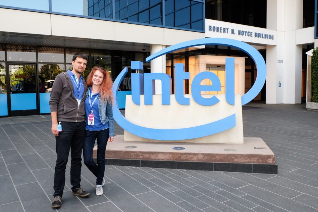
After the speech, Dasha is with me and with Stanislav Zelnio sparf , the main creator of the training processor core schoolMIPS for implementation on the FPGA:

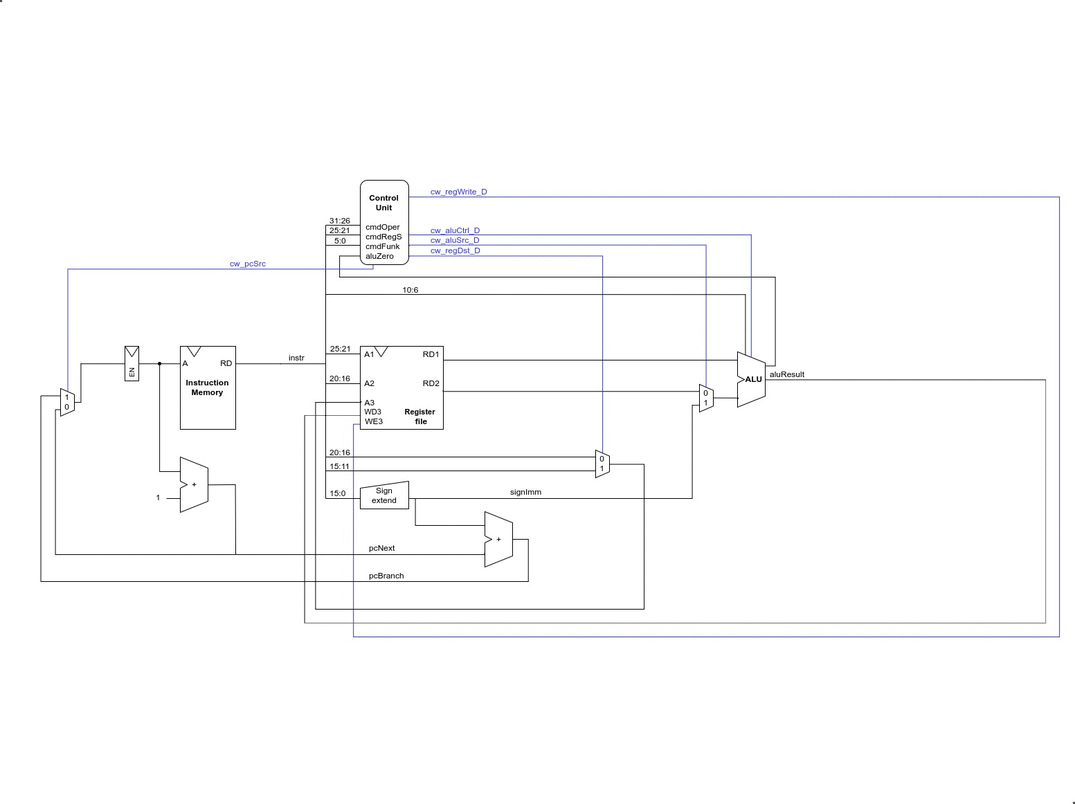
The schoolMIPS project is located at https://github.com/MIPSfpga/schoolMIPS . In the simplest configuration of this educational processor core there are only 300 lines on Verilog, while in the industrial integrated core of the middle class there are about 300 thousand lines. Nevertheless, Dasha was able to feel how the work of designers in the industry looks like, which also change the decoder and the executing device when they add a new instruction to the processor:
In conclusion, we present photos of the dean of the Samara University, Ilya Kudryavtsev, who is interested in creating a summer school and competitions with processors on the FPGA for future entrants:

And a photo of the employees of Zelenograd MIET, who are already planning such a summer school next year:

Both in one and in another place, both materials from RUSNANO and possible materials of the STI Olympiad should be well followed, as well as developments that have been made in the implementation of FPGAs and micro-architecture in the HSE MIEM, Moscow State University and Kazan Innopolis programs in the past couple of years.
Now Dasha Krivoruchko (that is the name of the tenth grader) has moved to live in a Moscow boarding school and asks me what else to design. I think that at this stage of her career she should design a neural network hardware accelerator based on the systolic array for matrix multiplication. Use the Verilog hardware description language and Intel FPGA FPGA, but not a cheap MAX10, but something more expensive to accommodate a large systolic array.
After that, compare the performance of the hardware solution with the program running on the schoolMIPS processor, as well as with the Python program running on the desktop computer. As a test example, use the recognition of numbers from a small matrix.
')
Actually all parts of this exercise have already been developed by different people, but the whole trick is to put this into a single documented exercise, which can then be used as the basis for an online course and for practical competitions:
1) In the online course of this kind (design of a hardware at the level of register transfers + neural networks), eNano is interested, the educational department of RUSNANO, which in the past organized Charles Danchek's workshops on designing modern electronics (RTL-to-GDSII route) for students and is currently working on lightweight course for advanced students. Here we are with Charles at their office:
2) The Olympics of the NTI with whom I raised this question a couple of weeks ago in Moscow may be interested in the base for the Olympiad. To such an example, Olympiad participants could add a hardware for various activation functions. Here are colleagues from the Olympiad NTI:
So if Dasha develops this, she can theoretically introduce her well-described accelerator in both RUSNANO and the NTI Olympiad. I think it would be beneficial for the administration of her school - it would be possible to show it on TV or even send an Intel FPGA contest. Here are a couple of Russians from St. Petersburg at the finals of the Intel FPGA contest in Santa Clara, California :
Now let's talk about the technical side of the project. The idea of the systolic array accelerator is described in the article that was translated by the editor Habra Vyacheslav Golovanov SLY_G Why are TPU so well suited for deep learning?
This is the dataflow graph of a neural network for simple recognition:
A primitive computational element that performs multiplication and addition:
A strongly pipelined structure of such elements is a systolic array for multiplying matrices and is:
There is a bunch of Verilog and VHDL code on the Internet with the implementation of a systolic array, for example, the code under this blog post :
module top(clk,reset,a1,a2,a3,b1,b2,b3,c1,c2,c3,c4,c5,c6,c7,c8,c9); parameter data_size=8; input wire clk,reset; input wire [data_size-1:0] a1,a2,a3,b1,b2,b3; output wire [2*data_size:0] c1,c2,c3,c4,c5,c6,c7,c8,c9; wire [data_size-1:0] a12,a23,a45,a56,a78,a89,b14,b25,b36,b47,b58,b69; pe pe1 (.clk(clk), .reset(reset), .in_a(a1), .in_b(b1), .out_a(a12), .out_b(b14), .out_c(c1)); pe pe2 (.clk(clk), .reset(reset), .in_a(a12), .in_b(b2), .out_a(a23), .out_b(b25), .out_c(c2)); pe pe3 (.clk(clk), .reset(reset), .in_a(a23), .in_b(b3), .out_a(), .out_b(b36), .out_c(c3)); pe pe4 (.clk(clk), .reset(reset), .in_a(a2), .in_b(b14), .out_a(a45), .out_b(b47), .out_c(c4)); pe pe5 (.clk(clk), .reset(reset), .in_a(a45), .in_b(b25), .out_a(a56), .out_b(b58), .out_c(c5)); pe pe6 (.clk(clk), .reset(reset), .in_a(a56), .in_b(b36), .out_a(), .out_b(b69), .out_c(c6)); pe pe7 (.clk(clk), .reset(reset), .in_a(a3), .in_b(b47), .out_a(a78), .out_b(), .out_c(c7)); pe pe8 (.clk(clk), .reset(reset), .in_a(a78), .in_b(b58), .out_a(a89), .out_b(), .out_c(c8)); pe pe9 (.clk(clk), .reset(reset), .in_a(a89), .in_b(b69), .out_a(), .out_b(), .out_c(c9)); endmodule module pe(clk,reset,in_a,in_b,out_a,out_b,out_c); parameter data_size=8; input wire reset,clk; input wire [data_size-1:0] in_a,in_b; output reg [2*data_size:0] out_c; output reg [data_size-1:0] out_a,out_b; always @(posedge clk)begin if(reset) begin out_a<=0; out_b<=0; out_c<=0; end else begin out_c<=out_c+in_a*in_b; out_a<=in_a; out_b<=in_b; end end endmodule I will note that this code is not optimized and generally clumsy (and even unprofessionally written - the source in the post uses blocking assignments in @ (posedge clk) - I corrected it). Dasha could, for example, use Verilog generate constructions for more elegant code.
In addition to two extreme neural network implementations (on the processor and on the systolic array), Dasha could consider other options that are faster than the processor, but not as voracious in multiplication operations as a systolic array. True, this is probably not for schoolchildren, but for students.
One option is a performing device with a large number of parallel functional units, as in the Out-of-Order processor:
Another option is the so-called Coarse Grained Reconfigurable Array - a matrix of quasi-processor elements, each of which has a small program. These processor elements are ideologically similar to FPGA / FPGA cells, but operate not with individual signals, but with groups of bits / numbers on buses and registers - see Live Report from the birth of a major player in hardware AI, which accelerates TensorFlow and competes with NVidia " .
Now the original letter from Dasha:
Good day, Yuri.Dasha taught Verilog and register-level design with the help of me and the book by David Harris and Sarah Harris “Digital Circuit Design and Computer Architecture” . However, if you are a schoolboy / schoolgirl and want to understand the basic concepts at a very simple level, then for you the publishing house DMK-Press has released a Russian translation of the 2013 Japanese manga about digital schemes created by Amano Hideharu and Meguro Koji. Despite the frivolous form of presentation, the book correctly introduces logic elements and D-triggers, and then binds it to the FPGAs :
I studied at your workshop in 2017 at LSUP and in October 2017 I participated in a conference in Tomsk in October of the same year with a work dedicated to embedding the multiplication unit into a SchooolMIPS processor.
I would now like to continue this work. At the moment I managed to get permission from the school to take this topic as a small coursework. Do you have the opportunity to help me with the continuation of this work?
PS Since the work is done in a specific format, an introduction and a literature review of the topic are required. Please advise the sources from which you can get information on the history of the development of this topic, on the philosophy of architecture and so on, if you have such resources in mind.
Plus, at the moment I live in Moscow in a boarding school, it may be easier to carry out the interaction.
Respectfully,
Daria Krivoruchko.
This is how the Summer School of Young Programmers looked in the Novosibirsk region, where Dasha learned Verilog, the FPGA, the development methodology at the Register Transfer Level (RTL):
But the performance of Dasha at the conference in Tomsk, along with another tenth-grader, Arseny Chegodaev:
After the speech, Dasha is with me and with Stanislav Zelnio sparf , the main creator of the training processor core schoolMIPS for implementation on the FPGA:
The schoolMIPS project is located at https://github.com/MIPSfpga/schoolMIPS . In the simplest configuration of this educational processor core there are only 300 lines on Verilog, while in the industrial integrated core of the middle class there are about 300 thousand lines. Nevertheless, Dasha was able to feel how the work of designers in the industry looks like, which also change the decoder and the executing device when they add a new instruction to the processor:
In conclusion, we present photos of the dean of the Samara University, Ilya Kudryavtsev, who is interested in creating a summer school and competitions with processors on the FPGA for future entrants:
And a photo of the employees of Zelenograd MIET, who are already planning such a summer school next year:
Both in one and in another place, both materials from RUSNANO and possible materials of the STI Olympiad should be well followed, as well as developments that have been made in the implementation of FPGAs and micro-architecture in the HSE MIEM, Moscow State University and Kazan Innopolis programs in the past couple of years.
Source: https://habr.com/ru/post/432378/
All Articles