Memristors consisting of 2 nm thick parts
9-bit cruciform array works fine, but uses platinum

By placing two blocks one above the other, you can rotate them so that they have nine points of intersection.
Phase state memory (PCM) memory seems to be able to offer the best of both options: the speed of modern RAM and the permanent storage of hard disk data. And although the existing options for its implementation are too expensive for large-scale use, researchers do very interesting tricks with the test equipment. Its distinctive features allowed people to perform calculations and train neural networks right in memory. Therefore, the search for methods to improve efficiency can provide new approaches to computing.
This week, a collaboration of scientists from the University of Massachusetts and the Brookhaven National Laboratory published a paper describing the making of a tiny set of memristors working in a similar way to PCM. The size of this memory is only 2 nanometers across, and the distance between the elements can be as low as 12 nm - less advanced processor technology. Disadvantages? So far, the team has been able to make only 9 bits of memory at a time, and had to use platinum.
On the lattice
The key element of the new scheme is tiny plates of platinum with a thickness of only 2 nm - that is, only 11 atoms of the element. Platinum is a rather expensive metal, but these plates have extremely low resistance. The resistance of the plate measured by the researchers turned out to be almost 10,000 times less than the resistance of a carbon nanotube of the same thickness. The authors claim that they are able to produce records of the desired size with 100% efficiency.
')
The plate is placed on germanium, which allows aligning it with a vertical silicon surface. Then copper wires are connected to it, and the plate is coated with aluminum oxide. As a result, a narrow strip of the edge of the plate, 2 nm wide, looks vertically. The second plate with electrodes is placed in a similar way in the right place, then aluminum oxide and the third plate are added. When the upper part of the resulting block is ground, it turns out the surface of three parallel lines of platinum, each of which can be accessed through its own set of copper electrodes. We will call them “wires,” but in reality this is only the narrow edge of a wider plate immersed in aluminum oxide.
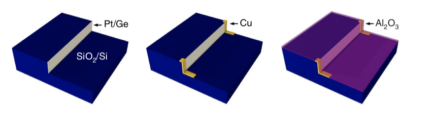
For the manufacture of working memristors, two such blocks are arranged so that the lines are facing each other and form a grid with nine points of intersection. The researchers placed a layer of a mixture of titanium oxide and hafnium oxide with a thickness of 7 nm between the blocks.
Copper wires allow you to activate only one of the three platinum wires in a block at a time. Depending on which of the wires of the opposite block was active, only one intersection is activated.
Thanks for the memory
Under normal conditions, a titanium / hafnium oxide layer would work as an insulator and block the current at the intersections of the copper wires. But when applying a sufficiently strong current, a titanium thread is formed, connecting two pieces of platinum. As a result, a current begins to flow between them; the difference between conducting and isolating states can be considered as the difference between zero and one. The connection maintains its state, unless through it does not apply a sufficiently strong current, which will break the connection.
And it all works. Regarding each intersection of the lattice as a pixel, the authors installed and dropped bits, resulting in a pattern of the letters "NANO".
If the density of their device can be scaled, it will become similar to the three-dimensional flash memory produced in the 64-layer process. This will be 4.5 Tbit per square inch [700 Gbit / sq. cm.]. At the same time, memristors do not need such depth as is necessary for flash memory.
But can it really scale this memory beyond nine bits? Immediately see many potential problems. One of them is the use of platinum. In the plates with a thickness of 11 platinum atoms a bit, and the authors say that they are able to produce them with an efficiency of 100%, but this is still a very expensive material for large-scale production. Therefore, the obvious advantages of finding more common material capable of forming structures with similar properties.
Then comes the production. Processing is comparable to other semiconductor manufacturing, but each step must be repeated by adding additional wire to the device. If you scale it to sizes that give us useful amounts, it can become very time consuming, and rare processing problems can become more serious. If they are rare enough, then you can simply not use defective wires and put up with a reduced amount of memory. This will cut the recording density, but it is already quite high.
Perhaps the most interesting feature of this device is its ability to scale. Although the researchers produced only three parallel wires, each additional wire will drastically increase capacity. The fourth wire will increase the capacity from 9 bits to 16, and the fifth to 25. And if the distance between the wires can be as low as 12 nm, scaling will not lead to significant increases in volume and material consumption.
Source: https://habr.com/ru/post/431532/
All Articles