We write the FPGA loader in LabVIEW. Part 2
Download configuration to FPGA via USB or disassemble FTDI MPSSE
We write the FPGA loader in LabVIEW. Part 1

In the first article, we run into the loading algorithm on the good old C, in the second article, we figured out how to organize a program in LabVIEW and implement a simple user interface. This time we will get acquainted with new methods of work in LabVIEW, analyze the error handling features and complete the project: we will implement the protocol for loading the configuration file into the FPGA.
Error processing
We open the source code, analyze the function MPSSE_open. Despite the algorithmic simplicity (functions are called for each other), quite a lot of D2XX API elements are required: FT_OpenEx , FT_ResetDevice , FT_Purge , FT_SetUSBParameters , FT_SetChars , FT_SetTimeouts , FT_SetLatencyTimer , FT_SetFlowControl , FT_SetBitMode , FT_Purge , FT_SetUSBParameters , FT_SetChars , FT_SetTimeouts , FT_SetLatencyTimer , FT_SetFlowControl , FT_SetBitMode As shown in the previous article , functions are imported using the Call library Function node. This node has dedicated terminals for error control. There is one simple rule in LabVIEW: all VIs must track errors and report errors returned by the terminals errors. Most embedded VP strictly follows it. I hope everyone understands how important it is to monitor and handle errors, especially at the debugging stage, but there is another reason why this is so important, not obvious to "classical" programmers. LabVIEW does not have a strict sequence of instrument execution on the block diagram: the instrument is executed when data are available at its inputs. If from the output of one VP the data is transmitted to the input of another VI, then it is clear that at the beginning the first VI will work, only after it the second. And what if there is no data transfer, and the VIs perform independent actions? Of course, you can use the cumbersome "Flat Sequence Structure", but it is much more convenient to connect devices with each other by a stream of errors.
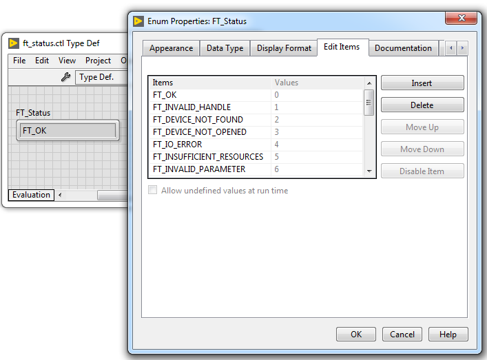
When importing D2XX functions, we encounter two types of errors. The first - this is an error directly imported - returns the block Call library Function . The second is the error of the library itself, returned by almost every function via FT_STATUS . All possible values are described as enum in the ftd2xx.h header file. Although it is enough to know that the value of FT_OK is the absence of an error, and all other values are error codes, I would like to track not only the fact of the error, but also what error occurred and exactly where it occurred.
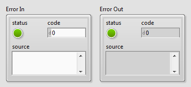
In LabVIEW, error data is propagated through error clusters. This is such a special dedicated data type, LabVIEW has a lot of VIs and functions for working with it. The error cluster consists of three elements: a logical variable — it displays the status, a signed integer number — the error code, and a string — the source of the error. The status indicates whether an error occurred, the error code determines its type and is used by special VIs to generate a report. The line gives a more detailed idea of exactly where the error occurred. In LabVIEW, if the status is TRUE , then this is an error, if the status is FALSE , but the code is not zero and the description string is not empty, then this warning , if the status is FALSE , the code is zero and the string is empty - there is no error.
')
LabVIEW contains an internal database in which each error code is associated with its description. For each type of error, a special range of code values is allocated. For example, for the errors associated with the network operation, several ranges are allocated: from –2147467263 to –1967390460, from 61 to 65, from 116 to 118 and 122, 1101, 1114, 1115, 1132 to 1134, from 1139 to 1143 and from 1178 to 1185 For user-defined errors, two ranges from –8999 to –8000 and from 5000 to 9999 are reserved. From these ranges, we can choose values for the error codes of the D2XX library.
Create a VI that accepts the status of the D2XX function as an input and converts this status into a LabVIEW error cluster. Most functions and VIs in LabVIEW, having received the Error In status TRUE , do not execute their code, but transmit error information to the Error Out terminal. This allows you to effectively transfer information about the source through the entire chain to the error handler, eliminating the execution of code in emergency mode. It is desirable that our VP behaves similarly.
Let's make a list of D2XX statuses in the form of enum and render it into a separate type (in the previous article we did this with the FTDI types).
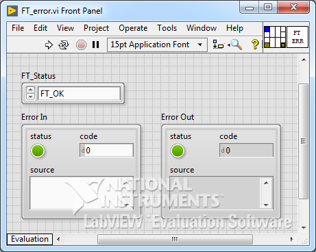
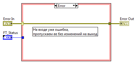
The new VI is saved as FT_error.vi. Two Error In and Error Out clusters are added to the front panel, you can find them in the "Array, Matrix & Cluster" palette. We connect them to the terminals in the connections panel in the lower left and lower right corners, respectively, as was mentioned in the previous article, this is the location of the error stream terminals in LabVIEW. Add a Case structure to the block diagram, Case selector input an Error In cluster, then the Case structure changes color and two subdiagrams divide: "No Error" - green, and "Error" - red. Inside the Error case, we pass an error cluster from the selector terminal directly to the output tunnel on the right border. And in the green case, we add another Case , depending on the status it will determine whether to create an error (status is not FT_OK), or leave it as it is: skip the input error cluster to the output without changing.
In order to technically convert the error code into a cluster, you can use the Error Cluster From Error Code VI . This SubVI adds a call chain to the error description, so that we can determine not only what happened, but also where it happened.
To select the text corresponding to the input status (FT_Status), use the property block: select "RingText.Text". Error text is passed to the input error message VP Error Cluster From Error Code VI .
Do not forget to draw the "talking" icon.
Front (front) sub-instrument panel
Block diagram Error input
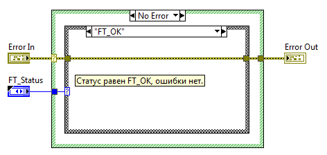
Block diagram There is no error at the input and the status is FT_OK
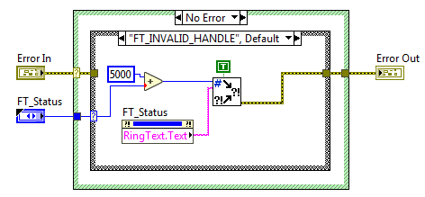
Block diagram There is no error at the input, but the status is different from FT_OK
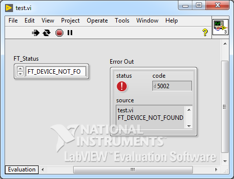
For the FT_error test, you can create an empty VI, add the created VI there and see how the value will change at startup if you submit different statuses.
Front (front) panel of the instrument
Block diagram
Now, after any function call from the D2XX API, we will use SubVI FT_error.vi. And the cluster of errors will pass through all the VIs throughout the call hierarchy.
In the top-level VI, we need to decide what to do with the detected error: you can display a message in the dialog box, write it to the report file, ignore it, or just end the application silently. The dialog box is the easiest and most popular way to report errors. And it is also convenient for a novice programmer, since nothing needs to be done. In each VI, the default automatic error handling mode is enabled ( Enable automatic error error handling , located in the Execution category of the Properties VI menu). It works like this: if in some node the output terminal Error Out not connected anywhere, and an error occurs in that node, LabVIEW pauses the execution of the application and displays a dialog box. If the node's Error Out terminal is connected, the error stream propagates as programmed, and no additional action occurs. However, the message window can be called up programmatically, for this you need to use the General Error Handler and Simple Error Handler VIs (located in the "Dialog & User Interface" panel). In this case, information about the error we can use to complete the program. On the block diagram, it looks like this:
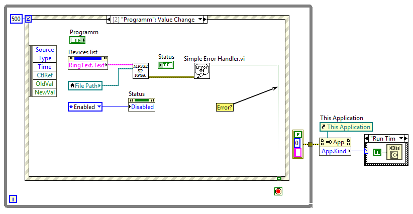
Clickable image
When an error occurs, the program will be paused, a window with a report will appear, after closing the window the program will terminate correctly.
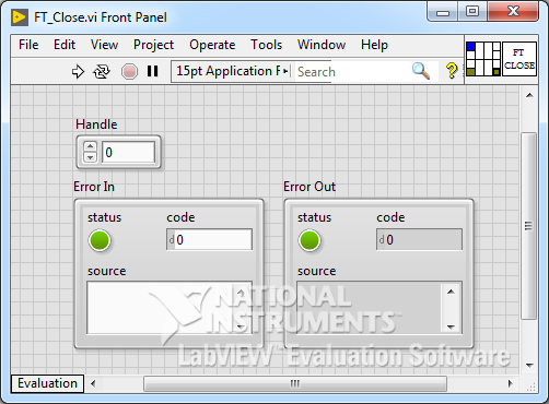
Open and close FTDI
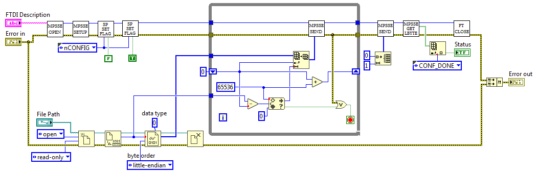
So, back to the MPSSE_open function. Create a new VI . First of all, we add terminals for the error stream. Add a selection structure and feed the selector input Error In . In the green case, we do the import of functions in the order and with the parameters as in the Sishny prototype. All nodes of the Call Library Function Node chained by a stream of errors. In the red case through the tunnel we connect Error In to the output terminal of the error.
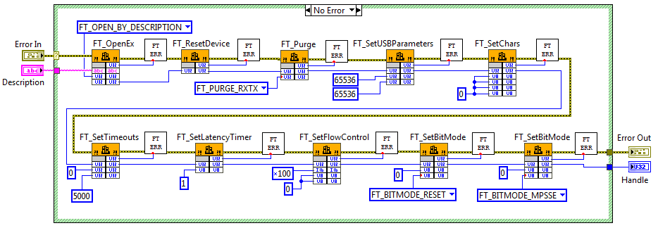
Clickable image

VP MPSSE_open.vi
The input to SubVI is a string describing FTDI ( Description ), the output is Handle and an initialized FTDI chip in MPSSE mode.
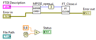
Let's create a VP, completing the work with FTDI and you can already test the performance on the hardware.
Block diagram
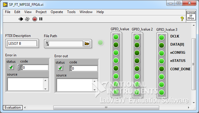
Front Panel
In the previous article for debugging the interface, we made the SP plug SP_FT_MPSSE_FPGA.vi, now it is time to fill it. Add on its block diagram MPSSE_open.vi and FT_Close.vi. At this stage, it is rather difficult to assess whether the initialization was correct, but a nonzero Handle value at the output of MPSSE_open.vi and the absence of an error will tell us a lot.
SP_FT_MPSSE_FPGA.vi block diagram
In order to see the value of Handle you can use the window "Probe Watch Window". This is a handy debugging tool that allows you to display the value of data on any (almost any) wire in the course of instrument execution. In order to install a sample on a line, select the "Probe" item in the context menu of this line itself. The “Probe Watch Window” window will open, and a tsiferka with a sample number will appear on the line. In the picture above it is "3."
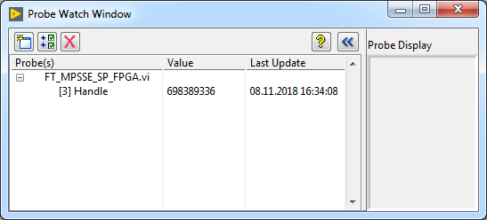
On the line Handle value 698389336
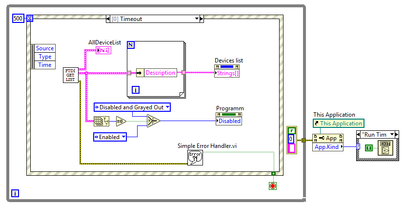
Fine! Run the top-level VI, connect the debugging board to the computer. The description of the connected FTDI chip appears in the "Select device" list, press the "Program" button and ... nothing happens. Only in the "Probe Watch" appeared value Handle . And this is good.
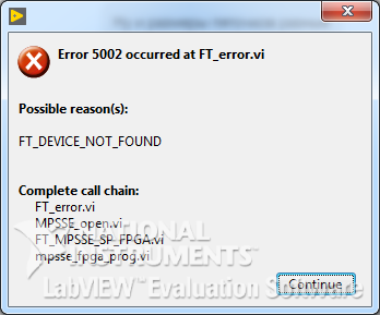
Turning off the board, the list of devices is cleared. Click "Program". This is where the error report window pops up.
After clicking the "Continue" button, the VI ends its work.
It is necessary to prohibit pressing the button if no device is found. Modify the case "Timeout" event handler. Let me remind you that FTDI chips connected to a PC are scanned twice a second, if they are detected and can be used for programming an FPGA, then using the Strings[] property, their descriptors are added to the Devices list . We create the Disabled property for "Program", and if no suitable devices are detected, then disable and dim the button.
The picture is clickable
Mastering GPIO
After MPSSE is activated, it is handled through the so-called "op-code", and from the API functions D2XX, only FT_Write , FT_Read and FT_Queue (to find out the status of the receiver buffer). On the basis of the track, we create the corresponding VI: FT_Write.vi, FT_Read.vi, FT_Queue.vi.
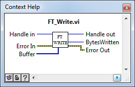
FT_Write.vi
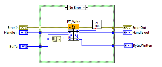
Block diagram FT_Write.vi
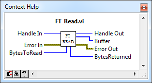
FT_Read.vi
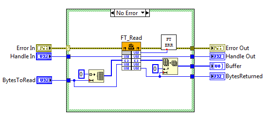
Block diagram FT_Read.vi
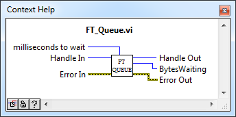
FT_Queue.vi
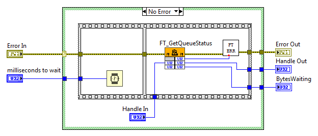
Block diagram FT_Queue.vi
Now from these three bricks lay out the VI for reading the parallel port and writing to it. The value is conveniently represented as an array of Boolean variables.
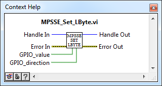
MPSSE_Set_LByte.vi
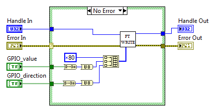
Block diagram MPSSE_Set_LByte.vi
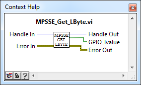
MPSSE_Get_LByte.vi
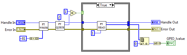
Block diagram MPSSE_Get_LByte.vi
I repent, I was lazy to create a named list for all op-code, so I left them in the form of Magic Numbers.
As mentioned in the very first article, the FPGA "Passive Serial" download protocol is nothing more than SPI with additional flag manipulation. A total of five legs are used: the DCLK , DATA [0] , nCONFIG lines must be configured as outputs, and the nSTATUS and CONF_DONE lines as inputs.
| FPGA pin | Pin name | Pin | MPSSE | Direction | default |
|---|---|---|---|---|---|
| DCLK | BDBUS0 | 38 | TCK / SK | Out | 0 |
| DATA [0] | BDBUS1 | 39 | TDI / DO | Out | one |
| nCONFIG | BDBUS2 | 40 | TDO / DI | Out | one |
| nSTATUS | BDBUS3 | 41 | TMS / CS | In | one |
| CONF_DONE | BDBUS4 | 43 | GPIOL0 | In | one |
We will need a VP, which will be able to change the value on the selected leg without affecting all the others. First of all, we create Enum with the sequence numbers of the legs in the port, save it as "Strict Type Def" to the file SP_LBYTE_BITS.ctl. Create a new VI, add the usual error stream terminals. We read the current value of the parallel port using MPSSE_Get_LByte.vi, using the Replace Array Subset function, we modify the necessary bit and write the value back to the port (MPSSE_Set_LByte.vi).
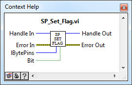
SP_Set_Flag.vi
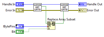
Block diagram SP_Set_Flag.vi
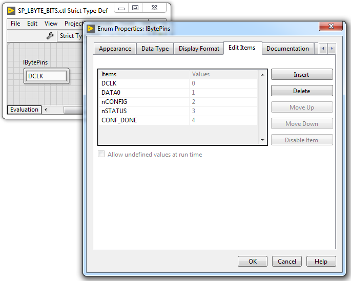
Enum SP_LBYTE_BITS.ctl
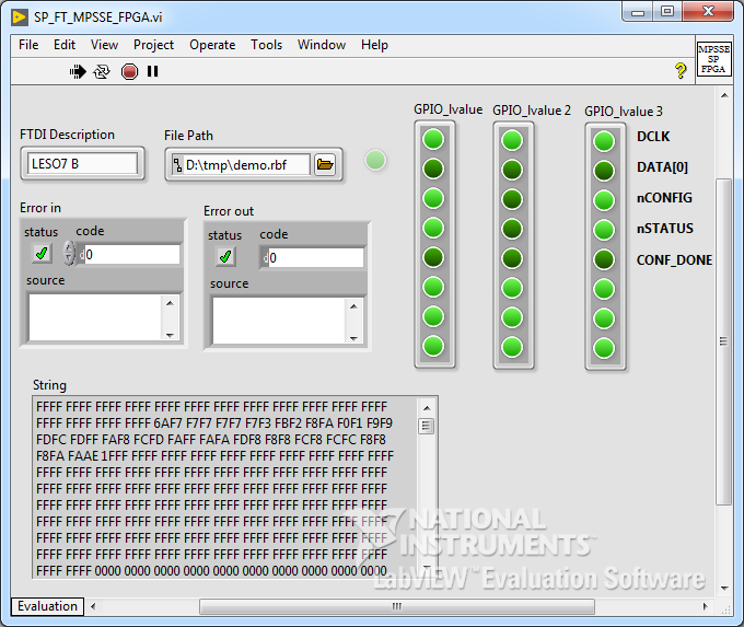
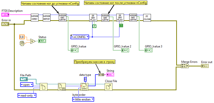
To begin configuration, the MPSSE controller must generate a low-to-high transition on the nCONFIG line. As soon as the FPGA is ready to receive data, it will form a high level on the nSTATUS line. At this stage, everything is ready for an experiment in iron. Add the control of the nCONFIG line to the block diagram SP_FT_MPSSE_FPGA.v - after the initialization of the MPSSE, we submit a low level and then a high one. After each operation (for debugging) we read the state of the port's legs.
During launch
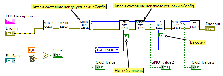
Block diagram
In general, during the launch of the VI, it can be seen that the FPGA responds to the transition on the nCONFIG lines — a zero is set on the nSTATUS pin and then a one. But it will not be superfluous to check it with an oscilloscope. Almost any dual channel oscilloscope with the ability to run on the trigger (standby). Channel A (blue track) I put in the control point of the nCONFIG circuit, channel B (red track) - the chain nSTATUS . The trigger is set to the falling edge of channel A.
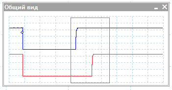
The picture is clickable. With details!
Work with file
FPGA is ready to accept the configuration file. Are we ready to transfer the file to the FPGA?
LabVIEW contains an extensive set of tools for working with files. Not to say that the functional is enough for absolutely the whole range of tasks, but the basic operations like reading and writing are easy and pleasant. The basic set of VI for working with files can be found in the "File I / O" panel. For the problem to be solved, it is necessary to open the configuration file, estimate its size (we need to know how many bytes to send the FPGA), read it and close it. Everything is simple and one after the other. Use the Open/Create/Replace File VI, Get File Size , Read from Binary File , Close File , combine them with an error stream chain and refnum - a number, such as a file descriptor, is created when the file is opened and must be passed to the input by other VIs working with this file.
So far we have nowhere to recycle the read data, but if you really want to check the performance of the chain, then you can create an indicator of the String type and adjust it a little. In the context menu, activate the "Hex Display" option, turn on the vertical scrollbar (Visible Items -> Vertical Scrollbar) and after launching we observe the contents of the binary configuration file.
Front Panel. We look at the contents of the file
Block diagram Karinka clickable
The block diagram of the VP formed two independent parallel lines of code, so separate error chains are used for them. In order to reduce parallel threads into one Error Out terminal, the Merge Errors function is used. This function looks for errors at the input from top to bottom (yes, there may be more than two input terminals, stretched with the mouse) and returns the first one it finds. If there are no errors, it returns the first warning that occurred. If no warnings are detected, then there is no error at the output. It is important to note that the order of connecting inputs Merge Errors determines the priority of errors, and if an error occurs in two chains at once, the lower error will be ignored. To this must be treated carefully.
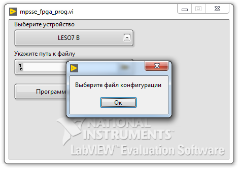
If we try to press the "Program" button in the top-level VI without selecting a file, then SP_FT_MPSSE_FPGA.vi will have a blank path at the input, which will cause the error "Error 1430. LabVIEW: (Hex 0x596) absolute path. " As my childhood friend says: "Trivia, it’s something everyday!" And this mistake is not a mistake at all, but a user's inattention. We will not stop the program and swear at it with a window with a red cross, simply remove the error with this code from the stream and in the dialog box we recommend the user to decide on the file. To filter errors, use the "Clear Errors" VP from the "Dialog & User Interface" palette. To display the message - "One Button Dialog".

The picture is clickable
Loading configuration
For serial data transmission to the MPSSE processor, you need to send op-code 0x18, the command arguments will be the length of the transmitted sequence (two bytes, starting from the low order), and the data sequence itself. Length is coded minus one. Sending a data block will be issued as MPSSE_send.
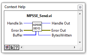
MPSSE_Send.vi
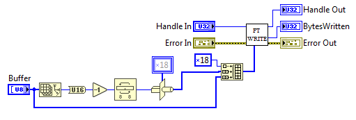
Block diagram
We convert the input buffer size ( Array Size ) to the U16 two-byte type, subtract the unit, swap the low byte and high byte ( Swap Bytes ) - send the length starting from the low byte, and convert the two-byte number to a one-byte array ( Type Cast ).
The Type Cast feature deserves special attention. This is such a universal type converter, the acumen of which is sometimes very surprising. In short, then:
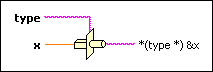
Visually for programmers
However, this is not just a conversion of data to another type, it is also a heuristic interpretation. This function allows you to convert between incompatible data types, and the function does not hesitate to align the input data and even remove the "extra" parts. If the requested data type requires more memory than the input data, the function will allocate the missing amount. For a novice developer, LabVIEW Type Cast can become a lifesaver, but with growing up, it is better to refuse such a converter — it is very much hidden from view and can become a source of unforeseen errors. It is better to use more explicit conversion methods, for example, Coerce To Type .
When initializing the MPSSE processor, we set the maximum allowable buffer size for data transfer to 65536 bytes, hence the configuration file we should divide into fragments whose size does not exceed the specified size. We use the Array Subset function, this function selects subarrays from an array starting with the index element and length . We will split in the While loop, each iteration of the index will be increased by 65536, between iterations we will pass the value through the shift register. As soon as it is not possible to pinch 65536 bytes from the main array, we take everything that is left, we send and stop the cycle.
According to the download protocol, after all the data has been transmitted, you need to submit two more clock pulses in order for the FPGA to initialize. To do this, after the cycle, we are sending another “empty” byte.
The picture is clickable
In order to understand the success of the firmware, we consider the flags, and if CONF_DONE is set to one, we report the top level VI, that everything is OK.
The program is complete. It remains to make sure that the FPGA is successfully flashed, and the board blinks happily with LEDs.
About naming VP
, , LabVIEW, , SubVI. . :
- — , FTDI, API D2XX. "FT", FT_Close.vi FT_Read.vi.
- — MPSSE. "MPSSE". : MPSSE_open.vi, MPSSE_Set_LByte.vi, MPSSE_Get_LByte.vi.
- — "Passive Serial" MPSSE. "S". , SP_FT_MPSSE_FPGA.vi ( , ) SP_LBYTE_BITS.ctl.
- . . , .
( ), . subVI .
Conclusion
, , .
, LabVIEW, . , , , ( ). .
Materials on the topic
- . LabVIEW: . Per. from English by ed. .– .:
, 2008 – 400 .: . - labview_mpsse . .
- .
- Software Application Development D2XX Programmer's Guide . API D2XX.
Source: https://habr.com/ru/post/429448/
All Articles