IBM overcomes the 7 nm barrier using graphene to place nanomaterials on substrates
The functionality of the devices can be changed by simply changing the nanomaterials and without affecting the process.
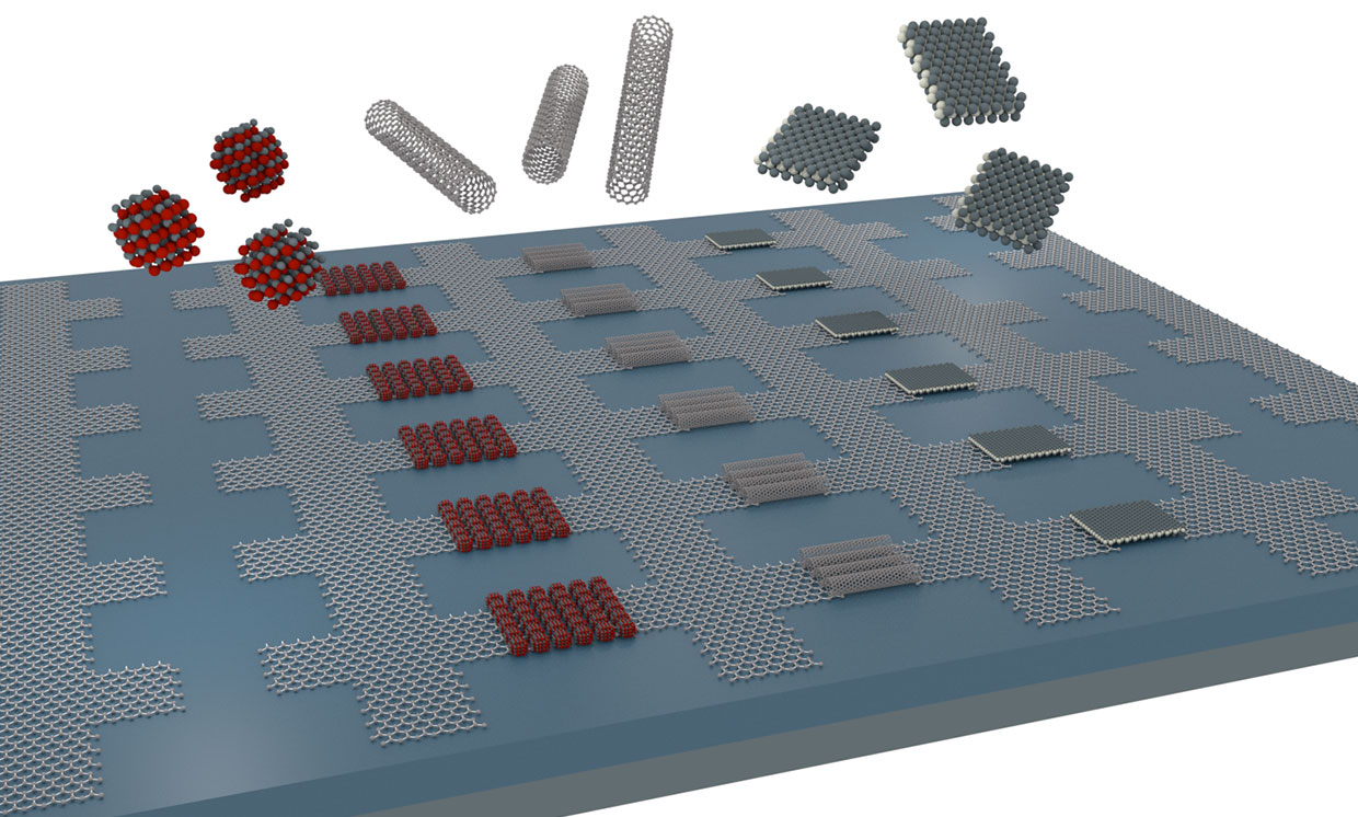
Quantum dots (red), carbon nanotubes (gray), and molybdenum disulfide nanoliths (gray-white) are, respectively, representatives of nanomaterials of classes 0D, 1D, and 2D, which can be collected on a large scale using the graphene-based placement method .
Four years ago, IBM announced that over the next five years, it is going to invest $ 3 billion in the future of nanoelectronics as part of the extensive project “7 nm and beyond” [7nm and Beyond]. At least one of the major chip manufacturers, GlobalFoundries, has rested against the wall of the 7nm process, and IBM is trying to go further, using graphene to place nanomaterials in certain places without chemical pollution.
A study published in the journal Nature Communications described how IBM scientists first electrified graphene in such a way that it helped locate nanomaterials with 97% accuracy.
“Since this method works with a wide variety of nanomaterials, we imagine integrated devices with functionality based on the unique physical properties of nanomaterials,” said Matthias Steiner , manager of the Brazilian branch of IBM Research. "We can also imagine detectors and light emitters on a chip that have a certain wavelength determined by the optical properties of the nanomaterial."
')
As an example, Steiner explained that if you need to change the spectral properties of an optoelectronic device, you can simply replace the nanomaterial, leaving the rest of the production process unchanged. If we continue the development of this method even further, it will be possible to assemble different nanomaterials in different places in several passes of the assembly line, and create light detectors operating in different frequency windows at the same time. "
The process can be described as a hybrid, unifying “top-down” [top-down] and “bottom-up” [bottom-up] approaches , according to Michael Ingel , a member of the Brazilian research team. A couple of years ago, IBM created one of these hybrid processes that combined top-down manufacturing technologies — such as lithography — with bottom-up technologies that “grow” electronics through self-assembly.
Ingel explained that the first step of the hybrid process is growing graphene directly on the substrate on which the nanomaterial is being assembled. In a demonstration by the company, graphene on silicon carbide was used. Ingel noted that it is also possible to grow graphene on other materials, for example, on copper, and then peel it off and place it on a substrate of silicon or silicon oxide.
The next step is etching graphene to locate. This is done on a large scale and can be considered part of the process from the top-down technology.
In the third step, a bottom-up technology is used, in which researchers place graphene layers in an alternating electric field, while simultaneously placing the nanomaterial solution on top. Nanomaterial seeps down and is between opposite graphene electrodes.
“So graphene determines the location and provides the orientation of the electric field and the force pulling in the nanomaterial for its directional assembly,” said Ingel.
At the fourth step, the graphene electrodes are etched, and additional manufacturing operations are carried out to integrate electronics or optoelectronic devices.
Prior to this, the most advanced method was the use of metal electrodes, which are difficult to remove, and which limit the efficiency of the device and the potential for integration. “We believe that the biggest breakthrough in this work is the bottom-up arrangement of a wide range of nanomaterials with a resolution of nanometer scales on where as larger areas of millimeter size and with easily removable electrodes,” said Steiner. “Graphene electrodes provide excellent alignment and density of the nanomaterial, limit interaction with chemicals, and avoid metal lines, which results in superior device efficiency.”
This process will not be able to quickly help the implementation of Moore's law . One of the biggest problems, according to Ingel, is the use of nanomaterial solutions in industrial scale production. “This will require progress on the standardization of nanomaterial solutions in order to achieve repeatable and permanent results, as well as adapting the method with an auxiliary electric field to use in substrates manufacturing processes,” said Ingel.
And although IBM will not decide on the standardization of nanomaterials, researchers continue to work on technology, integrating various nanomaterials in order to modify integrated circuits such as, for example, electrical inverters or ring generators, according to different requirements. Also, researchers are developing light emitters and detectors on a chip, the spectral properties of which are determined by the nanomaterial used.
Source: https://habr.com/ru/post/427329/
All Articles