My “Hello World!” On FPGA or the next version of UART

Finally, I got around to exploring the FPGA. But somehow it turns out to be wrong: I’m writing drivers for hardware for Linux, I program microcontrollers, I read the circuits (and project a little), I have to grow further.
Since it did not seem interesting to flash the LEDs, I decided to do a simple thing. Namely, write receiver and transmitter modules for UART, integrate them inside the FPGA (at the same time understand how to use IP Core), and test it all on real hardware.
Immediately I say that the universal parametrized core of the task was not done. This is just a test project, on the subject of "feeling what a FPGA is and how to communicate with it."
So let's start with the receiver. The algorithm is described quite well , so I will repeat here only its main points.
')
- The sampling frequency of the RX signal is four times higher than the required UART transmission rate.
- The condition for the start of reception will be considered the transition of the input signal RX from a high level to a low one if it is not being received at the moment.
- The condition for the reliable identification of the start bit will be considered to be the holding of the RX signal in the low level state on the second clock of the sampling frequency. At the same time, we practically fall into the middle of a bit pulse, which will allow us to further perform sampling of pulses every 4 clock cycles.
- In case of an error in the start bit or in the stop bit, set the error signal error. Based on it, we form the fastsync signal, which we will use in the future to quickly synchronize the receiver.
- After recognizing the start bit, we begin the sequential reception of data bits, starting with the youngest. The received data is written to the register with a shift to the right by one bit. The condition for the end of reception will be the detection of the start bit in the 0th position of the shift register.
- Fast synchronization of the receiver consists in bringing it back to its original state after an error is detected when the RX signal goes to a high level (this can be either a transmission of a logical "1" or a transmission of a stop bit or an idle state of the transmission line).
- The condition for successful completion of reception (correct values of the start and stop bits) is the complete signal. From it (when clocked by the rdclk signal) a pulse signal is prepared, which indicates the presence of valid data on the rxdata bus.
Immediately, I note that I did not want to clock the read signal from the clock signal clk (unexpectedly, yes?), So as not to tie up the speed of subsequent data processing to the UART exchange rate. A similar implementation in the transmitter module ( see below ). A test bundle of receiver and transmitter modules is made on the basis of Intel's IP Core FIFO, moreover, with the ability to simulate different speeds for the consumer and the data generator. The only limitation is that the clock frequency of the producer and the data consumer must not be lower than the clock frequency clk.
Receiver Module (Verilog)
// // UART // // rxdata , ready==1 error==0. // ready 1 rdclk. // // : // rx // 2- . , . // 8 - ( 9 ). // 2 - , // . // // . // . '0' , . '1' // idle (. '1') // start- (. '0') // stop- (. '1') module uart_rx( nreset, // (, 0) clk, // UART, .. UART rx, // UART rdclk, // (rxdata, ready) rxdata, // , ready==1 ready, // rxdata ( 1) error, // ( 1) busy, // ( , 1) idle); // ( 1) input wire nreset; // (, 0) input wire clk; // , .. UART input wire rx; // UART input wire rdclk; // output wire[7:0] rxdata; output wire ready; output error; output busy; output idle; // , rdclk reg[2:0] done = 3'b000; // , rdclk //assign ready = (done == 2'b10) ? 1'b1 : 1'b0; assign ready = (done[1] && !done[0]) ? 1'b1 : 1'b0; // reg error = 1'b0; // // error // rx, . wire fastsync = (error && rx); // reg idle = 1'b1; // : // d[9] - , .. == 1 // d[8:1] - // d[0] - , .. == 0 reg[9:0] d = 10'b1xxxxxxxx1; // . 2'b10 wire[1:0] status = { d[9], d[0] }; // . wire complete = (status == 2'b10) ? 1'b1 : 1'b0; // assign rxdata = d[8:1]; // reg busy = 0; // rx reg[1:0] cnt; always @(posedge clk, negedge nreset) begin if(!nreset) begin rxreset(); end else begin if(fastsync) begin rxreset(); end else begin if(busy == 1'b1) begin // -, rx if(cnt == 2'd0) begin // // // (.. ) d <= { rx, d[9:1] }; if(d[1] == 1'b0) begin // , busy <= 1'b0; // error <= (rx == 1'b1) ? 1'b0 : 1'b1; end else begin // if(rx && (d == 10'b1111111111)) begin // busy <= 1'b0; // error <= 1'b1; end else begin // // - - cnt <= 2'd3; end end end else begin // - cnt <= cnt - 2'd1; end end else begin // if(!error) begin // , if(rx == 1'b0) begin // - busy <= 1'b1; // . 1, .. // d[0]==0 d <= 10'b1111111111; // rx 1/2 // 1- - // 2- - (cnt 0) cnt <= 2'd0; // .. , idle <= 1'b0; end else begin // idle <= 1'b1; end end end end end end task rxreset; begin // error <= 1'b0; // (!?) idle <= 1'b1; // busy <= 0; // -, complete d <= 10'b1xxxxxxxx1; end endtask always @(negedge rdclk, negedge nreset) begin if(!nreset) begin done <= 3'b000; end else begin // complete. // ready // complete 0 1 rdclk. done <= { complete, done[2:1] }; end end endmodule Since the RX input signal is asynchronous and (possibly) unstable, a major element was connected in front of the receiver module in the main module . The element is also written in Verilog, but it makes no sense to give its code here. Instead, a beautiful picture of the synthesized element.
Synthesized Majority Element Scheme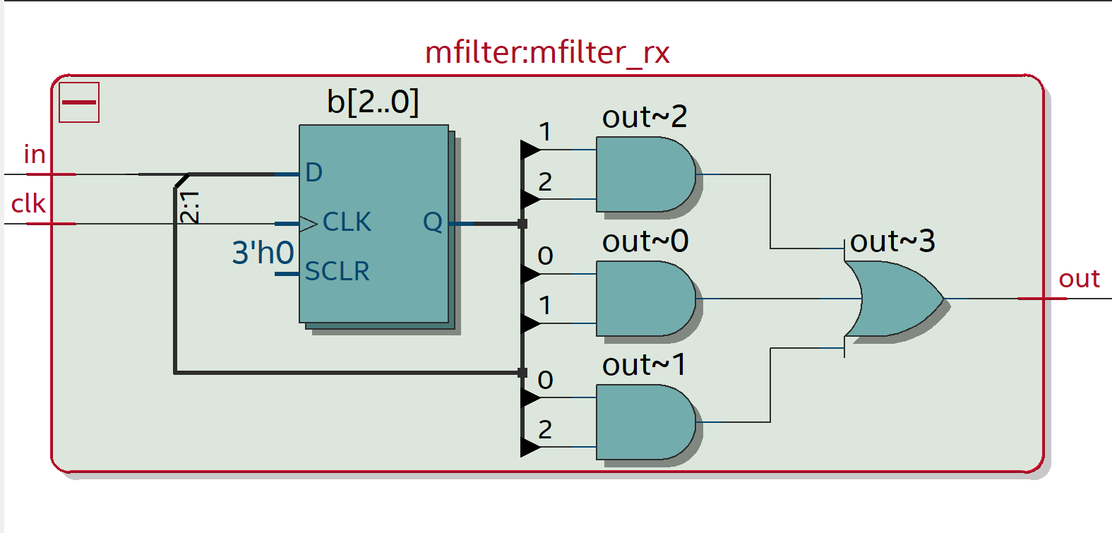
The transmitter unit is even simpler and, I hope, does not need additional comments.
Transmitter module (Verilog, blocking and non-blocking assignments inside always)
// // UART // // : // clk - 4 , // rdclk - txdata, write, fetch. .. clk // txdata - , write/fetch // write - (1=) // fetch - (1=) // tx - UART // idle - (1=, ) // // FIFO dcfifo_component.lpm_showahead = "ON" module uart_tx( nreset, // (, 0) clk, // UART, .. UART rdclk, // txdata, // write, // ( 1) idle, // ( 1) fetch, // , rdclk tx); // UART input wire nreset; // (, 0) input wire clk; // UART input wire rdclk; input wire[7:0] txdata; input wire write; output wire idle; output fetch; output tx; // reg tx = 1'b1; reg fetch = 1'b0; // 4 reg[1:0] div4 = 2'd0; // : reg[3:0] s = 4'd10; // assign idle = (s == 4'd10); // reg[7:0] d; // reg sendstart; // reg canfetch; // , clk reg gotdata = 1'b0; // clock domains reg[2:0] sync = 3'b000; // rdclk write reg wr = 1'b0; // getdata==1 // nextdata // gotdata==1. , // . // gotdata getdata. always @(posedge rdclk, negedge nreset) begin if(!nreset) begin wr <= 1'b0; sync <= 3'b000; // fetch <= 1'b0; end else begin // write wr <= write; // sync <= { gotdata, sync[2:1] }; // gotdata // . // . fetch <= (sync[1] && !sync[0]) ? 1'b1 : 1'b0; end end always @(posedge clk, negedge nreset) begin if(!nreset) begin // div4 <= 2'd0; s <= 4'd10; gotdata <= 1'b0; end else begin // sendstart = 1'b0; // canfetch = wr; if(div4 == 2'd0) begin case(s) 4'd0: begin // sendstart = 1'b1; // , canfetch = 1'b0; end 4'd9: begin // tx <= 1'b1; end 4'd10: begin // idle, end default: begin // , tx <= d[0]; // d <= { 1'b0, d[7:1] }; // , canfetch = 1'b0; end endcase end else begin // div4 <= div4 - 2'd1; if(s < 4'd9) begin // 9 ! canfetch = 1'b0; end end if(canfetch) begin // , d <= txdata; // gotdata <= 1'b1; if(idle /*s == 4'd10*/) begin // idle - sendstart = 1'b1; end else begin // s <= 4'd0; end end if(gotdata) begin // , gotdata <= 1'b0; end if(sendstart) begin // tx <= 1'b0; // s <= 4'd1; // div4 <= 2'd3; end else begin if(div4 == 2'd0) begin if(s < 4'd10) begin // s <= s + 4'd1; // div4 <= 2'd3; end end end end end endmodule The above implementation of the transmitter caused a heated discussion in the comments. Although as a result, it seems everyone agreed that you can do this, but be careful. For your own peace of mind, the module has been rewritten to reflect all the mentioned guideliness. In my opinion, it is not much more complicated than the previous one in terms of human perception of the implemented algorithm.
Transmitter Module (Verilog, ideologically correct)
// // UART // // : // clk - 4 , // rdclk - txdata, write, fetch. .. clk // txdata - , write/fetch // write - (1=) // fetch - (1=) // tx - UART // idle - (1=, ) // // FIFO dcfifo_component.lpm_showahead = "ON" module uart_tx( nreset, // (, 0) clk, // UART, .. UART rdclk, // txdata, // write, // ( 1) idle, // ( 1) fetch, // , rdclk tx); // UART input wire nreset; // (, 0) input wire clk; // UART input wire rdclk; input wire[7:0] txdata; input wire write; output wire idle; output fetch; output tx; // reg tx = 1'b1; reg fetch = 1'b0; // 4 reg[1:0] div4 = 2'd0; // : reg[3:0] s = 4'd10; // assign idle = (s == 4'd10); // reg[7:0] d; // reg sendstart; // reg canfetch; // , clk reg gotdata = 1'b0; // clock domains reg[2:0] sync = 3'b000; // rdclk write reg wr = 1'b0; // getdata==1 // nextdata // gotdata==1. , // . // gotdata getdata. always @(posedge rdclk, negedge nreset) begin if(!nreset) begin wr <= 1'b0; sync <= 3'b000; // fetch <= 1'b0; end else begin // write wr <= write; // sync <= { gotdata, sync[2:1] }; // gotdata // . // . fetch <= (sync[1] && !sync[0]) ? 1'b1 : 1'b0; end end // (?) always // sendstart canfetch always @(*) begin // sendstart = 1'b0; if(nreset) begin // canfetch = wr; if(div4 == 2'd0) begin case(s) 4'd0: begin // sendstart = 1'b1; // , canfetch = 1'b0; end 4'd9: begin // end 4'd10: begin // idle, end default: begin // // , canfetch = 1'b0; end endcase end else begin if(s < 4'd9) begin // 9 ! canfetch = 1'b0; end end if(canfetch && idle) begin // idle - sendstart = 1'b1; end end else begin // reset canfetch = 1'b0; end end always @(posedge clk, negedge nreset) begin if(!nreset) begin // div4 <= 2'd0; s <= 4'd10; gotdata <= 1'b0; end else begin if(div4 == 2'd0) begin case(s) 4'd0: begin // sendstart end 4'd9: begin // tx <= 1'b1; end 4'd10: begin // idle, end default: begin // , tx <= d[0]; // d <= { 1'b0, d[7:1] }; end endcase end else begin // div4 <= div4 - 2'd1; end if(canfetch) begin // , d <= txdata; // gotdata <= 1'b1; if(!idle /*s == 4'd10*/) begin // s <= 4'd0; end end else begin // , gotdata <= 1'b0; end if(sendstart) begin // tx <= 1'b0; // s <= 4'd1; // div4 <= 2'd3; end else begin if((div4 == 2'd0) && (s < 4'd10)) begin // s <= s + 4'd1; // div4 <= 2'd3; end end end end endmodule To test the receiver and transmitter, a main module was written on the lap. I ask him not to swear, design errors (external asynchronous signal nreset, no FIFO reset, etc.) I myself know. But for the purposes of testing the functionality they are not essential.
My demo board is clocked from a 50Mhz signal source. Therefore, in the main module I used a PLL, at the output of which C0 I formed a frequency for operation with UART (1.8432Mhz, really 1.843198Mhz) and, as a joke, I formed a frequency of 300Mhz (output c1 PLL) for timing the simulation of the information processing circuit.
Main module (Verilog)
// // .. UART UART, // FPGA, // FIFO IP CORE DCFIFO. // //NB! // SDC- ! // ( if , // ). module uart( input wire clk50mhz, // 50Mhz input wire nreset, // input wire rx, // UART output wire tx, // UART output wire overflow ); // 1.8432Mhz ( 1.843198Mhz) wire clk_1843200; // 1.2288Mhz ( 1.228799Mhz) //wire clk_1228800; // 300Mhz, PLL wire clk300mhz; // UART uart_pll pll50mhz(.inclk0(clk50mhz), .c0(clk_1843200) /*, .c1(clk_1228800)*/, .c1(clk300mhz)); // UART 38400 // (1843200/38400)/4 = 12 ('b1100). // UART 57600 // (1843200/57600)/4 = 8 // UART 115200 // (1843200/115200)/4 = 4 // UART 230400 // (1843200/230400)/4 = 2 // UART 460800 // (1843200/460800)/4 = 1 (.. !) // UART wire uart_baud4; // // .data 1 . // uart_baud4 .clock/ // uart_baud4 .clock uart_osc uart_osc_1(.clock(clk_1843200), .data(5'd2/*5'd4*//*5'd12*/-5'd1), .sload(uart_baud4), .cout(uart_baud4)); //wire uart_baud4 = clk_1843200; // wire rxf; // mfilter mfilter_rx(.clk(clk50mhz /*clk_1843200*/), .in(rx), .out(rxf)); //wire rxf = rx; // wire[7:0] rxdata; wire rxready; wire error; uart_rx uart_rx_1(.nreset(nreset), .clk(uart_baud4), .rx(rxf), .rdclk(clk300mhz /*clk50mhz*/ /*clk_1843200*/), .rxdata(rxdata), .ready(rxready), .error(error)); wire[7:0] txdata; // , , wire txnone; // , wire fetch; wire full; // // uart_baud4 // clk50mhz uart_fifo_rx uart_fifo_rx_1(.data(rxdata), .rdclk(clk300mhz /*clk50mhz*/ /*clk_1843200*/ /*uart_baud4*/), .rdreq(fetch), .wrclk(clk300mhz /*clk50mhz*/ /*clk_1843200*/ /*uart_baud4*/), .wrreq(rxready), .rdempty(txnone), .q(txdata), .wrfull(full)); assign overflow = ~error; uart_tx uart_tx_1(.nreset(nreset), .clk(uart_baud4), .rdclk(clk300mhz /*clk50mhz*/ /*clk_1843200*/), .txdata(txdata), .write(~txnone), .fetch(fetch), .tx(tx)); endmodule For testing, a testcom traffic generator from Zelax was used. Unfortunately, my USB / UART adapter I had refused to work at speeds above 230400BPS, so all testing was done at this speed.
Test result with RX input filtering using major element
Signal Tap State
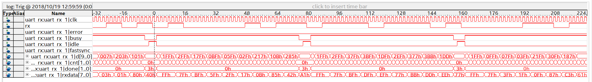
Signal Tap State
And here the majority element was removed from the entrance.
And what, how could I still imitate arbitrary errors when checking the fast synchronization scheme?

Signal Tap State
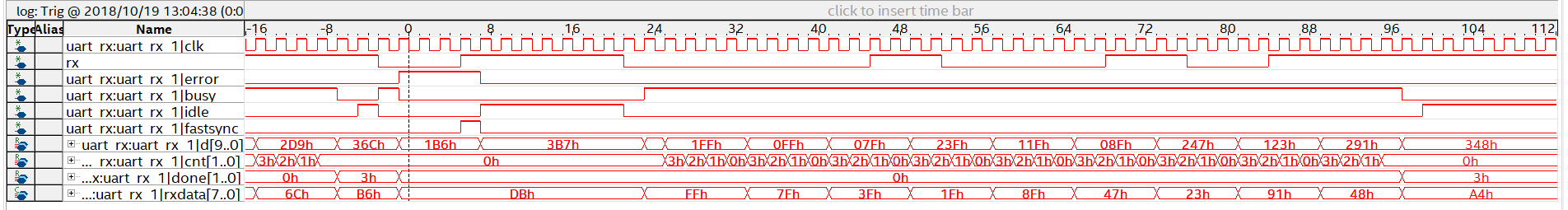
Signal Tap State
Note
Sorry, I did not take courses on Quartus and there was no one to ask questions. I stumbled on it myself and warned about other novice FPGAs: be sure to create an SDC file in the project and describe the clock frequencies in it. Yes, the project is going on without it, though it is possible that warnings may appear if the synthesizer could not determine the timing characteristics. I first ignored them until I killed half a day to determine the problem, why I have a receiver module when I execute the code
if(rx == 1'b0) begin busy <= 1'b1; d <= 10'b1111111111; cnt <= 2'd0; idle <= 1'b0; end else begin the busy and idle signals were set correctly, but the contents of register d sometimes did not change.
Appendix: SDC file for the project
set_time_format -unit ns -decimal_places 3 # 50Mhz, (50/50 duty cycle) create_clock -name {clk50mhz} -period 20.000 -waveform { 0.000 10.000 } ############################################################################## Now that we have created the custom clocks which will be base clocks,# derive_pll_clock is used to calculate all remaining clocks for PLLs derive_pll_clocks -create_base_clocks derive_clock_uncertainty # PLL ? # altpll_component.clk0_divide_by = 15625, # altpll_component.clk0_duty_cycle = 50, # altpll_component.clk0_multiply_by = 576, # altpll_component.clk0_phase_shift = "0", #create_generated_clock -name clk_1843200 -source [get_ports {clk50mhz}] -divide_by 15625 -multiply_by 576 -duty_cycle 50 -phase 0 -offset 0 # baudrate=38400 # 1/4 , .. duty=(1/4)*100=25% #create_generated_clock -name uart_baud4 -source [get_nets {pll50mhz|altpll_component|auto_generated|wire_pll1_clk[0]}] -divide_by 12 -duty_cycle 25 [get_nets {uart_osc_1|LPM_COUNTER_component|auto_generated|counter_reg_bit[0]}] # baudrate=230400 # 1/4 , .. duty=(1/4)*100=50% create_generated_clock -name uart_baud4 -source [get_nets {pll50mhz|altpll_component|auto_generated|wire_pll1_clk[0]}] -divide_by 2 -duty_cycle 25 [get_nets {uart_osc_1|LPM_COUNTER_component|auto_generated|counter_reg_bit[0]}] # baudrate=460800 # 1, PLL, . | altpll_component | auto_generated | wire_pll1_clk [ set_time_format -unit ns -decimal_places 3 # 50Mhz, (50/50 duty cycle) create_clock -name {clk50mhz} -period 20.000 -waveform { 0.000 10.000 } ############################################################################## Now that we have created the custom clocks which will be base clocks,# derive_pll_clock is used to calculate all remaining clocks for PLLs derive_pll_clocks -create_base_clocks derive_clock_uncertainty # PLL ? # altpll_component.clk0_divide_by = 15625, # altpll_component.clk0_duty_cycle = 50, # altpll_component.clk0_multiply_by = 576, # altpll_component.clk0_phase_shift = "0", #create_generated_clock -name clk_1843200 -source [get_ports {clk50mhz}] -divide_by 15625 -multiply_by 576 -duty_cycle 50 -phase 0 -offset 0 # baudrate=38400 # 1/4 , .. duty=(1/4)*100=25% #create_generated_clock -name uart_baud4 -source [get_nets {pll50mhz|altpll_component|auto_generated|wire_pll1_clk[0]}] -divide_by 12 -duty_cycle 25 [get_nets {uart_osc_1|LPM_COUNTER_component|auto_generated|counter_reg_bit[0]}] # baudrate=230400 # 1/4 , .. duty=(1/4)*100=50% create_generated_clock -name uart_baud4 -source [get_nets {pll50mhz|altpll_component|auto_generated|wire_pll1_clk[0]}] -divide_by 2 -duty_cycle 25 [get_nets {uart_osc_1|LPM_COUNTER_component|auto_generated|counter_reg_bit[0]}] # baudrate=460800 # 1, PLL, . | counter_reg_bit [ set_time_format -unit ns -decimal_places 3 # 50Mhz, (50/50 duty cycle) create_clock -name {clk50mhz} -period 20.000 -waveform { 0.000 10.000 } ############################################################################## Now that we have created the custom clocks which will be base clocks,# derive_pll_clock is used to calculate all remaining clocks for PLLs derive_pll_clocks -create_base_clocks derive_clock_uncertainty # PLL ? # altpll_component.clk0_divide_by = 15625, # altpll_component.clk0_duty_cycle = 50, # altpll_component.clk0_multiply_by = 576, # altpll_component.clk0_phase_shift = "0", #create_generated_clock -name clk_1843200 -source [get_ports {clk50mhz}] -divide_by 15625 -multiply_by 576 -duty_cycle 50 -phase 0 -offset 0 # baudrate=38400 # 1/4 , .. duty=(1/4)*100=25% #create_generated_clock -name uart_baud4 -source [get_nets {pll50mhz|altpll_component|auto_generated|wire_pll1_clk[0]}] -divide_by 12 -duty_cycle 25 [get_nets {uart_osc_1|LPM_COUNTER_component|auto_generated|counter_reg_bit[0]}] # baudrate=230400 # 1/4 , .. duty=(1/4)*100=50% create_generated_clock -name uart_baud4 -source [get_nets {pll50mhz|altpll_component|auto_generated|wire_pll1_clk[0]}] -divide_by 2 -duty_cycle 25 [get_nets {uart_osc_1|LPM_COUNTER_component|auto_generated|counter_reg_bit[0]}] # baudrate=460800 # 1, PLL, . Many thanks to everyone who wrote comments on the article! Of these, I drew a lot of useful, although sometimes somewhat contradictory information. In my opinion, their value is much greater than the implementation of the algorithm described above. And, undoubtedly, they will be useful to those who also dare to climb into the world of FPGAs.
List of external links
Source: https://habr.com/ru/post/427011/
All Articles