Electron "walking": charge manipulations inside the structure of unsaturated bonds

The devil is in the details. This phrase can very briefly and accurately describe the process of finding new building blocks of modern technology. After all, even nuclear weapons with all its destructive power created on the basis of the processes occurring at the atomic level. Today we will be acquainted with research that also affects atoms, but not for using them for destruction, but for creation. Namely, about the management of electrons and their behavior, which will help the development of quantum computing technologies and artificial neural networks. As scientists managed, so to speak, to put an electron on a leash and walk it along a given path, we learn from their report. Go.
The basis of the study
Over the past few years, there has been far from a single study of manipulations with electrons, their properties, behavior, and state. Many scientists consider this direction to be very promising, others call it so fundamentally important for future technologies. In this case, a natural question arises - how does this study differ from its predecessors? Researchers give a fairly clear answer - the bias voltage. Previous studies relied on it, achieving control over the electron, more precisely, on the charge transfer process. Thus, an insignificant tunneling current was achieved, and charge manipulations were carried out by transferring individual electrons.
')
In the case of today's research, the procedure has been changed. Scientists managed to gain control over the charge inside the atomic nanostructure based on one-electron events, but without the need to apply a bias voltage.
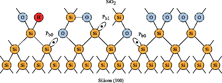
An example of silicon unsaturated bonds
Silicon unsaturated bonds (hereinafter referred to as NS) on the Si (100) -2x1 surface passivated by hydrogen became the material basis for the study. Scientists note that the use of silicon has certain advantages. The main thing is the electronic isolation of unsaturated bonds from the substrate, which allows them to localize the charge without the use of a thin layer of insulator between the main structure and the substrate. The use of an insulating layer has often been applied previously. Here we found another difference of the current study from its predecessors. But the exact intervals between the NA were obtained by the crystal lattice.
As mentioned earlier, other researchers have applied bias voltages or even charged NSs to bias the charge. Immediately approach more mechanical. It consists in using a probe that directly manipulates the equilibrium position of an atom, which allows this atom to become a carrier of a negative charge. Thus, the absence of a bias voltage and the short-range interaction between the probe and the atom make it possible to achieve control over an individual electron.
Conducting experiments
The main instrument of this study was the Omicron LT atomic force / tunneling microscope operating at a temperature of 4.5 K and ultrahigh vacuum (<1 x10 -10 Torr).

Omicron LT Microscope
The microscope needles were made of polycrystalline tungsten wire, which was chemically etched, sharpened with a focused ion beam and attached to the qPlus sensor.
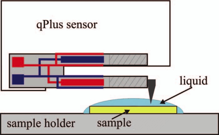
QPlus sensor circuit
The needle resonance frequency was 28 kHz, the quality factor was in the range of 12 ... 14, and the amplitude was 50 picometers. An additional electrode on the sensor was also used to provide tunneling current. In addition, the needles were sharpened with nitrogen etching during ion microscopy.
During the study itself, the needle touched the surface of the sample, as a result, silicon atoms remained at the tip of the needle.
The working sample itself was made of high-doped (1.5 × 10¹⁹ atoms / cm3) (100) Si crystals. Then the process of degassing was carried out at a temperature of 600 ° C for 12 hours, annealed with a maximum temperature of 1250 ° C, and then passivation with hydrogen at a temperature of 330 ° C.
Unsaturated bonds were formed by applying short voltage pulses (+2.1 V, 10 ms) when the needle was located directly above the hydrogen.
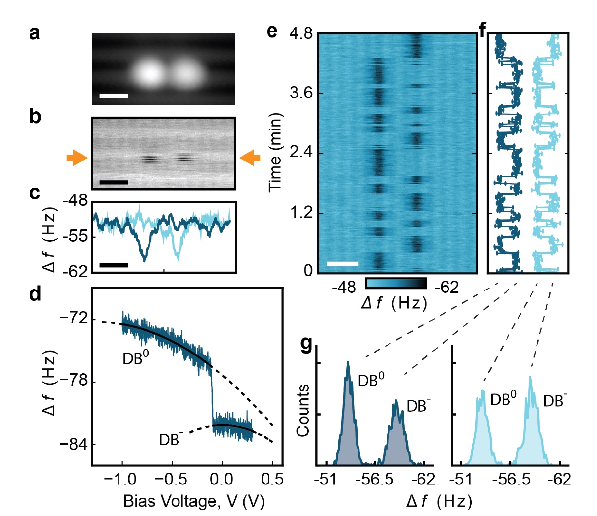
Image number 1
In image 1a, we see 2 NS structured by two intermediate hydrogen atoms using voltage pulses on the probe. This pair of NS contains 1 negative charge.
The image of a constant frequency shift (∆f) seems slightly shaded ( 1b ). This is due to the fact that the negative charge several times changed position in the process of obtaining this image. To be precise, they would have been jumped, as it were, from one NA to another, one hundred visible when scanning the structure of the sample ( 1c ).
Next, the researchers needed to determine that the change in contrast on ∆f images directly depends on the state of charge. For this, it was necessary to analyze an isolated HC, outside the pair, by conducting ∆f spectroscopy, which is dependent on displacement. The NS in the process of spectroscopy was negatively charged at 0 V on the sample with n-dopand ( 1d ). Here we see a very sharp transition between two parabolas, which corresponds to the transition from a neutral to a distinctive charge state of an individual NS.
In the image of 1f, we see how the charge changed position within 4.8 minutes. An important observation is that a negative charge can persist in the system for several seconds.
Researchers note a curious feature - negatively charged silicon NSAs stabilize at 200 meV (millielectronvolt). This is a consequence of lattice relaxation when the position of the nucleus of an atom rises above 30 pm relative to the neutral state. This prevents tunneling between HC-s.

Image number 2
It was also found that the HC state at 0 V strongly depends on ∆z. Confirmation of this statement was obtained by a series of scans using the method of constant height of the structure of six NS.

Comparison of the method of constant height (a) and constant tunneling current (b).
In the top shot 2b, it can be seen that, as the needle approaches the sample as close as possible (-320 pm), all six NS have a negative charge. If the needle is raised only by 50 pm to the level of -270 pm, then already 3 NS will be negatively charged (bottom shot 2b ). But the 2c graph shows that this change does not occur smoothly and linearly, on the contrary, there is a strong gap between -300 and -290 pm.
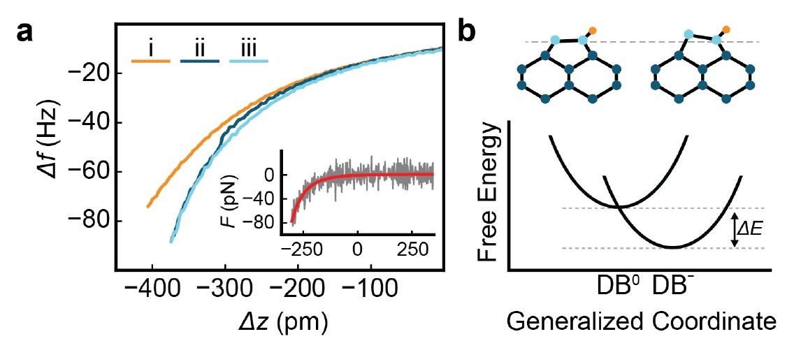
Image number 3
Observation of one abrupt transition, depending on the height of the needle, is not enough to make a full conclusion. Therefore, force spectroscopy was carried out at 0 V on individual NS in a pair (blue line at 3a ) and above the surface vacancy (orange line at 3a ). Initially, the distance between the sample and the needle was 700 pm larger than the reference height. Thus, all forces between the needle and the sample surface were leveled. Until the moment when ∆z = −100 pm, all three NS are almost identical, which confirms the predominance of long-range forces. A sharp increase in | ∆f | occurs when ∆z is reached at approximately -302 pm.
This leads to a hysteresis between the approximation curve and the drain curve, with | ∆f | remains high enough until ∆z reaches −100 pm. Scientists attribute this phenomenon to the localization of a pair of charge in the NA just below the needle.
For a more detailed study of the modes of reading and writing, several experiments were conducted with symmetric and asymmetric structures (out of 5 NN).
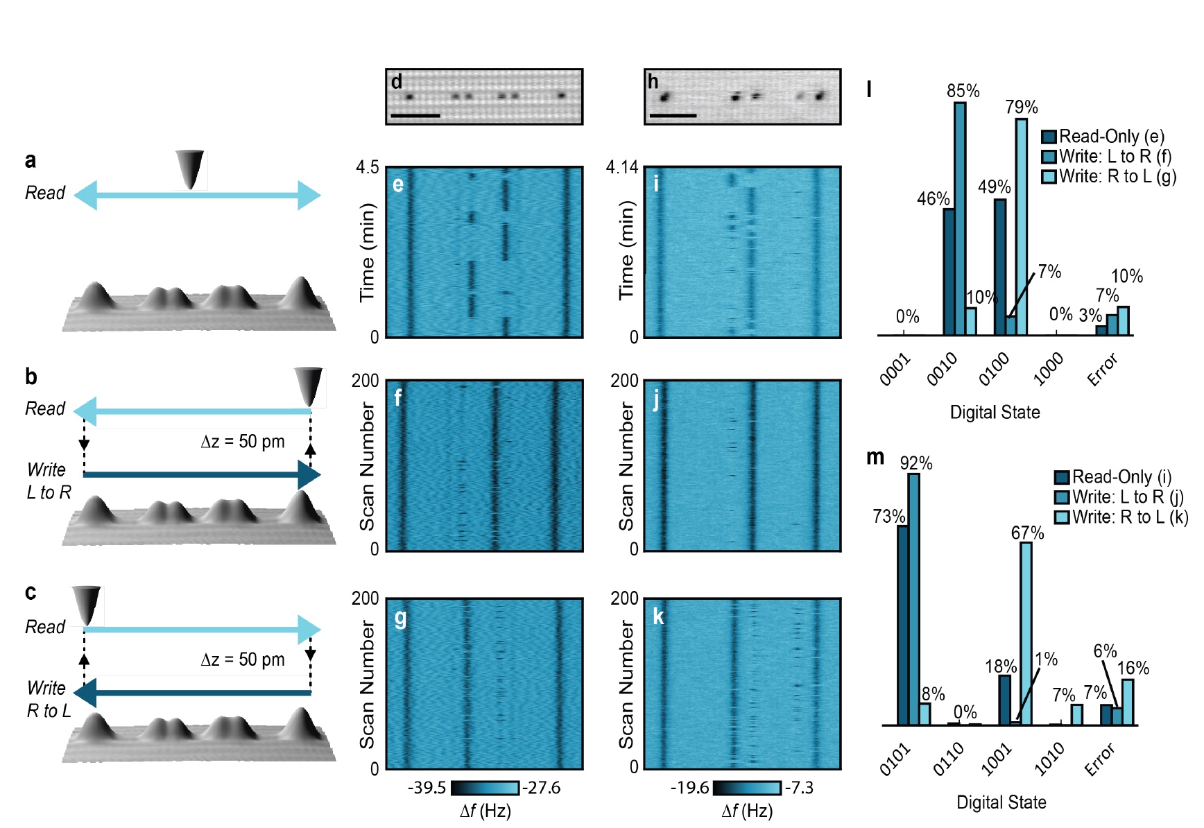
Image number 4
Figures 4a-c show the experimental designs of a symmetric ( 4d ) and asymmetric ( 4h ) structure.
During the recording mode, the needle passes above the figurative at a small distance, and in the reading mode, the needle moves back 50 m and continues to move in the opposite direction. Pairs of 4f / 4g and 4j / 4k images clearly show that the charge inside the structure can be fully manipulated in both structures.
In the case of a symmetrical structure, it was possible to shift the charge into one of the internal pair NAs: the right (image 4f ) and left ( 4g ). This was followed by a process of degeneration, the result of which is shown in image 4e.
In the case of an asymmetric structure, when the NA was only 5, three of them had a negative charge. Here we also managed to achieve charge manipulation in the internal pair of the National Assembly. But, given the asymmetry of the structure, both charge states did not degenerate.
For detailed information and research and additional materials to it I recommend reading the report of the researchers .
Epilogue
Scientists say that the above experimental results confirm the real possibility of manipulating electrons inside structures based on unsaturated bonds. The resulting charge state remains stable for several seconds, which is achieved by relaxing the silicon lattice, which stabilizes the negatively charged unsaturated bonds. In this case, the main tool in this experiment is the probe, and the process itself is completely independent of the bias voltage.
This study once again confirms that there is nothing impossible for scientists. Even the smallest objects are no longer available for study, and now for manipulation. Quantum computing and artificial neural networks may receive an additional impetus to development if this research continues. Let's hope that its potential is still as great as its authors want.
And a little humorous offtop :)
Thank you for staying with us. Do you like our articles? Want to see more interesting materials? Support us by placing an order or recommending to friends, 30% discount for Habr users on a unique analogue of the entry-level servers that we invented for you: The whole truth about VPS (KVM) E5-2650 v4 (6 Cores) 10GB DDR4 240GB SSD 1Gbps from $ 20 or how to share the server? (Options are available with RAID1 and RAID10, up to 24 cores and up to 40GB DDR4).
VPS (KVM) E5-2650 v4 (6 Cores) 10GB DDR4 240GB SSD 1Gbps until December for free if you pay for a period of six months, you can order here .
Dell R730xd 2 times cheaper? Only we have 2 x Intel Dodeca-Core Xeon E5-2650v4 128GB DDR4 6x480GB SSD 1Gbps 100 TV from $ 249 in the Netherlands and the USA! Read about How to build an infrastructure building. class c using servers Dell R730xd E5-2650 v4 worth 9000 euros for a penny?
Source: https://habr.com/ru/post/427009/
All Articles