Altium Designer: what to do if the project has become difficult?
Greetings I think any engineer or just a radio amateur / DIY engineer / maker engaged in the development of electronics, trying to develop their skills that grow with the complexity of the projects. At some point, a person reaches a level when it seems to him that projects have become very complex, will take a lot of time to develop and you need to do something about it - you need to optimize your work. Today I will tell how in Altium Designer 18 (hereinafter AD or AD18) to increase the productivity of their intellectual work and save time, nerves and money.
Now there is some information for those who do not know what Altium Designer is. This is one of three popular professional CAD systems that allow you to develop electronics of almost any complexity. The two remaining packages are Mentor Expedition (and PADS probably) and Allegro Cadence. Each of these 3 packages has its pros and cons, as well as conditional specialization. There will be no comparisons today, so I’ll just say why I chose Altium for myself:
Yes, yes, I did not talk about any simulation possibilities, tools, etc., but this is not necessary. All 3 of the above described CAD systems are technically able to do the same thing, simply with varying degrees of convenience and croncy.
')
Once, the year since 2011-2012, I had the opportunity to work for the first time in AD, it seemed to me cool, but scary, because at that moment, English was an obstacle for me and it was not at all clear how to work in it. The videos from comrade helped me to overcome my fear of a huge amount of tools and functionality. Sabunina (thanks to him), which are on youtube in Russian and describe the basic simple things that allowed us to take the first steps in mastering. Over the past 6 years, information on AD in Russian has become even more, so the threshold of entry has become even lower, so do not be afraid and learn.
To make it easier for you to master Altium Designer, I propose a couple of “gingerbreads” from you:
If in the process of studying you have any questions and have any difficulties, you can write me in private messages, if possible I try to answer everyone.
Any less serious project, be it the source code of a program or a circuit diagram of an electronic device, always has a trait after which chaos sets in, the project becomes incomprehensible, it is difficult to check and test it, it goes out of control.
This boundary is individual for each developer: one can perfectly understand the device of 1000 components, and the other begins to make mistakes and has difficulty with a project of 200 components. In general, the assessment in the number of electronic components is a bit subjective, but it allows to understand the general essence of the problem.
From the above written we can draw the following conclusion:
Until a certain moment, you can of course score on everything and “draw” anything and anything on the scheme, for example, like this:
Everything merges, the circuit is made carelessly and in the end it will lead to the fact that somewhere a crooked or wrong track was made, in this chaos they were not immediately noticed and as a result you cut the conductors on the boards and solder the snot.
Let's look at another masterpiece - the arduino scheme, made in AD:
How do you? It hurts me now ... I look at R2 and R3, it seems clear that these are suspenders for I2C, but where is this I2C and near which connector should they be a mystery to me and then you have to look for a long and tedious time, what’s the scheme with a small number of components and simple, but already chaos.
Now, as an alternative - an example from your works (clickable):
Look at the scheme and I think you immediately understand at least where the entrance is, and where the exit is, the “arrows” hint at it, and we are not Arabs, we read (including diagrams) from left to right. The module has one function - a three-phase common-mode filter and nothing superfluous. The scheme is done carefully and take 1 sheet in the documentation. 1 sheet - 1 function.
In fact, what I wrote above is small things that are important and make life easier, but still small things. Although I hope you caught the general ideology, let's summarize now how to “do”:
Now, having criticized others, it is necessary to propose an alternative “how to do”. It should be understood that the article describes only the subjective opinion of the author, based on work experience and own world view.
I propose to do like all normal people, that is, first we will makea bad version of the scheme through the ass , and then we will heroically solve all the problems and bring it to an acceptable state. Go!
Create a project in Altium Designer. In it, for example, I will depict a 6-phase buck DC / DC converter. I will have 6 power channels and 1 MK to control all phases. Each force channel will look as follows (clickable):

The channel itself power I originally drew correctly. If you look carefully, then I have signal inputs on the circuit - 2 PWMs on the left + VCCIN with GND, there is an output - VCC5V and GND. The module itself performs one task — converts VCCIN to 5V. We continue to do bad ...
Here we come across the first constraint - one channel occupies almost the entire sheet of A3, we have 6 of them, therefore if I increase the sheet to A2, it still does not fit. You can enlarge the list to A1 - fine, for now weare inexperienced developers and we follow this path and observe the following picture (clickable):
It seems so far understandable - there are 6 some pieces of the scheme, there is MK below. That's just 30% of the scheme, what else do you need? Binding MK + feedbacks? Of course! Does the device have to communicate with the outside world? Of course, add RS485. Aaaa, you still need power for drivers, that is, you need to get + 12V from VCCIN and add DC / DC for this! But MK ... he needs 1 more DC / DC and now adding all this - we look (clickable):
It is clear that here? And if I had not said originally about the functionality of the device? And if, in addition to this, even the individual pieces of the scheme were drawn clumsily? And if HBO components in libraries are drawn initially crooked? Scared? That's the same ...
Now let's think ... In this device, there are 150 components in all, in my medium projects connected with power electronics, they are usually from 1,500 to 4,000, that is, the scale of the disaster you can imagine when such A1 sheets will be 10 pieces higher and all of them are cluttered and crammed. Mistakes are inevitable!
We look and think further. The first thing to do is to create modules. I have them all formed, because I just copied them from one home craft, but one module crashed - the EEPROM memory for I2C is working. I made a mistake the same as in the arduin scheme, as it should be done:
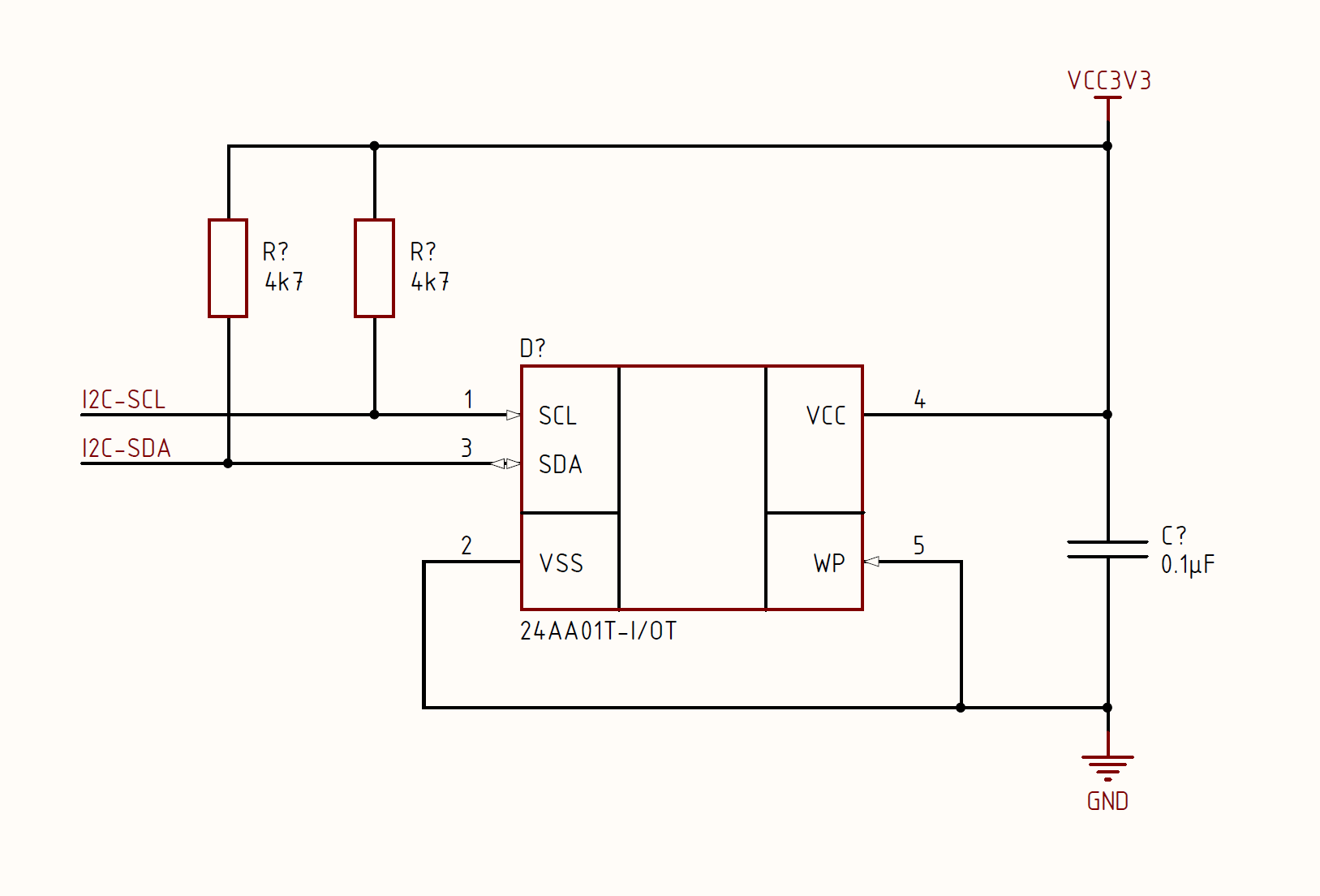
As you can see, I put together in one “handful” a memory chip, blocking a power capacitor, which will stand near it and pull up to + 3.3V. Now I don’t have to look for all the components that are needed for strapping the memory chip; they are all in one place. By the way, it is not necessary to allocate a separate sheet for each small microcircuit, yet the EEPROM is not a separate module, but rather a part of the microcontroller strapping. MK with strapping - this is a module worthy of a separate sheet.
Go ahead ... We have repeating parts of the circuit, for example, 2 absolutely identical channels for feedback on an operational amplifier (OU), another 6 absolutely identical power channels. This can be optimized too.
Another bright thought - if all the 6 channels of the buck are the same, then they will most likely have the same trace. This must take advantage. Maybe you can separate the roads for one module, and then the remaining 5 say "well, repeat"? It turns out you can, AD allows us to greatly facilitate our lives.
What is the beginning of any electronic device? From the idea of course. How to turn this idea into something material? For example, you can draw a flowchart where the macro functionality will be displayed. It is not necessary to be very wise, just a picture on a blackboard or a piece of paper:
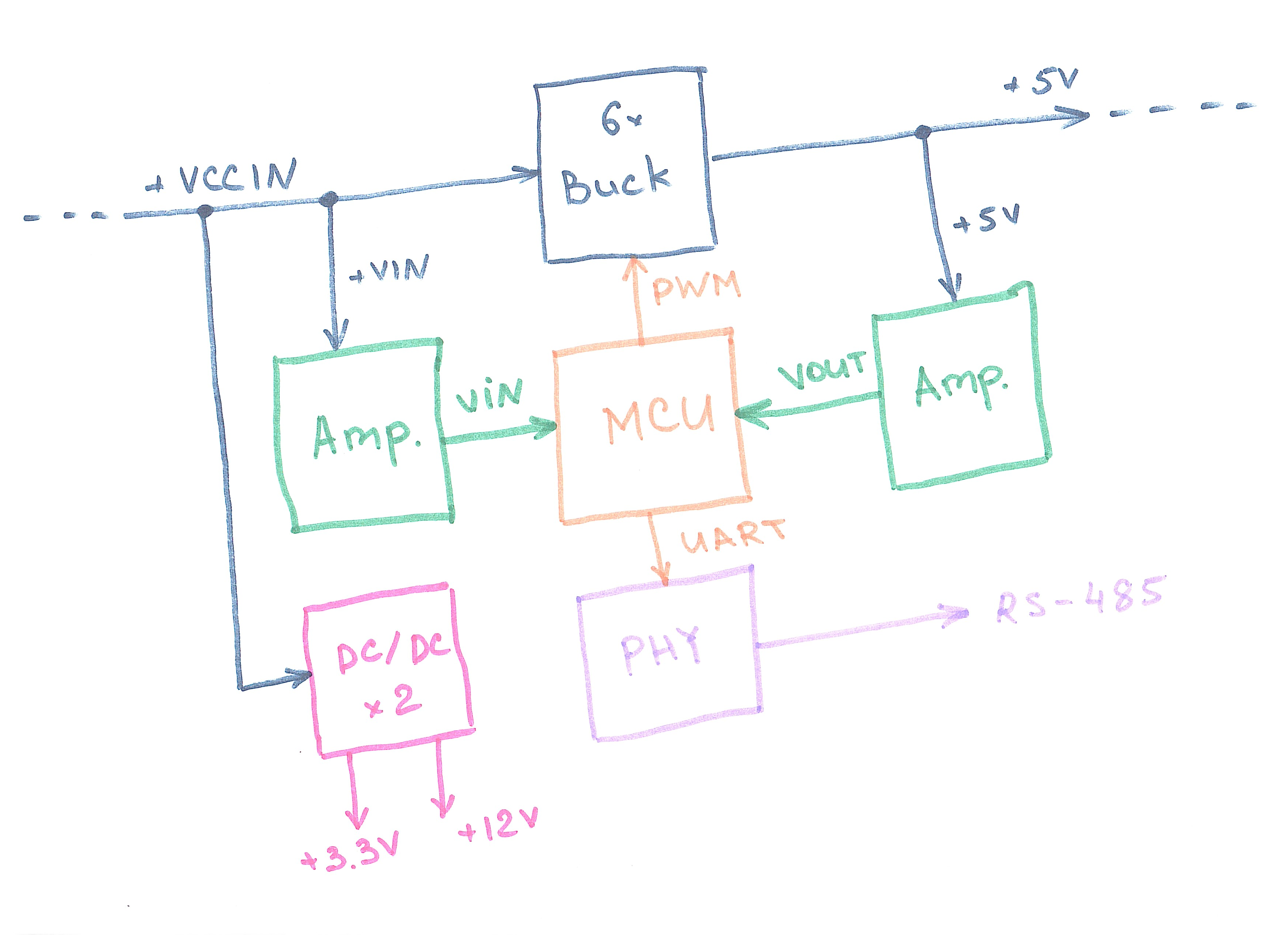
On the sheet fit all the functionality of our device. Firstly, this scheme lets us understand how the device basically works: there is a power part (Buck) 6-channel, which is controlled by a MC (MCU), which for control produces 2 feedback signals through an op-amp (Amp.), And there is also a pair of dc / dc for power supply and a Modbus interface for communication with the world. Secondly, the scheme immediately shows ready-made functional blocks.
Now we need to create 5 sheets of A3 in AD and transfer the corresponding part of the scheme to each, but before that we need to consider the types of connections and circuits that we will use in AD:
Now we need to set the signals that will go beyond the limits of the module using Place Port. For example, for a module with an operational amplifier, it would look like this:
Now our module has turned into a completely logical part of the circuit: it has an input (INPUT), there is an output (ADC-OUT) and there are 2 global connections (Power Port) - GND and VCC3V3. Nothing extra. Do the same for other modules and do automatic assignment of numbers to symbols (designator) by going to Tools -> Annotations -> Annotate Schematics and clicking Update Changes List :
Next, click Accept Changes and in the window that opens, click Execute Changes :

We close the extra windows and see that our designations (D ?, R?, C? Etc.) have received unique numbers. After the done actions, we get the following project - PDF .
Well, how? I think no one will argue - everything is neat, it is clear how it works at first glance, there is no garbage dump on the diagram. Now it remains for the small - somehow we need to create 6 channels from one sheet and, in general, put everything together in a heap.
To do this, create a new sheet, I will have it just called Main design , but the name can be any. In this sheet we will have a block diagram, which I previously painted by hand. To create a module go Place -> Sheet Symbol . Now we will give our element the style of the entire project, that is, the font (I have ISOCPEUR), the width and color of the frame, the designator and so on, and also write the name of the sheet with our module:
Now right-click on our module (orange square) and go to Sheet Symbol Actions -> Synchronize Sheet Entries and Port and the window will open:
In it we see a list of our Place Port. We select everything and click Add Sheet Entries , install it in our module and set the general font type, we get this module:

Now we repeat the same for the remaining 4 modules and at the output we get the following structure:
Here you should pay attention to 2 points:
Now that we have created all the modules, we need to increase their number in order to get 6 channels for the power section and 2 channels for operational amplifiers. As they say, there are always two ways out, even if you have been eaten, and this case is no exception. I will show both ways:
With this we will finish with the concept, the final result here is PDF . As you can see the scheme came out the simplest, just a couple of semi-empty sheets of A3, any radio amateur with minimal time and nerves can understand it.
In modern realities, when the degree of integration of components (chips) is quite high, the development of the concept takes less and less time. Already not so often you will meet on 90% of analog monsters and it is good. "Weakness" in the development process of the device is the design of the printed circuit board (PCB). Modern CAD systems provide many different tools to reduce labor costs for the development of the board, and this was the main purpose of this article.
As I indicated earlier, there are several duplicate modules in our device: buck and OU. If you look at modern devices, many will have many such repetitions, for example, a 4-channel oscilloscope in which all channels are identical. Of course, we can trace each channel with our hands, and we can simplify our life.
Everything that was previously described in the article is simply called a multi-channel scheme , it sounds simple and tasteful. We have created such a schematic diagram and now it will allow us to do the following - to separate the chains for one channel buck, and then simply copy the components and the layout (layout) and all conductors to the remaining 5. To begin with, we transfer all our components from a schematic diagram to a file with a printed circuit board, click Design -> Update PCB Document :
Now click Execute Changes and as a result we get the following PCB:

As you can see on the board appeared 6 red zones, which are called rooms (Room). In each room are electronic components for one channel and nothing more. Now you need to set the dimensions of the room, that is, specify what specific area will occupy the components of our channel and make the layout of parts. It looks like this:
So the components of each channel will be located and that is exactly the area to occupy. True, something I do not like here ... Aha! The designations of the components in the silk-screen layer (white lettering) are not continuous numbering, but the numbering in the “Designation_ Room Name” format, that is, we have R6_BUCK1, R6_BUCK2 resistors and so on. I want to avoid the prefix "_BUCK1" and each component had its own number. Press Ctrl + L and then go to the Annotate Options menu, where we see this menu:
Now you need to choose the numbering option $ ComponentPrefix $ GlobalIndex and click OK. Click Reset All to drop all values and then click Anotate Designated . As we see in the channel BUCK2, the components changed their designations from R6_BUCK2 to the more familiar designations R6, R7, etc .:

It remains to agree with the changes by clicking Accept Changes and in the window that opens confirm all by clicking on Execute Changes . We transfer the changes from the scheme to the PCB Design -> Update PCB Documet as we have already done. As a result, we observe “human” designations that do not occupy the entire charge and spoil it:
Having an adequate layout and designations go to the trace - let's trace the chains inside one room of “BUCK6” and get just such a picture:
I did not plant everything, GND left untouched, because This is usually a single polygon filled. Enough to demonstrate. Now do the following:
I didn’t check and chose 2 channels with clicks, since There are situations when, for example, not all channels are identical. Remember the VRM on the motherboard of the CPU, there are often 3-4 phases on the one hand, and 3-4 more on the other. In my case, these can be 3 phases with one wiring and 3 more phases with another. I think the general ideology is clear. Now let's look at the result:

We observe 3 identical channels and most importantly - time I spent on all channels as 1. In this abstract case, the time saving is 6 times, but in real tasks the order of reducing labor costs is about the same. Yes, and not unimportant factor - if you make 6 channels with your hands, then the "eye is washed out" because of the same type of work and it is likely to make a mistake or make a curve layout.
I hope you were interested to learn about one of the basic design paradigms of electronics and get something new and useful for yourself. And remember - accuracy in the documentation, libraries and the use of the right tools in CAD will allow you to avoid mistakes and save a lot of time.
Introduction
Now there is some information for those who do not know what Altium Designer is. This is one of three popular professional CAD systems that allow you to develop electronics of almost any complexity. The two remaining packages are Mentor Expedition (and PADS probably) and Allegro Cadence. Each of these 3 packages has its pros and cons, as well as conditional specialization. There will be no comparisons today, so I’ll just say why I chose Altium for myself:
- Excellent design and thoughtful interface of this program is simply out of competition. Just look at the competitors and everything becomes clear. Yes, design and convenience are important when you spend several hours a day at work. It also facilitates the process of learning newbies, because learning in a clear and logical CAD system is much easier;
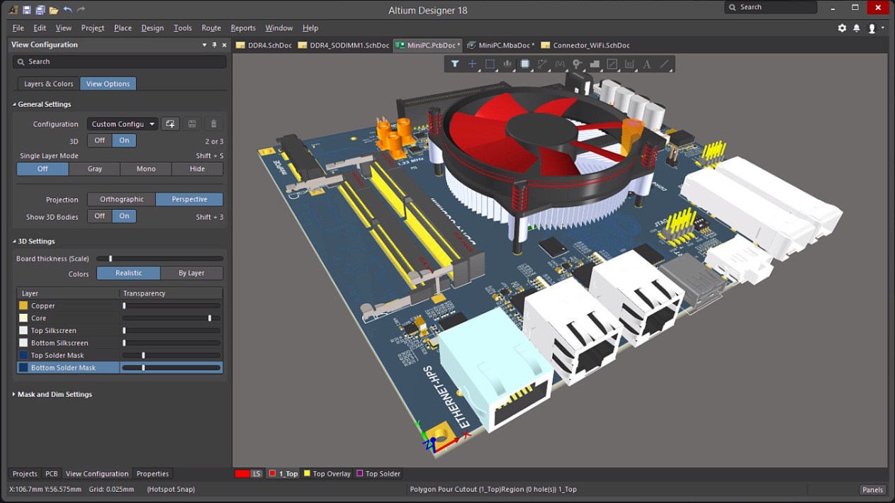
- The ability to work directly with such a mechanical "titanium" as SolidWorks. We can simply open the board from AD in solid view and add it as part of the assembly without losing quality. Goodbye STEP conversion. For me, and certainly for you, this is important, because An electronic device is not just a board with components, it is almost always the case. This feature allows you to easily make an assembly model of the entire device and prevent errors in the design and manufacture of molds of 3-5 thousand $ each;
- The presence of a sufficiently large amount of information in Russian, which provides a fairly low threshold of entry. This is the main reason why Altium dominates the CIS, and not something else. Try to find something in Russian by Mentor or Cadence, immediately want to learn to work in them;
- In the CIS and Asia, most companies operate in Altium, and in the States they have a large market share. In Europe, they love SolidWorks PCB, which is just the built-in AD. What does this give? You can easily find a job if you decide to work in the field of electronics development.
Yes, yes, I did not talk about any simulation possibilities, tools, etc., but this is not necessary. All 3 of the above described CAD systems are technically able to do the same thing, simply with varying degrees of convenience and croncy.
')
I want to learn how to work in Altium, but it scares me
Once, the year since 2011-2012, I had the opportunity to work for the first time in AD, it seemed to me cool, but scary, because at that moment, English was an obstacle for me and it was not at all clear how to work in it. The videos from comrade helped me to overcome my fear of a huge amount of tools and functionality. Sabunina (thanks to him), which are on youtube in Russian and describe the basic simple things that allowed us to take the first steps in mastering. Over the past 6 years, information on AD in Russian has become even more, so the threshold of entry has become even lower, so do not be afraid and learn.
To make it easier for you to master Altium Designer, I propose a couple of “gingerbreads” from you:
- The cycle of educational video lessons is here . The clips have a long duration, but contain comprehensive information on the basic function (as they say at least) and will allow any schoolchild to design their first device without problems;
- Libraries for Altium Designer - here . Here you will find all the passive components (resistors, capacitors, etc.), as well as a large number of popular transistors, diodes and chips, including MK and FPGA. Creating libraries at the start takes a lot of time, so I hope that I will save you a lot of time.
If in the process of studying you have any questions and have any difficulties, you can write me in private messages, if possible I try to answer everyone.
When does a project get complicated?
Any less serious project, be it the source code of a program or a circuit diagram of an electronic device, always has a trait after which chaos sets in, the project becomes incomprehensible, it is difficult to check and test it, it goes out of control.
This boundary is individual for each developer: one can perfectly understand the device of 1000 components, and the other begins to make mistakes and has difficulty with a project of 200 components. In general, the assessment in the number of electronic components is a bit subjective, but it allows to understand the general essence of the problem.
From the above written we can draw the following conclusion:
The project becomes difficult when the developer becomes necessary to perform actions to preserve the readability and clarity of the source code of the project.
Until a certain moment, you can of course score on everything and “draw” anything and anything on the scheme, for example, like this:
Everything merges, the circuit is made carelessly and in the end it will lead to the fact that somewhere a crooked or wrong track was made, in this chaos they were not immediately noticed and as a result you cut the conductors on the boards and solder the snot.
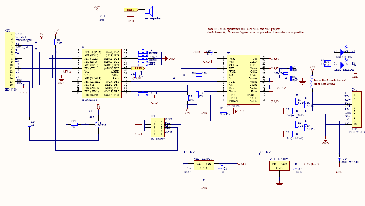
Let's look at another masterpiece - the arduino scheme, made in AD:
How do you? It hurts me now ... I look at R2 and R3, it seems clear that these are suspenders for I2C, but where is this I2C and near which connector should they be a mystery to me and then you have to look for a long and tedious time, what’s the scheme with a small number of components and simple, but already chaos.
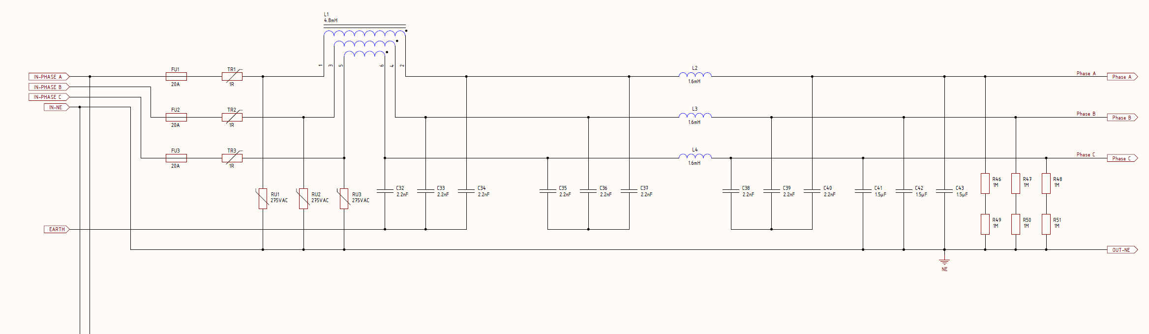
Now, as an alternative - an example from your works (clickable):
Look at the scheme and I think you immediately understand at least where the entrance is, and where the exit is, the “arrows” hint at it, and we are not Arabs, we read (including diagrams) from left to right. The module has one function - a three-phase common-mode filter and nothing superfluous. The scheme is done carefully and take 1 sheet in the documentation. 1 sheet - 1 function.
In fact, what I wrote above is small things that are important and make life easier, but still small things. Although I hope you caught the general ideology, let's summarize now how to “do”:
- The principle of encapsulation is also applicable in circuit design: each module performs a single simple task . A module is usually a single sheet in the documentation, for example, some A3;
- The schematic diagram should be performed in the same style and very carefully. Accuracy when working in the future will pay off in full. And when you show an understandable, carefully executed scheme about the interview, you will immediately have a good impression. They see hands at once and usually do not like them;
- Do not use sheets larger than A2, even if you have a couple thousand components. If you want to stick A1, then something you are doing wrong. Probably you need to select some modules on the scheme and transfer them to a separate sheet.
Criticize? Offer!
Now, having criticized others, it is necessary to propose an alternative “how to do”. It should be understood that the article describes only the subjective opinion of the author, based on work experience and own world view.
I propose to do like all normal people, that is, first we will make
Create a project in Altium Designer. In it, for example, I will depict a 6-phase buck DC / DC converter. I will have 6 power channels and 1 MK to control all phases. Each force channel will look as follows (clickable):
The channel itself power I originally drew correctly. If you look carefully, then I have signal inputs on the circuit - 2 PWMs on the left + VCCIN with GND, there is an output - VCC5V and GND. The module itself performs one task — converts VCCIN to 5V. We continue to do bad ...
Here we come across the first constraint - one channel occupies almost the entire sheet of A3, we have 6 of them, therefore if I increase the sheet to A2, it still does not fit. You can enlarge the list to A1 - fine, for now we
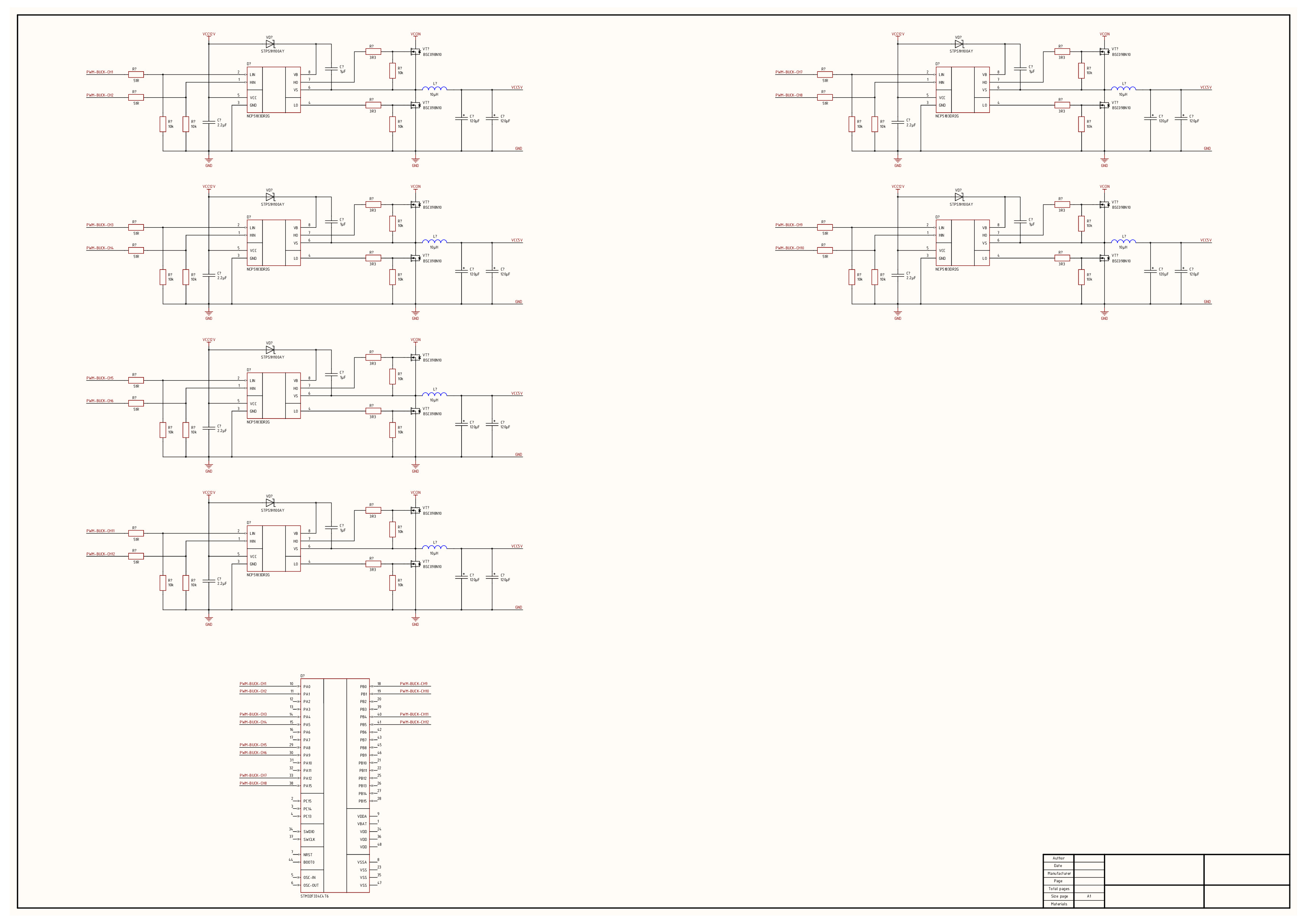
It seems so far understandable - there are 6 some pieces of the scheme, there is MK below. That's just 30% of the scheme, what else do you need? Binding MK + feedbacks? Of course! Does the device have to communicate with the outside world? Of course, add RS485. Aaaa, you still need power for drivers, that is, you need to get + 12V from VCCIN and add DC / DC for this! But MK ... he needs 1 more DC / DC and now adding all this - we look (clickable):
It is clear that here? And if I had not said originally about the functionality of the device? And if, in addition to this, even the individual pieces of the scheme were drawn clumsily? And if HBO components in libraries are drawn initially crooked? Scared? That's the same ...
What to do?
Now let's think ... In this device, there are 150 components in all, in my medium projects connected with power electronics, they are usually from 1,500 to 4,000, that is, the scale of the disaster you can imagine when such A1 sheets will be 10 pieces higher and all of them are cluttered and crammed. Mistakes are inevitable!
We look and think further. The first thing to do is to create modules. I have them all formed, because I just copied them from one home craft, but one module crashed - the EEPROM memory for I2C is working. I made a mistake the same as in the arduin scheme, as it should be done:
As you can see, I put together in one “handful” a memory chip, blocking a power capacitor, which will stand near it and pull up to + 3.3V. Now I don’t have to look for all the components that are needed for strapping the memory chip; they are all in one place. By the way, it is not necessary to allocate a separate sheet for each small microcircuit, yet the EEPROM is not a separate module, but rather a part of the microcontroller strapping. MK with strapping - this is a module worthy of a separate sheet.
Go ahead ... We have repeating parts of the circuit, for example, 2 absolutely identical channels for feedback on an operational amplifier (OU), another 6 absolutely identical power channels. This can be optimized too.
Another bright thought - if all the 6 channels of the buck are the same, then they will most likely have the same trace. This must take advantage. Maybe you can separate the roads for one module, and then the remaining 5 say "well, repeat"? It turns out you can, AD allows us to greatly facilitate our lives.
Let's do beautiful!
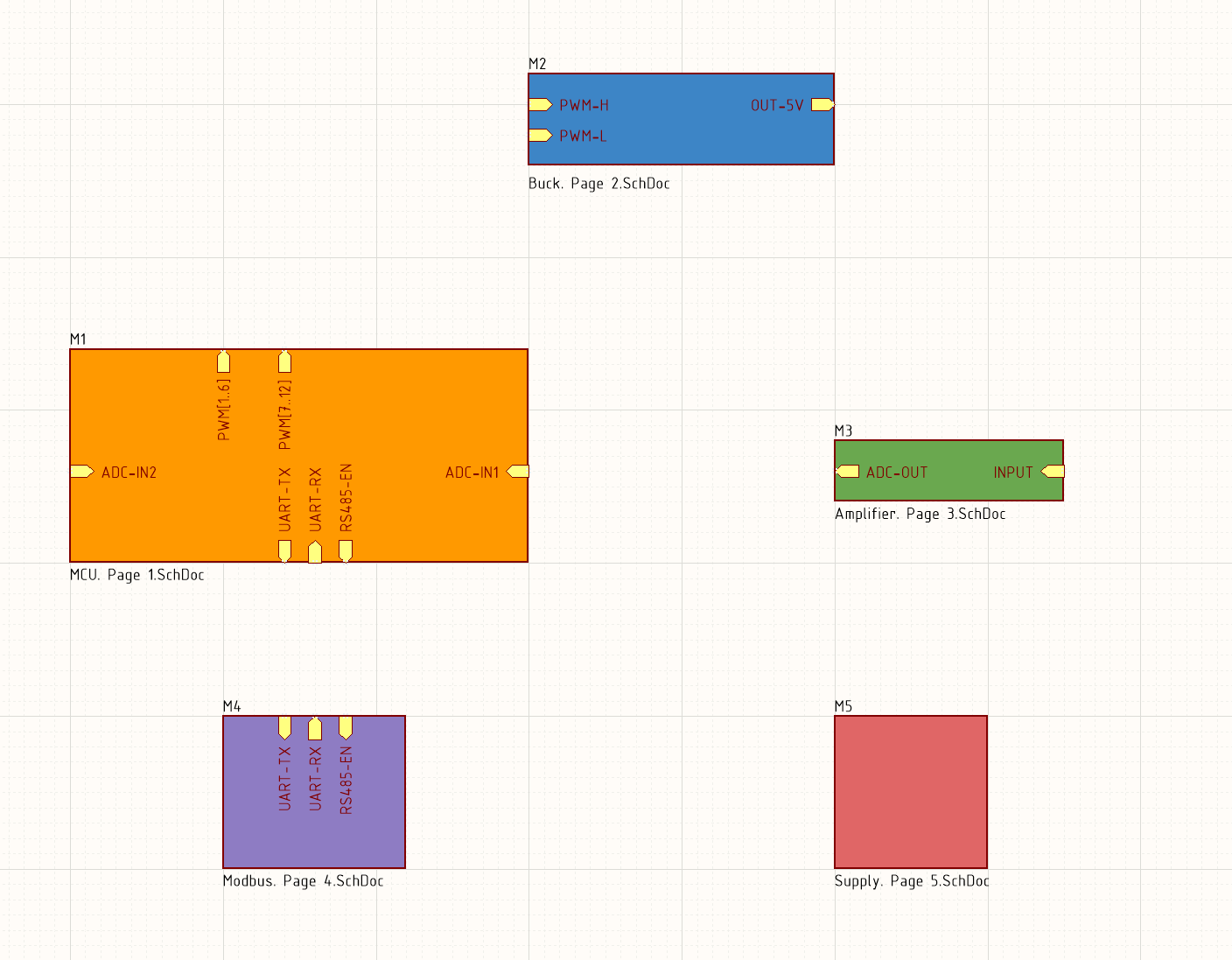
What is the beginning of any electronic device? From the idea of course. How to turn this idea into something material? For example, you can draw a flowchart where the macro functionality will be displayed. It is not necessary to be very wise, just a picture on a blackboard or a piece of paper:
On the sheet fit all the functionality of our device. Firstly, this scheme lets us understand how the device basically works: there is a power part (Buck) 6-channel, which is controlled by a MC (MCU), which for control produces 2 feedback signals through an op-amp (Amp.), And there is also a pair of dc / dc for power supply and a Modbus interface for communication with the world. Secondly, the scheme immediately shows ready-made functional blocks.
Now we need to create 5 sheets of A3 in AD and transfer the corresponding part of the scheme to each, but before that we need to consider the types of connections and circuits that we will use in AD:
- Power port
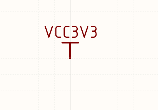
This type is global throughout the project. That is, if we put such a port on one sheet and on the other, they will unite into a single chain with the name "VCC3V3". Accordingly, in addition, the power supply on different sheets is not necessary to connect. This type of port only sets the power circuit and ground (GND); - Net lable
A tool for assigning the name of a specific circuit in the diagram. Chains with the same name (NetLabel) are combined both inside one sheet and outside. We will use this tool kosher, that is, only to specify names and connections within a single sheet; - Place Port

Tool for intermodular connections. In contrast to NetLabel, which serves to connect inside a module / sheet, this port is used to communicate with the “outside world”. To them we interconnect the modules, all circuits except power and ground (GND).
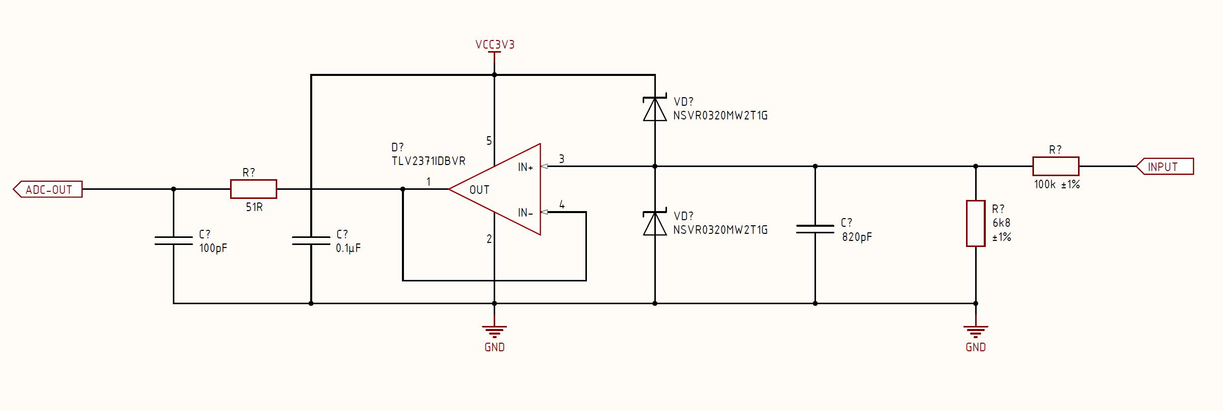
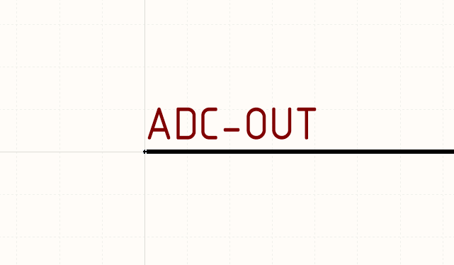
Now we need to set the signals that will go beyond the limits of the module using Place Port. For example, for a module with an operational amplifier, it would look like this:
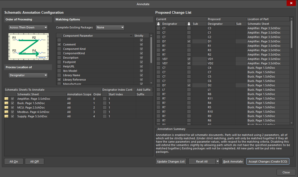
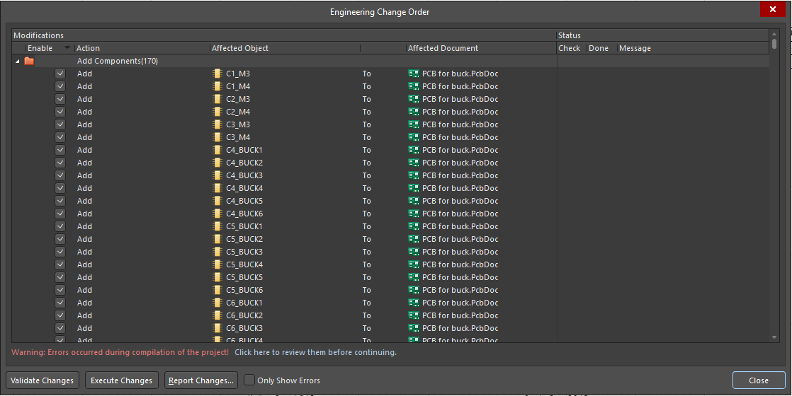
Now our module has turned into a completely logical part of the circuit: it has an input (INPUT), there is an output (ADC-OUT) and there are 2 global connections (Power Port) - GND and VCC3V3. Nothing extra. Do the same for other modules and do automatic assignment of numbers to symbols (designator) by going to Tools -> Annotations -> Annotate Schematics and clicking Update Changes List :
Next, click Accept Changes and in the window that opens, click Execute Changes :
We close the extra windows and see that our designations (D ?, R?, C? Etc.) have received unique numbers. After the done actions, we get the following project - PDF .
Well, how? I think no one will argue - everything is neat, it is clear how it works at first glance, there is no garbage dump on the diagram. Now it remains for the small - somehow we need to create 6 channels from one sheet and, in general, put everything together in a heap.
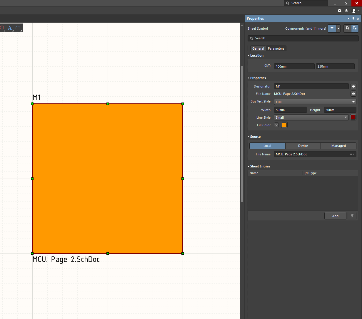
To do this, create a new sheet, I will have it just called Main design , but the name can be any. In this sheet we will have a block diagram, which I previously painted by hand. To create a module go Place -> Sheet Symbol . Now we will give our element the style of the entire project, that is, the font (I have ISOCPEUR), the width and color of the frame, the designator and so on, and also write the name of the sheet with our module:
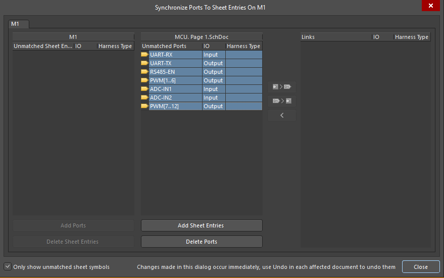
Now right-click on our module (orange square) and go to Sheet Symbol Actions -> Synchronize Sheet Entries and Port and the window will open:
In it we see a list of our Place Port. We select everything and click Add Sheet Entries , install it in our module and set the general font type, we get this module:
Now we repeat the same for the remaining 4 modules and at the output we get the following structure:
Here you should pay attention to 2 points:
- The 5th page (Page 5) with dc / dc will not detect the Place Port when trying to synchronize, and if you look at the module circuit, then they really are not there, only the Power Port. BUT! It is imperative to remove the module, otherwise the components from this sheet simply will not appear on the board;
- Note that the Place Port tool has a directivity parameter: input, output, and bidirectional. You should correctly determine the type of port for your signal, for example, the PWM-H ports are output for the MCU module and input for the Buck module.
Clone
Now that we have created all the modules, we need to increase their number in order to get 6 channels for the power section and 2 channels for operational amplifiers. As they say, there are always two ways out, even if you have been eaten, and this case is no exception. I will show both ways:
- Copy to hand-to-hand
Everything is simple - the usual copy-paste. Select our module, Ctrl + C and Ctrl + V - we get a new module. It remains only to change its designator number from M3 to M6. Then we connect everything and get an intermediate version of the scheme: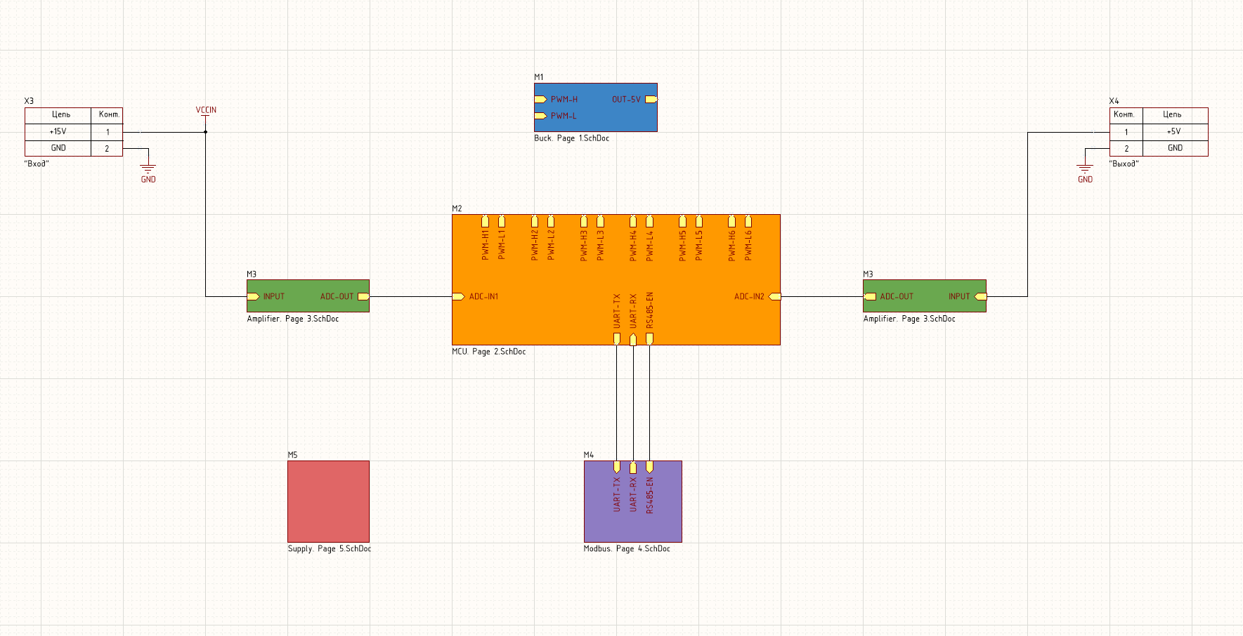
I copied the module OU, added a pair of connector and tires GND and VCCIN, they are now global and are connected at once in all modules where they occur. Drag it apart Place Port in this case makes no sense. I also connected all external circuits except the Buck module, I will demonstrate the 2nd, more compact, method on it. - Jedi Copy
In contrast to the previous version, everything is difficult to understand here, but it is easier to implement and, most importantly, more competently. Creation of several channels will be carried out using the REPEAT directive. To do this, instead of designation M1, we write the REPEAT command (BUCK, 1, 6) . This command will create channels with designations (designator) from BUCK1 to BUCK6, that is, our 6 pieces. Click Enter and see how AD has created the required number of channels: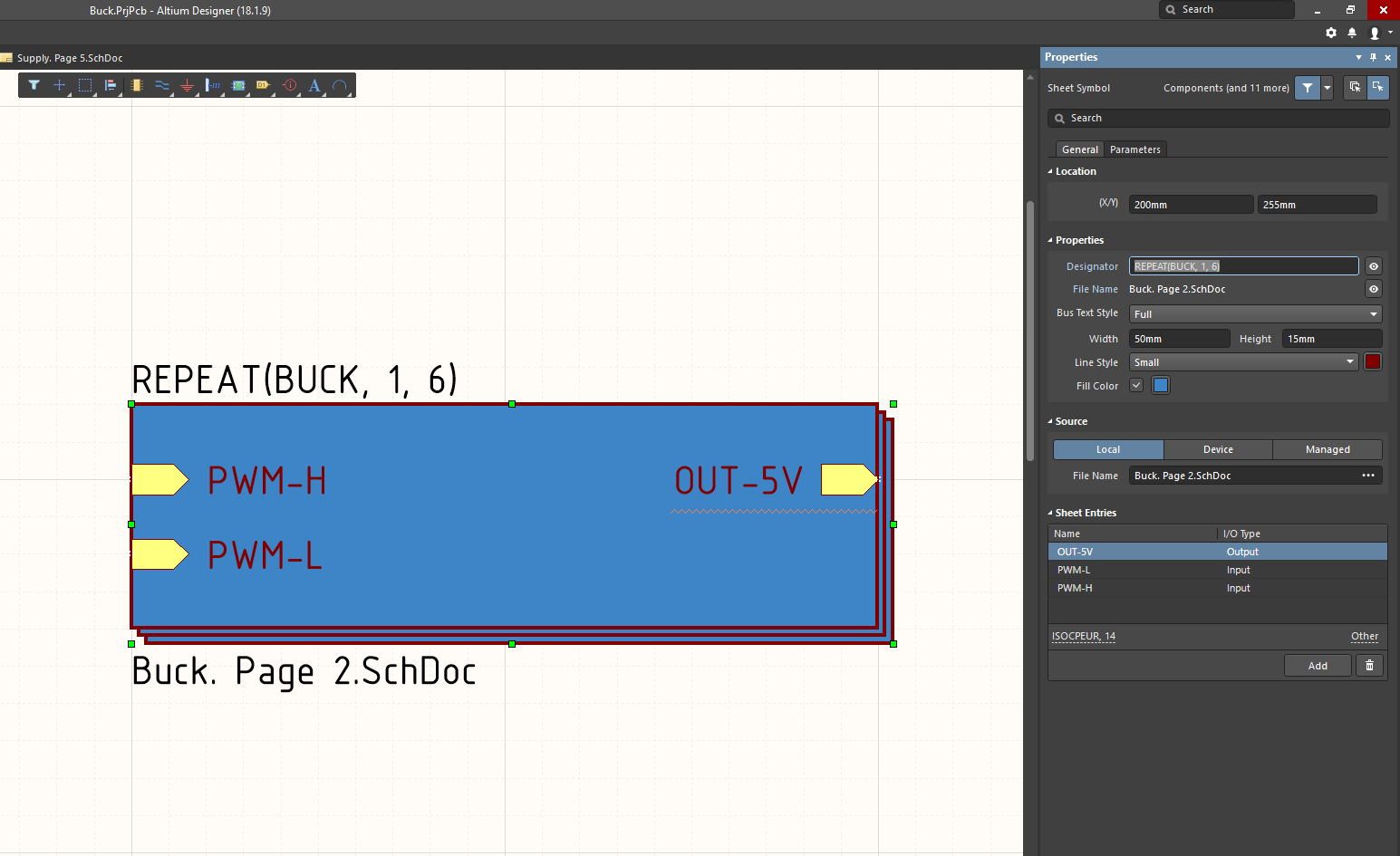
Now you need to connect the chain. I'll start with a simple one - our OUT-5V outputs on all channels should be combined, since All our phases work as one converter to a common output. To do this, we just from Place Port displays the usual circuit and connect it to the output connector: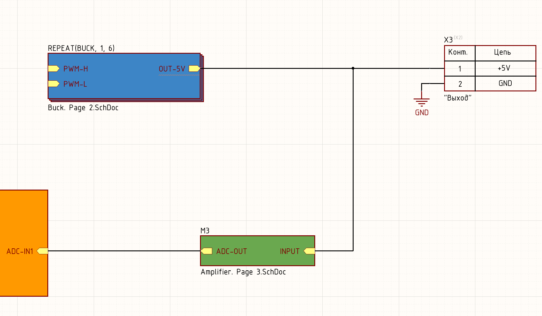
Now you need to tell AD that our PWM-H ports are not one port / circuit, but 6 separate channels. To do this, click on the Place Port with the name PWM-H and in the column with the name write REPEAT (PWM-H) , this will create 6 different chains: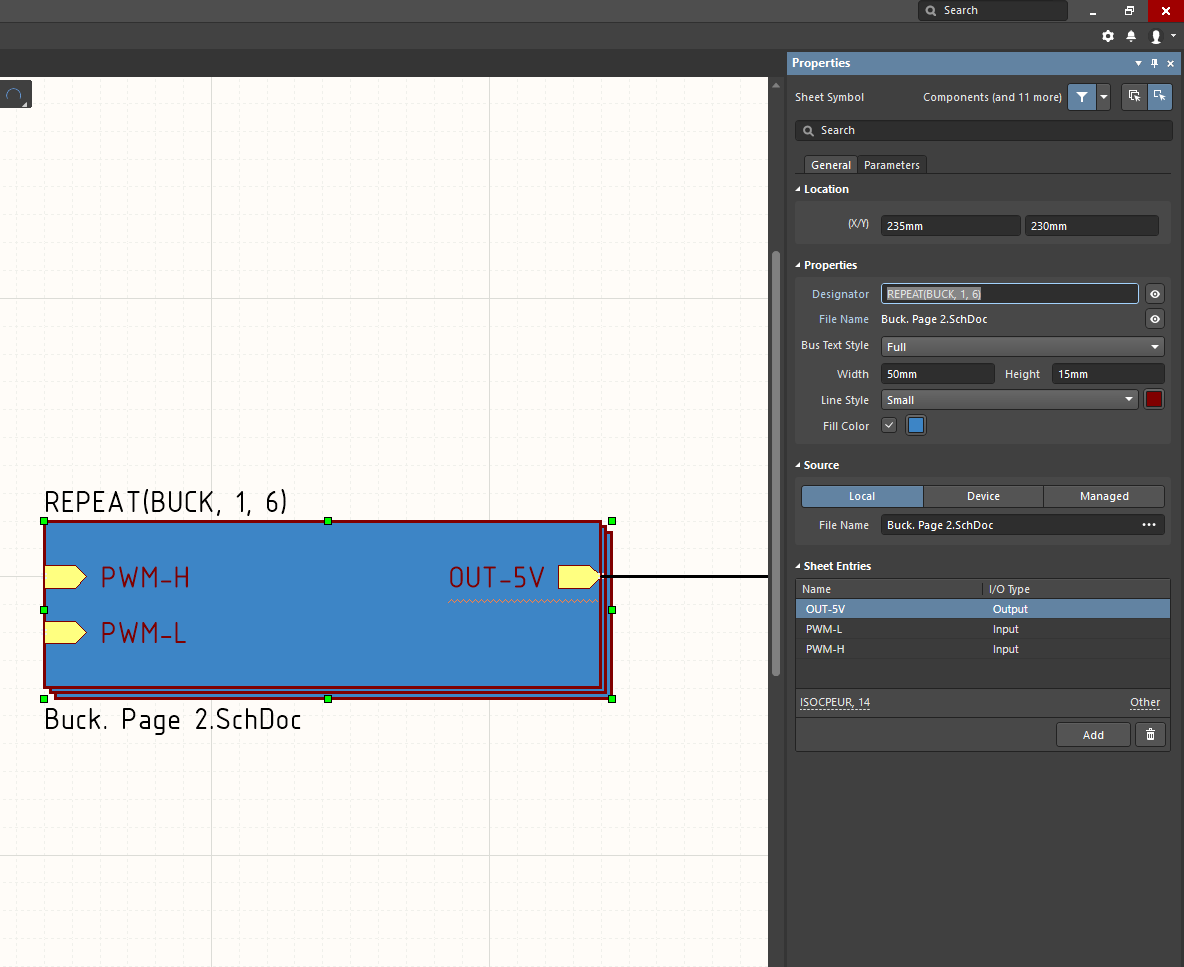
Now you need to bring the usual chain (Ctrl + W) from the Place Port named REPEAT (PWM-H) and give this chain the name PWM-H using the NetLabel tool. Then the bus must be removed from the circuit and given its name PWM-H [1..6] . Thus, from one port we brought out 6 different circuits which will have the names PWM-H1, PWM-H2 and so on: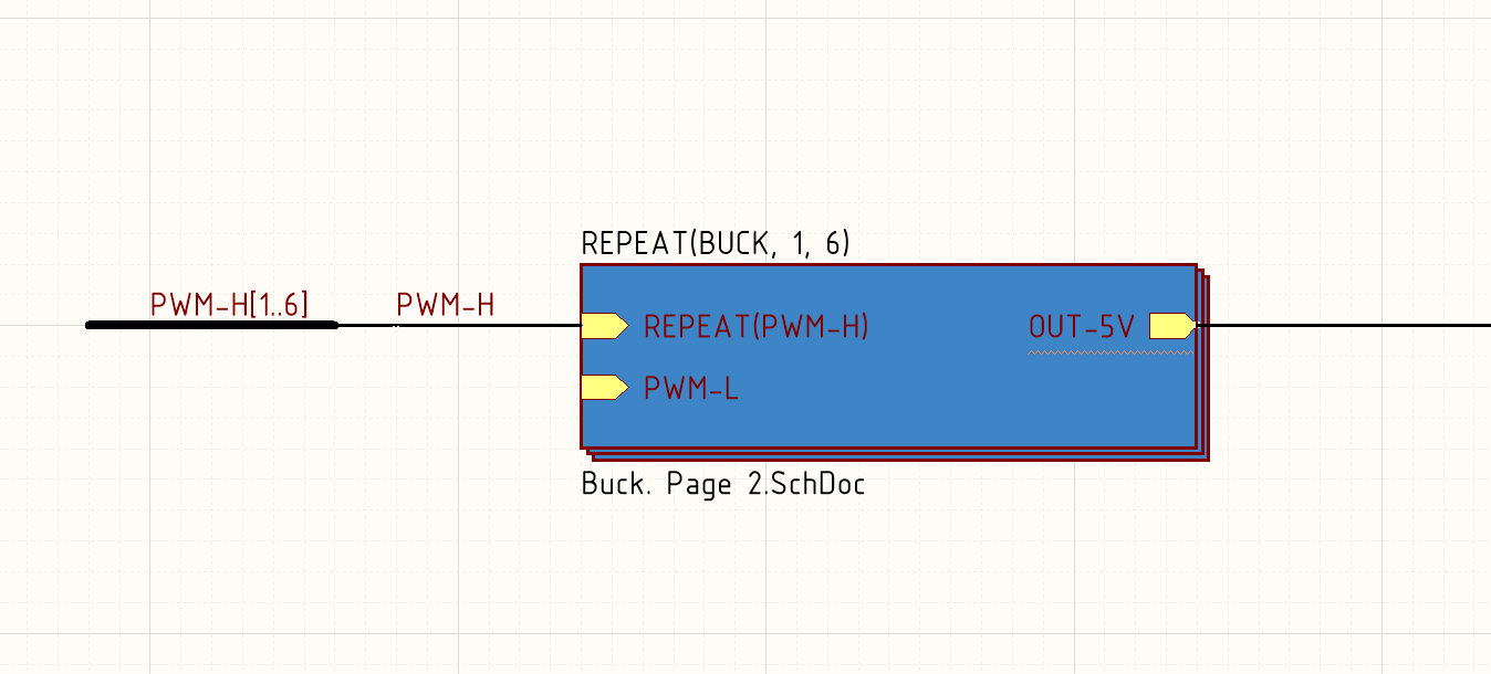
Next, we connect the PWM-H bus [1..6] to the bus output on the MCU module for the upper half-bridge transistors. Similar procedures also need to be carried out for the lower transistors and also bus bus, in the end we will have the following circuit: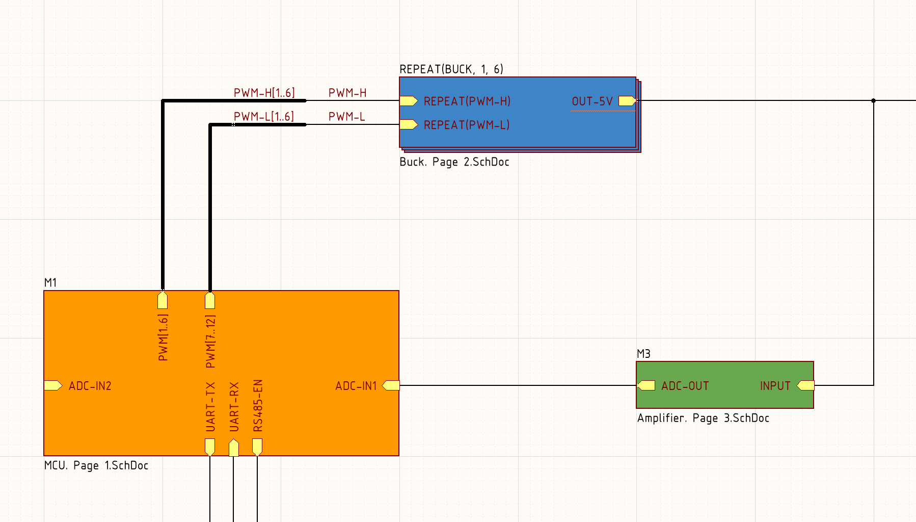
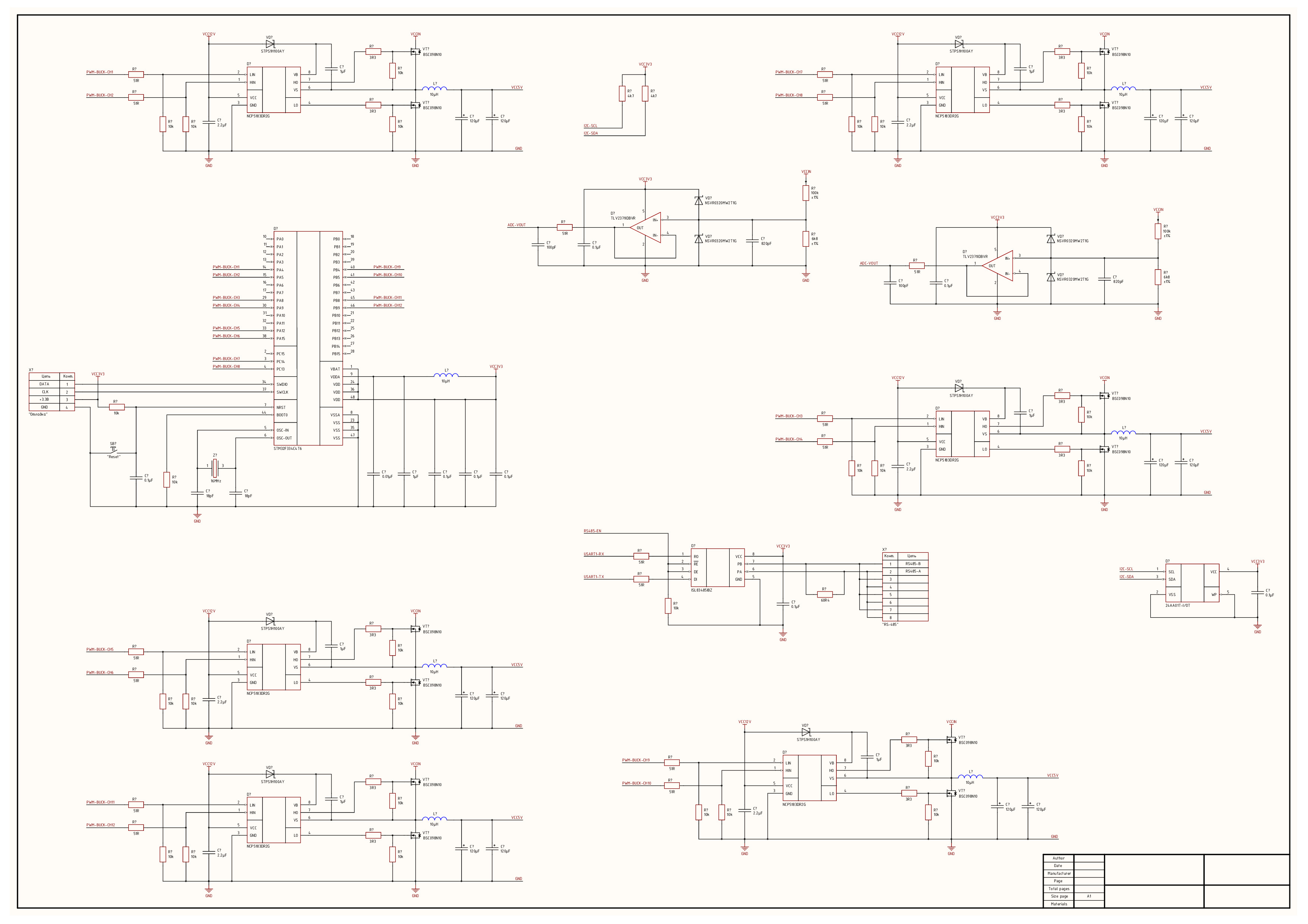
Now, having known Zen, let us redo the Jedi-like module with an operational amplifier in order not to leave a crutch in the form of copy-paste. As a result, we get the final version of the concept:
With this we will finish with the concept, the final result here is PDF . As you can see the scheme came out the simplest, just a couple of semi-empty sheets of A3, any radio amateur with minimal time and nerves can understand it.
Save dozens of man hours on the trace.
In modern realities, when the degree of integration of components (chips) is quite high, the development of the concept takes less and less time. Already not so often you will meet on 90% of analog monsters and it is good. "Weakness" in the development process of the device is the design of the printed circuit board (PCB). Modern CAD systems provide many different tools to reduce labor costs for the development of the board, and this was the main purpose of this article.
As I indicated earlier, there are several duplicate modules in our device: buck and OU. If you look at modern devices, many will have many such repetitions, for example, a 4-channel oscilloscope in which all channels are identical. Of course, we can trace each channel with our hands, and we can simplify our life.
Everything that was previously described in the article is simply called a multi-channel scheme , it sounds simple and tasteful. We have created such a schematic diagram and now it will allow us to do the following - to separate the chains for one channel buck, and then simply copy the components and the layout (layout) and all conductors to the remaining 5. To begin with, we transfer all our components from a schematic diagram to a file with a printed circuit board, click Design -> Update PCB Document :
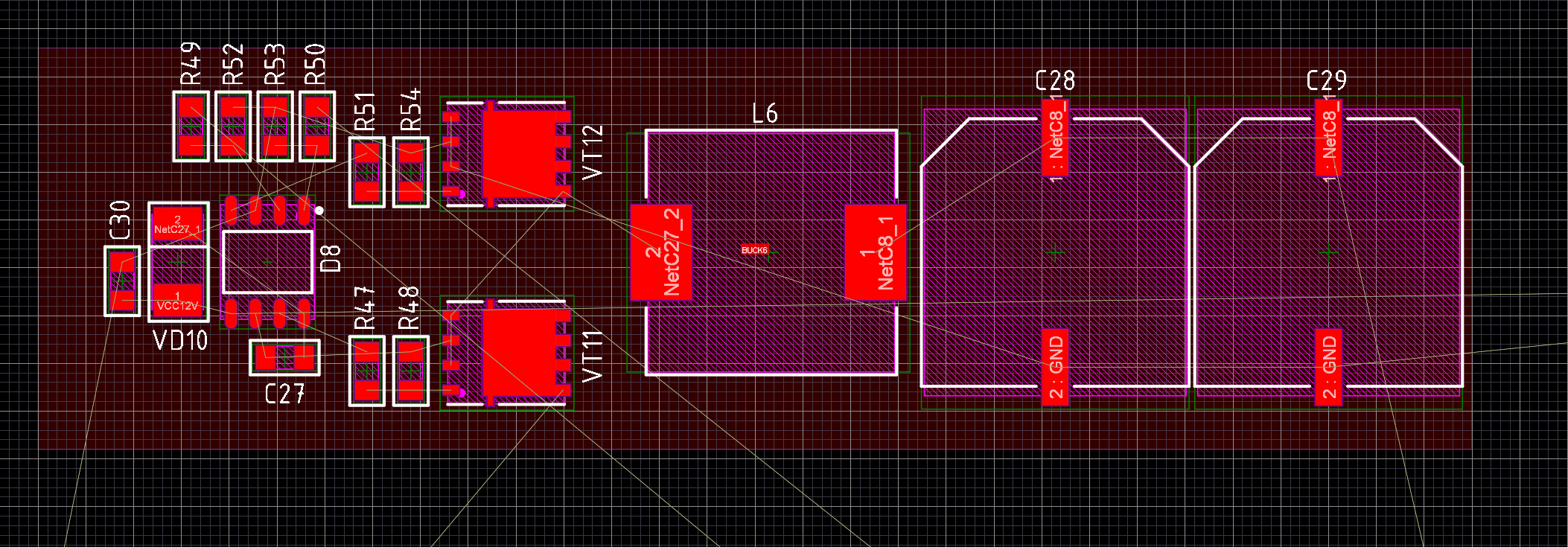
Now click Execute Changes and as a result we get the following PCB:
As you can see on the board appeared 6 red zones, which are called rooms (Room). In each room are electronic components for one channel and nothing more. Now you need to set the dimensions of the room, that is, specify what specific area will occupy the components of our channel and make the layout of parts. It looks like this:
So the components of each channel will be located and that is exactly the area to occupy. True, something I do not like here ... Aha! The designations of the components in the silk-screen layer (white lettering) are not continuous numbering, but the numbering in the “Designation_ Room Name” format, that is, we have R6_BUCK1, R6_BUCK2 resistors and so on. I want to avoid the prefix "_BUCK1" and each component had its own number. Press Ctrl + L and then go to the Annotate Options menu, where we see this menu:
Now you need to choose the numbering option $ ComponentPrefix $ GlobalIndex and click OK. Click Reset All to drop all values and then click Anotate Designated . As we see in the channel BUCK2, the components changed their designations from R6_BUCK2 to the more familiar designations R6, R7, etc .:
It remains to agree with the changes by clicking Accept Changes and in the window that opens confirm all by clicking on Execute Changes . We transfer the changes from the scheme to the PCB Design -> Update PCB Documet as we have already done. As a result, we observe “human” designations that do not occupy the entire charge and spoil it:
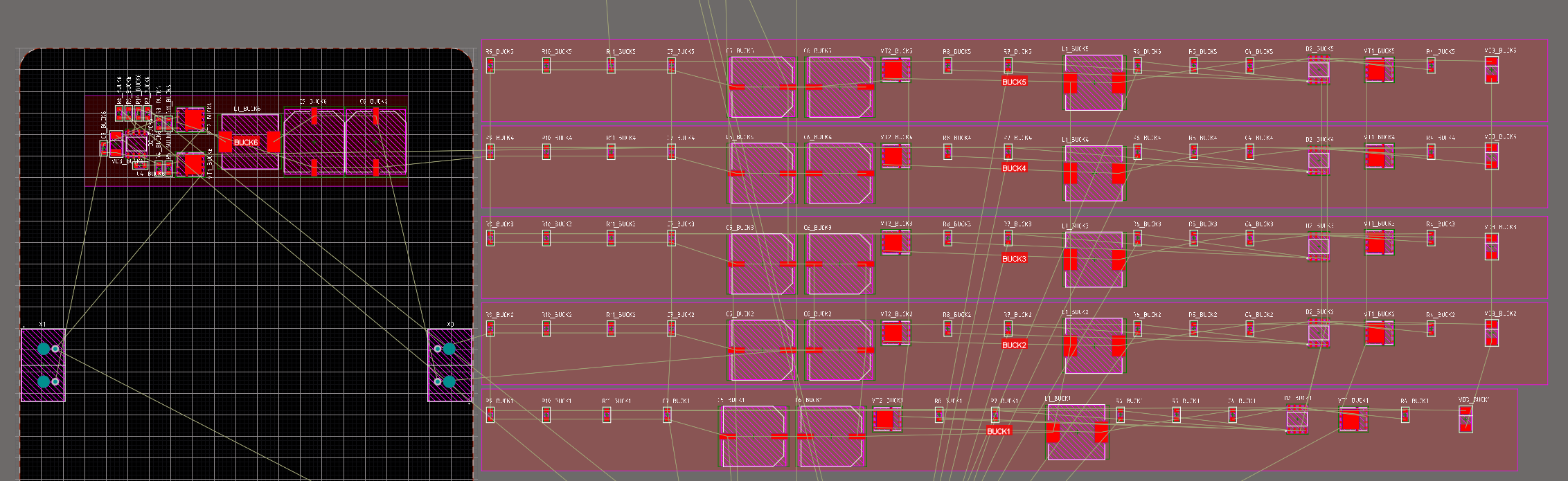
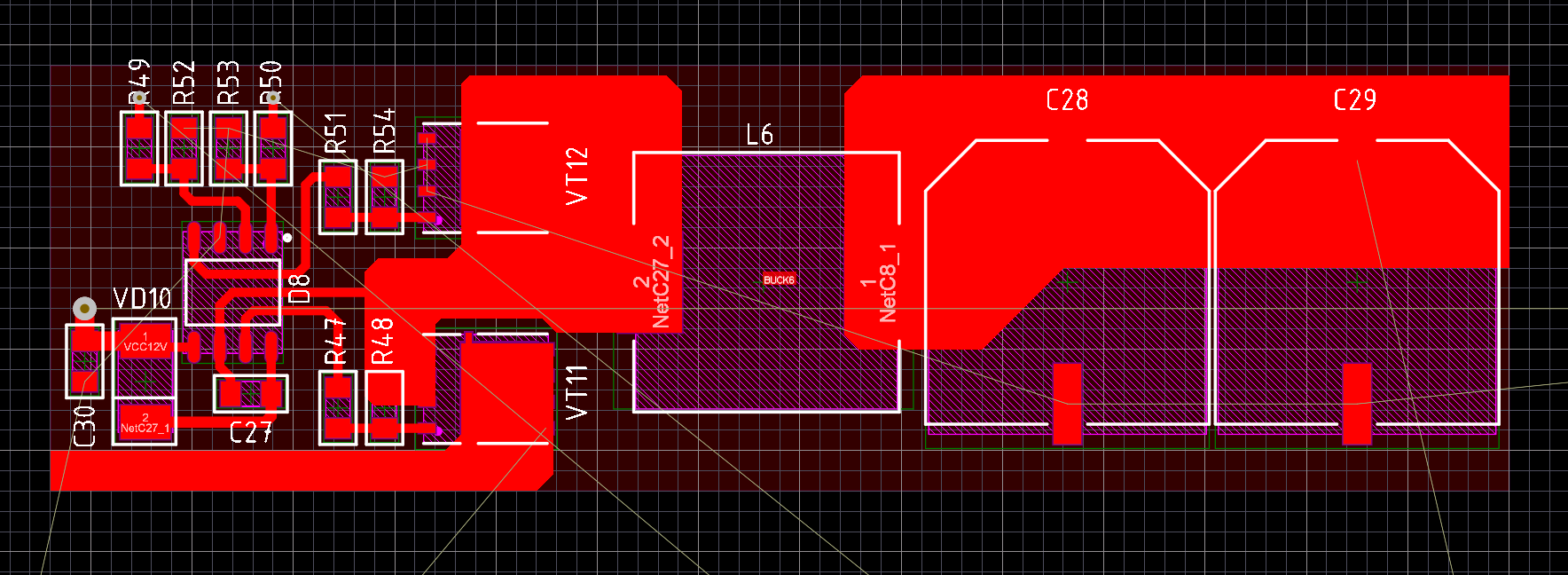
Having an adequate layout and designations go to the trace - let's trace the chains inside one room of “BUCK6” and get just such a picture:
I did not plant everything, GND left untouched, because This is usually a single polygon filled. Enough to demonstrate. Now do the following:
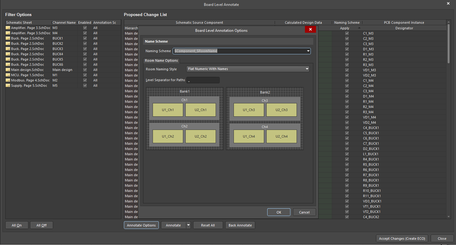
- Come Design -> Rooms -> Cope Room Format
- Altium tells us below the Choose source room , that is, it offers to poke into the room with which you need to copy everything, in my case in BUCK6
- Now altium suggests ChooseDestination Room , that is, asks to poke into the room in which to copy our layout. Choose any of the BUCKs.
- A menu opens in which you can tick the Apply To Specified Channel checkbox, which says that you need to copy not just to the selected room, but to all similar ones.
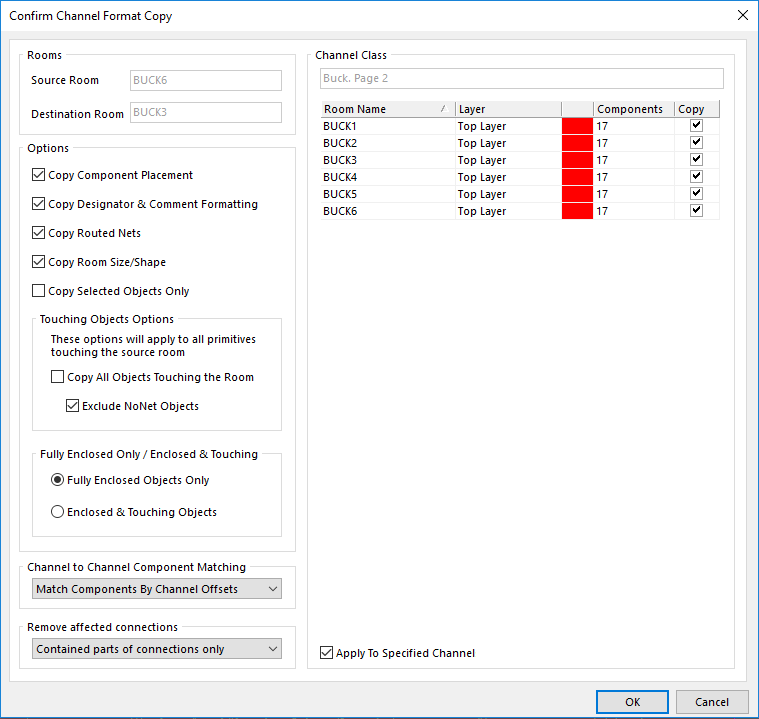
- Click OK and enjoy!
I didn’t check and chose 2 channels with clicks, since There are situations when, for example, not all channels are identical. Remember the VRM on the motherboard of the CPU, there are often 3-4 phases on the one hand, and 3-4 more on the other. In my case, these can be 3 phases with one wiring and 3 more phases with another. I think the general ideology is clear. Now let's look at the result:
We observe 3 identical channels and most importantly - time I spent on all channels as 1. In this abstract case, the time saving is 6 times, but in real tasks the order of reducing labor costs is about the same. Yes, and not unimportant factor - if you make 6 channels with your hands, then the "eye is washed out" because of the same type of work and it is likely to make a mistake or make a curve layout.
Total
I hope you were interested to learn about one of the basic design paradigms of electronics and get something new and useful for yourself. And remember - accuracy in the documentation, libraries and the use of the right tools in CAD will allow you to avoid mistakes and save a lot of time.
Source: https://habr.com/ru/post/426951/
All Articles