Download configuration to FPGA via USB or disassemble FTDI MPSSE

In the life of each pleisovod there comes a time when you need to write your own configuration file loader in the FPGA. I had to participate in the development of an educational stand for the department of a technical university. The stand is designed to study digital signal processing, although in this article it does not really matter. And what matters is that the stand is based on the FPGA (Altera Cyclone IV), on which, according to the idea of the stand's author, students assemble all kinds of DSP schemes. The stand is connected to the computer via USB. Required to download FPGA from a computer via USB.
The decision to connect to a PC to use FTDI in its dual channel form - FT2232H was made. One channel will be used to configure the FPGA, the other can be used for high-speed exchange in FIFO mode.
FTDI has a MORPH-IC-II debugging board, where the Cyclone II FPGA is flashed via USB. Schematic diagrams are freely available. The source code of the loader is partially open: the loader itself is available, but all the logic of working with FTDI is moved to a private library and cannot be modified. To tell the truth, initially I planned to use this bootloader in my project, or, in extreme cases, make my shell based on their dll. The firmware is loaded into the FPGA in passive serial mode (passive serial - PS), FTDI operates in the MPSSE mode. The performance of the MORPH-IC-II solution was fully confirmed on the breadboard, but the problem, as it often happens, came from no one was waiting. It turned out that during the MORPH-IC-II dll operation all the connected FTDI devices are blocked, and as part of the training complex there are two more devices with similar converters: a generator and a signal analyzer. Simultaneous work with them is not possible. Damn weird and annoying.
A similar case is implemented in the guys from the Mars Rover : USB JTAG programmer MBFTDI . There, FTDI is also used in the MPSSE mode, but unlike MORPH-IC-II, work with FPGAs occurs in the JTAG mode. The source code is freely available, but I did not find a clear indication of their status (license). Therefore, I did not raise my hand in a commercial project.
I will correct such a mistake, everything that will be presented within the framework of this article is laid out in an open repository under the BSD license.
Downloading the configuration file to the FPGA chip
The first step is to deal with the FPGA boot mode. For those who are just starting to get acquainted with the topic, I will spend a little excursion. Although the Altera (Intel) FPGA of the Cyclone IV E family is installed on my board, the boot methods are similar for the entire FPGA Cyclone group, and it is suspected that they are suitable for many other families in one form or another.
FPGA of this type uses volatile SRAM to store configuration data. This configuration data defines the functionality of the final device. In professional jargon, this data is often referred to as "firmware." Thus, the firmware is stored in a special RAM and each time the device is turned on it must be loaded into the FPGA chip. There are several ways (configuration schemes) with which the firmware can be loaded into SRAM (the list is relevant for Cyclone IV E):
- Active serial (AS).
- Active parallel (Active parallel (AP)).
- Passive serial (Passive serial (PS)).
- Fast passive parallel (FPP)).
- JTAG.
The choice of a specific mode of loading is carried out using the external conclusions of the FPGA (MSEL group). JTAG mode is always available. Active mode implies that when powering the FPGA it reads data from external memory (serial or parallel) independently. In the passive mode, the FPGA waits for the external media to proactively transfer configuration data to it. These schemes fit well into the Master (Master) Slave concept. In active modes, FPGA acts as a master, and in passive modes - as a slave.
In this task, not the FPGA, but the user must decide when the firmware should be updated, therefore the download mode should be passive. And to save the legs of the chip, we select the serial interface. Passive sequential (PS) mode and JTAG are suitable here. The logic of JTAG is somewhat more complicated, so we will focus on the first option.
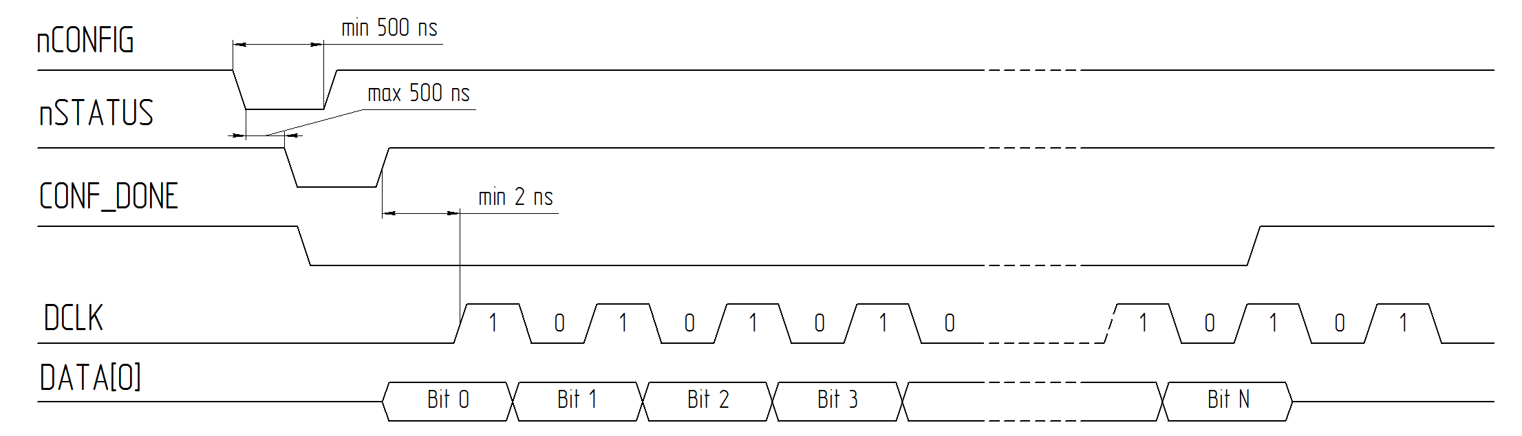
The figure below shows the scheme of connecting the FPGA to an external controller for downloading in PS mode.

To begin configuration, the external master controller must generate a low to high transition on the nCONFIG line. As soon as the FPGA is ready to receive data, it will form a high level on the nSTATUS line. After that, the master can start transmitting data on the DATA [0] line , and the corresponding clock pulses - on the DCLK line. The data must be transmitted to the target device until a high level is established on the CONF_DONE line (or the data does not run out), and the FPGA goes into the initialization state. It should be noted that after CONF_DONE is set to one, two more clock pulses must be applied in order for the FPGA to initialize.
The data is transmitted by the least significant digit ( LSB ) ahead, that is, if the configuration file contains the sequence 02 1B EE 01 FA (take the example as it is from the Handbook), a sequence should be formed on the data line:
0100-0000 1101-1000 0111-0111 1000-0000 0101-1111 Thus, only five lines are used: the DATA [0] and DCLK lines for serial transmission, the nCONFIG , nSTATUS , CONF_DONE lines for control.
At its core, the PS mode is nothing more than SPI with additional flag manipulation.
The data transfer rate should be lower than the maximum frequency specified in the documentation; for the Cyclone IV E project used in the project, it is 66 MHz.
The minimum transmission frequency does not exist, in theory it is possible to suspend the configuration indefinitely. This gives excellent opportunities for step-by-step debugging with the participation of an oscilloscope, which we will certainly use.
The figure below shows the timing diagram of the interface with the most significant timings.
Sly Beast MPSSE
Consider the operation of FTDI in MPSSE mode. The MPSSE (Multi-Protocol Synchronous Serial Engine) mode, in my opinion, is a more or less successful attempt to create some kind of serial interface designer, give the developer the opportunity to implement widely used data transfer protocols such as SPI, I2C, JTAG, 1-wire and many others based on them.
Currently, the mode is available for ICs: FT232H, FT2232D, FT2232H, FT4232H. I use the FT2232H in my project, so I’m talking more about it. For MPSSE mode, 16 legs are allocated, divided into two bytes: low L and high H. Each byte can be read or set. The four lower legs of the byte L have special functions — sequential data transfer can occur through them. Each foot can be configured as an input or output, a default value can be set for output. For serial transmission, the order of the bits ( MSB / LSB ), the length of the transmitted word, the frequency of clock pulses, the clock edge — forward (Rising) or rear (Falling) is configured; you can choose to transmit only clock pulses without data, or you can choose 3-phase clock (relevant for I2C) and much more.
Gently proceed to programming. There are two alternative ways of software interaction with FTDI chips: first, let's call it classic, in this case, when connected to the USB port, the chip in the system is defined as a virtual serial port (COM), the operating system uses the Virtual COM Port (VCP) driver. All further programming is no different from programming a classic COM port: opened - transmitted / counted - closed. And this is true for various operating systems, including Linux and Mac OS. However, with this approach, it will not be possible to realize all the capabilities of the FTDI controller - the chip will work as a USB-UART adapter. The second method is provided by the proprietary library FTD2XX, this interface provides special functions that are not available in the standard API COM port, in particular, setting and using special modes of operation are available, such as MPSSE, 245 FIFO, Bit-bang. The FTD2XX API library is well documented by the Software Application Development D2XX Programmer's Guide , widely and for a long time known in narrow circles. And yes, FTD2XX is also available for various operating systems.
The FTDI developers faced the task of putting a relatively new MPSSE into the existing D2XX software interaction model. And they succeeded; to work in the MPSSE mode, the same set of functions is used as for the other "classic" modes, the same FTD2XX API library is used.
In short, the algorithm of operation in the MPSSE mode can be described as follows:
- Find the device in the system and open it.
- Perform the initial chip initialization and transfer it to the MPSSE mode.
- Configure MPSEE operation mode.
- Direct work with data: transmit, receive, manage GPIO - we implement the target exchange protocol.
- Close the device.
We write the loader
We proceed to the practical part. In my experiments as IDE, I will use Eclipse version Oxygen.3a Release (4.7.3a), as a compiler - mingw32-gcc (6.3.0). Win7 operating system.
From the FTDI website we download the latest current version of the driver for your operating system. In the archive we find the header file ftd2xx.h with a description of all API functions. The API itself is implemented as ftd2xx.dll, but we will leave the dynamic import for later, and use static linking: we will need the ftd2xx.lib library file. For my case, ftd2xx.lib is in the i386 directory.
In Eclipse, create a new C project. Creating a makefile can be trusted with IDE. In the link settings, we specify the path and name of the ftd2xx library (I transferred the required files to the project directory in the ftdi daddy). I will not focus on the specifics of setting up a project for Eclipse, since I suspect that most people use other environments and compilers for programming under Win.
Point one. Find a device and open it.
FTD2XX API allows you to open a chip using one or another known information about it. This can be its serial number in the system: the first FTDI chip connected will take the number 0, the next 1, and so on. The number in the system is determined by the order of connection of microcircuits, to put it mildly, this is not always convenient. To open a chip by number, the FT_Open function is FT_Open . You can open the chip by its serial number ( FT_OPEN_BY_SERIAL_NUMBER ), description ( FT_OPEN_BY_DESCRIPTION ) or by location ( FT_OPEN_BY_LOCATION ), for this the function FT_OpenEx is FT_OpenEx . The serial number and description are stored in the internal memory of the chip and can be recorded there during the manufacture of the device in which FTDI is installed. The description, as a rule, characterizes the type of instrument or family, and the serial number must be unique for each product. Therefore, the most convenient way to identify the devices supported by the developed program is its description. We will open the FTDI chip by description (descriptor). In fact, if we initially know the chip descriptor string, then we don’t need to search for a device in the system, however, as an experiment, we will derive all devices connected to a computer with FTDI. Using the FT_CreateDeviceInfoList function, FT_CreateDeviceInfoList will create a detailed list of connected chips, and with the help of the FT_GetDeviceInfoList function, FT_GetDeviceInfoList consider it.
ftStatus = FT_CreateDeviceInfoList(&numDevs); if (ftStatus == FT_OK) { printf("Number of devices is %d\n",numDevs); } if (numDevs == 0) return -1; // allocate storage for list based on numDevs devInfo = (FT_DEVICE_LIST_INFO_NODE*)malloc(sizeof(FT_DEVICE_LIST_INFO_NODE)*numDevs); ftStatus = FT_GetDeviceInfoList(devInfo,&numDevs); if (ftStatus == FT_OK) for (int i = 0; i < numDevs; i++) { printf("Dev %d:\n",i); printf(" Flags=0x%x\n",devInfo[i].Flags); printf(" Type=0x%x\n",devInfo[i].Type); printf(" ID=0x%x\n",devInfo[i].ID); printf(" LocId=0x%x\n",devInfo[i].LocId); printf(" SerialNumber=%s\n",devInfo[i].SerialNumber); printf(" Description=%s\n",devInfo[i].Description); } D:\workspace\ftdi-mpsse-ps\Debug>ftdi-mpsse-ps.exe Number of devices is 4 Dev 0: Flags = 0x0 Type = 0x5 ID = 0x4036001 LocId = 0x214 SerialNumber = AI043NNV Description = FT232R USB UART Dev 1: Flags = 0x2 Type = 0x6 ID = 0x4036010 LocId = 0x2121 SerialNumber = L731T70OA Description = LESO7 A Dev 2: Flags = 0x2 Type = 0x6 ID = 0x4036010 LocId = 0x2122 SerialNumber = L731T70OB Description = LESO7 B Dev 3: Flags = 0x2 Type = 0x8 ID = 0x4036014 LocId = 0x213 SerialNumber = FTYZ92L6 Description = LESO4.1_ER Three devices with FTDI chips are connected to my PC: FT232RL (type 0x5), FT2232H (type 0x6) and FT232H (tepe 0x8). The FT2232H chip in the system was displayed as two independent devices (Dev 1 and Dev 2). The PS FPGA interface is connected to Dev 2, its dexryptor is “LESO7 B”. Open it:
//Open a device with device description "LESO7 B" ftStatus = FT_OpenEx("LESO7 B", FT_OPEN_BY_DESCRIPTION, &ftHandle); if (ftStatus != FT_OK) { printf ("pen failure\r\n"); return -1; } Most API functions return the status of their call of type FT_STATUS , all possible values are described as enum in the header file. There are many of them, but it is enough to know that the value of FT_OK is the absence of error, all other values are error codes. A good programming style will check the status value after each API function call.
If the device was successfully opened, then in the variable ftHandle there appears some value other than zero, some equivalent of the file descriptor, which is used when working with files. The resulting handle establishes communication with the hardware interface and must be used when calling all library functions that require access to the chip.
In order to prove in practice the working capacity of the system for the current stage, we should go directly to point five of our algorithm.
After completing work with the chip, it must be closed. The function FT_Close used for this:
FT_Close(ftHandle); Item 2. Initialize the chip and enable MPSSE
The setting is typical for most modes and is well described in the AN_135 FTDI MPSSE Basics documentation.
- Perform a reset (resets) chip. Function
FT_ResetDevice. - In case there is some garbage lying around in the receive buffer, we clear it.
FT_Purgefunction. - Adjust the size of buffers for reading and writing.
FT_SetUSBParametersfunction. - Disable parity check.
FT_SetChars. - We set the read and write timeouts. By default, timeouts are disabled, we enable timeout for transmission.
FT_SetTimeouts. - We configure the waiting time for sending a packet from the chip to the host. By default, 16 ms, we accelerate to 1 ms.
FT_SetLatencyTimer. - Enable stream control for inbound requests.
FT_SetFlowControl. - Everything is ready to activate the MPSSE mode. We reset the MPSSE controller. Use the function
FT_SetBitMode, set the mode to 0 (mode = 0, mask = 0). - Enable MPSSE mode. Function
FT_SetBitMode- mode = 2, mask = 0.
The opening and configuration of the chip are combined into the MPSSE_open function, and as a parameter, we pass the string with the handle of the device being opened:
static FT_STATUS MPSSE_open (char *description) { FT_STATUS ftStatus; ftStatus = FT_OpenEx(description, FT_OPEN_BY_DESCRIPTION, &ftHandle); if (ftStatus != FT_OK) { printf ("open failure\r\n"); return FT_DEVICE_NOT_OPENED; } printf ("open OK, %d\r\n", ftHandle); printf("\nConfiguring port for MPSSE use...\n"); ftStatus |= FT_ResetDevice(ftHandle); //Purge USB receive buffer first by reading out all old data from FT2232H receive buff: ftStatus |= FT_Purge(ftHandle, FT_PURGE_RX); //Set USB request transfer sizes to 64K: ftStatus |= FT_SetUSBParameters(ftHandle, 65536, 65536); //Disable event and error characters: ftStatus |= FT_SetChars(ftHandle, 0, 0, 0, 0); //Sets the read and write timeouts in milliseconds: ftStatus |= FT_SetTimeouts(ftHandle, 0, 5000); //Set the latency timer to 1mS (default is 16mS): ftStatus |= FT_SetLatencyTimer(ftHandle, 1); //Turn on flow control to synchronize IN requests: ftStatus |= FT_SetFlowControl(ftHandle, FT_FLOW_RTS_CTS, 0x00, 0x00); //Reset controller: ftStatus |= FT_SetBitMode(ftHandle, 0x0, FT_BITMODE_RESET); //Enable MPSSE mode: ftStatus |= FT_SetBitMode(ftHandle, 0x0, FT_BITMODE_MPSSE); if (ftStatus != FT_OK) { printf("Error in initializing the MPSSE %d\n", ftStatus); return FT_OTHER_ERROR; } Sleep(50); // Wait for all the USB stuff to complete and work return FT_OK; } Item 3. Configure MPSEE operation mode.
Actually, at this stage, the MPSSE processor is activated and ready to receive commands. Commands are byte sequences, the first byte of which is "op-code", followed by the command parameters. The command may have no parameters and consist of one "op-code". Commands are transmitted using the FT_Write function, the response from the MPSSE processor can be obtained using the FT_Read function.
After each command sending, it is useful to subtract the processor's response, since in case of an incorrect command, the answer may contain an error message - the 0xFA symbol. The "bad command - 0xFA response" mechanism can be used to synchronize an application program with an MPSSE processor. If everything is OK, then the chip will return the symbol 0xFA to the obviously erroneous command. Op-code is described in Command Processor for MPSSE and MCU Host Bus Emulation Mode .
MPSSE tuning is reduced to setting the data transfer rate, direction and initial states of the I / O lines.
Consider setting the MPSSE processor's transfer rate. The setting for chips with support for Full-speed mode only (FT2232 D ) and chips with High-speed (FT2232 H , FT232H, FT4232H) occurs somewhat differently. In the outdated FT2232D, a 12 MHz clock is used, and in modern ones - 60 MHz. Hence the formula for calculating the data transfer rate:
where f core is the FTDI core frequency, Divisor is a two-byte divider, which, in fact, sets the data clocking frequency.
As a result, if the divisor is zero, then the maximum data transfer rate will be 30 Mbps, and the minimum data transfer rate will be at 65535 divider - 458 bps.
The calculation of the divisor is entrusted to the preprocessor. The macro returns the divisor:
#define FCORE 60000000ul #define MPSSE_DATA_SPEED_DIV(data_speed) ((FCORE/(2*data_speed)) -1) And these two macros return the high and low bytes of the divider, respectively:
#define MPSSE_DATA_SPEED_DIV_H(data_speed) ((MPSSE_DATA_SPEED_DIV(data_speed)) >> 8) #define MPSSE_DATA_SPEED_DIV_L(data_speed) \ (MPSSE_DATA_SPEED_DIV(data_speed) - (MPSSE_DATA_SPEED_DIV_H(data_speed)<< 8)) In addition, it should be noted that in modern chips for compatibility with the old man FT2232D there is an additional divider of 5, which turns 60 MHz into 12 MHz. This divider is activated by default, in our case it should be disabled.
We find the corresponding op-code (0x8A) and a helmet command to the processor:
BYTE byOutputBuffer[8], byInputBuffer[8]; DWORD dwNumBytesToRead, dwNumBytesSent = 0, dwNumBytesRead = 0; byOutputBuffer[0] = 0x8A; ftStatus = FT_Write(ftHandle, byOutputBuffer, 1, &dwNumBytesSent); Sleep(2); // Wait for data to be transmitted and status ftStatus = FT_GetQueueStatus(ftHandle, &dwNumBytesToRead); ftStatus |= FT_Read(ftHandle, byInputBuffer, dwNumBytesToRead, &dwNumBytesRead); if (ftStatus != FT_OK) { printf("Error\r\n"); return FT_OTHER_ERROR; } else if (dwNumBytesToRead > 0) { printf("dwNumBytesToRead = %d:", dwNumBytesToRead); for ( int i = 0; i < dwNumBytesToRead; i++) printf (" %02Xh", byInputBuffer[i]); printf("\r\n"); return FT_INVALID_PARAMETER; } return FT_OK; As an experiment, instead of the actual command 0x8A, send the value 0xFE, which does not correspond to any op-code, console output:
dwNumBytesToRead = 2: FAh FEh The processor returned two bytes, the byte "bad command" - 0xFA and the value of this "bad" command. Thus, by sending several commands at once, we will be able not only to track the fact of the error itself, but also to understand on which command this error occurred.
In order not to deal with "magic numbers" in the future, we will arrange all op-code in the form of constants and put it in a separate header file.
To fully configure the mode, you must specify the direction of the I / O lines and their default value. Let us turn to the concept of connection. In order not to clutter up an already bloated article, I crossed out a fragment of the scheme of interest:
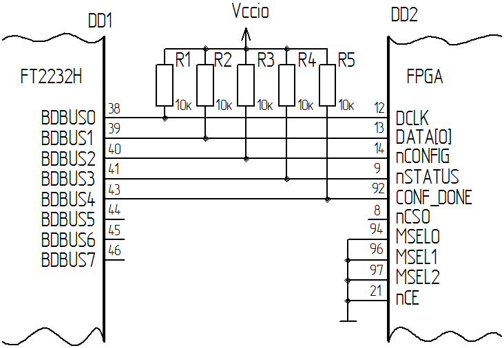
The DCLK , DATA [0] , nCONFIG lines must be configured as outputs, and the nSTATUS , CONF_DONE lines as inputs. According to the diagram, we determine what initial states the lines should have. For clarity, the pinout of the scheme is summarized in the table:
| FPGA pin | Pin name | Pin | MPSSE | Direction | default |
|---|---|---|---|---|---|
| DCLK | BDBUS0 | 38 | TCK / SK | Out | 0 |
| DATA [0] | BDBUS1 | 39 | TDI / DO | Out | one |
| nCONFIG | BDBUS2 | 40 | TDO / DI | Out | one |
| nSTATUS | BDBUS3 | 41 | TMS / CS | In | one |
| CONF_DONE | BDBUS4 | 43 | GPIOL0 | In | one |
All used lines are located on the low byte of the MPSSE port. To set the value, use op-code 0x80. This command assumes two arguments: the first following the op-code byte is a bitwise value, and the second is the direction (one is the port to be output, zero is the port to be input).
As part of the struggle with the "magic number", all the ordinal numbers of the lines and their default values will be in the form of constants:
#define PORT_DIRECTION (0x07) #define DCLK (0) #define DATA0 (1) #define N_CONFIG (2) #define N_STATUS (3) #define CONF_DONE (4) // initial states of the MPSSE interface #define DCLK_DEF (1) #define DATA0_DEF (0) #define N_CONFIG_DEF (1) #define N_STATUS_DEF (1) #define CONF_DONE_DEF (1) It remains only to make sure that the TDI - TDO loop is disabled (can be activated for testing) and issue a separate function:
static FT_STATUS MPSSE_setup () { DWORD dwNumBytesToSend, dwNumBytesSent, dwNumBytesToRead, dwNumBytesRead; BYTE byOutputBuffer[8], byInputBuffer[8]; FT_STATUS ftStatus; // Multple commands can be sent to the MPSSE with one FT_Write dwNumBytesToSend = 0; // Start with a fresh index byOutputBuffer[dwNumBytesToSend++] = MPSSE_CMD_DISABLE_DIVIDER_5; byOutputBuffer[dwNumBytesToSend++] = MPSSE_CMD_DISABLE_ADAPTIVE_CLK; byOutputBuffer[dwNumBytesToSend++] = MPSSE_CMD_DISABLE_3PHASE_CLOCKING; ftStatus = FT_Write(ftHandle, byOutputBuffer, dwNumBytesToSend, &dwNumBytesSent); dwNumBytesToSend = 0; // Reset output buffer pointer // Set TCK frequency // Command to set clock divisor: byOutputBuffer[dwNumBytesToSend++] = MPSSE_CMD_SET_TCK_DIVISION; // Set ValueL of clock divisor: byOutputBuffer[dwNumBytesToSend++] = MPSSE_DATA_SPEED_DIV_L(DATA_SPEED); // Set 0xValueH of clock divisor: byOutputBuffer[dwNumBytesToSend++] = MPSSE_DATA_SPEED_DIV_H(DATA_SPEED); ftStatus |= FT_Write(ftHandle, byOutputBuffer, dwNumBytesToSend, &dwNumBytesSent); dwNumBytesToSend = 0; // Reset output buffer pointer // Set initial states of the MPSSE interface // - low byte, both pin directions and output values /* | FPGA pin | Pin Name | Pin | MPSSE | Dir | def | | --------- | -------- | --- | ------ | --- | --- | | DCLK | BDBUS0 | 38 | TCK/SK | Out | 0 | | DATA[0] | BDBUS1 | 39 | TDI/DO | Out | 1 | | nCONFIG | BDBUS2 | 40 | TDO/DI | Out | 1 | | nSTATUS | BDBUS3 | 41 | TMS/CS | In | 1 | | CONF_DONE | BDBUS4 | 43 | GPIOL0 | In | 1 | */ // Configure data bits low-byte of MPSSE port: byOutputBuffer[dwNumBytesToSend++] = MPSSE_CMD_SET_DATA_BITS_LOWBYTE; // Initial state config above: byOutputBuffer[dwNumBytesToSend++] = (DCLK_DEF << DCLK) | (DATA0_DEF << DATA0) | (N_CONFIG_DEF << N_CONFIG) | (N_STATUS_DEF << N_STATUS) | (CONF_DONE_DEF << CONF_DONE); // Direction config above: byOutputBuffer[dwNumBytesToSend++] = PORT_DIRECTION; ftStatus |= FT_Write(ftHandle, byOutputBuffer, dwNumBytesToSend, &dwNumBytesSent); // Send off the low GPIO config commands dwNumBytesToSend = 0; // Reset output buffer pointer // Set initial states of the MPSSE interface // - high byte, all input, Initial State -- 0. // Send off the high GPIO config commands: byOutputBuffer[dwNumBytesToSend++] = MPSSE_CMD_SET_DATA_BITS_HIGHBYTE; byOutputBuffer[dwNumBytesToSend++] = 0x00; byOutputBuffer[dwNumBytesToSend++] = 0x00; ftStatus |= FT_Write(ftHandle, byOutputBuffer, dwNumBytesToSend, &dwNumBytesSent); // Disable loopback: byOutputBuffer[dwNumBytesToSend++] = MPSSE_CMD_DISABLE_LOOP_TDI_TDO; ftStatus |= FT_Write(ftHandle, byOutputBuffer, dwNumBytesToSend, &dwNumBytesSent); Sleep(2); // Wait for data to be transmitted and status ftStatus = FT_GetQueueStatus(ftHandle, &dwNumBytesToRead); ftStatus |= FT_Read(ftHandle, byInputBuffer, dwNumBytesToRead, &dwNumBytesRead); if (ftStatus != FT_OK) { printf("Unknown error in initializing the MPSSE\r\n"); return FT_OTHER_ERROR; } else if (dwNumBytesToRead > 0) { printf("Error in initializing the MPSSE, bad code:\r\n"); for ( int i = 0; i < dwNumBytesToRead; i++) printf (" %02Xh", byInputBuffer[i]); printf("\r\n"); return FT_INVALID_PARAMETER; } return FT_OK; } Item 4. We implement the download protocol
It seems everything is ready for practical experiments. First, we check that the initialization is performed correctly, in the main program body we call MPSSE_open() and MPSSE_setup() , and before closing the device ( FT_Close ) we place an empty getchar() . Run the program and use the oscilloscope to make sure that the default levels are set on all the PS lines. By changing the value of these levels in the initialization (nothing terrible will happen with the FPGA), we make sure that the desired MPSSE processor is the real thing - everything works adequately and you can proceed to the data transfer.
Sequential sending and receiving of data is performed in command mode using the same op-code. The first byte of the command is the op-code, which determines the type of operation, followed by the length of the transmitted or received sequence and, if it is a transmission, the data itself. The MPSSE processor can transmit and receive data, also do it simultaneously. The transmission may be either the least significant bit forward (LSB) or the most significant (MSB). Data transmission can occur either on the leading or trailing edge of clock pulses. For each combination of options there is its own op-code, each bit of op-code describes the mode of operation:
| Bit | Function |
|---|---|
| 0 | Synchronization on the front of the record: 0 - positive, 1 - negative |
| one | 1 - work with bytes, 0 - work with bits |
| 2 | Synchronization on the front for reading: 0 - positive, 1 - negative |
| 3 | Transfer Mode: 1 - LSB, 0 - MSB first |
| four | TDI data transmission |
| five | Reading data from TDO line |
| 6 | TMS data transfer |
| 7 | Must be 0, otherwise it is a different group of commands. |
When configuring the FPGAs using the PS scheme, data transfer occurs on the leading edge in LSB mode. , , op-code 0001_1000b 0x18 . ( , ), . : . , , 0, 65536, 65535. , . MPSSE_send .
static BYTE byBuffer[65536 + 3]; static FT_STATUS MPSSE_send(BYTE * buff, DWORD dwBytesToWrite) { DWORD dwNumBytesToSend = 0, dwNumBytesSent, bytes; FT_STATUS ftStatus; // Output on rising clock, no input // MSB first, clock a number of bytes out byBuffer[dwNumBytesToSend++] = MPSSE_CMD_LSB_DATA_OUT_BYTES_POS_EDGE; // 0x18 bytes = dwBytesToWrite -1; byBuffer[dwNumBytesToSend++] = (bytes) & 0xFF; // Length L byBuffer[dwNumBytesToSend++] = (bytes >> 8) & 0xFF; // Length H memcpy(&byBuffer[dwNumBytesToSend], buff, dwBytesToWrite); dwNumBytesToSend += dwBytesToWrite; ftStatus = FT_Write(ftHandle, byBuffer, dwNumBytesToSend, &dwNumBytesSent); if (ftStatus != FT_OK ) { printf ("ERROR send data\r\n"); return ftStatus; } else if (dwNumBytesSent != dwNumBytesToSend) { printf ("ERROR send data, %d %d\r\n", dwNumBytesSent, dwNumBytesToSend); } return FT_OK; } — 65 , - , op-code . byBuffer , buff , , op-code . , , .
, "" , 25 , , , 1 ( , #define DATA_SPEED 1000000ul ). :
BYTE byOutputBuffer[] = {0x02, 0x1B, 0xEE, 0x01, 0xFA}; MPSSE_send(byOutputBuffer, sizeof(byOutputBuffer)); ( ):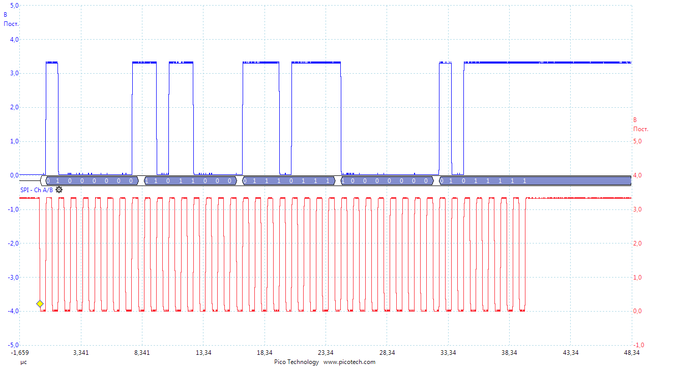
— DATA[0] , — DCLK . . , , .
, SPI ( ). , PS, . nCONFIG , nSTATUS , CONF_DONE . — , , — , .
MPSSE_get_lbyte , , .
static FT_STATUS MPSSE_get_lbyte(BYTE *lbyte) { DWORD dwNumBytesToSend, dwNumBytesSent, dwNumBytesToRead, dwNumBytesRead; BYTE byOutputBuffer[8]; FT_STATUS ftStatus; dwNumBytesToSend = 0; byOutputBuffer[dwNumBytesToSend++] = MPSSE_CMD_GET_DATA_BITS_LOWBYTE; ftStatus = FT_Write(ftHandle, byOutputBuffer, dwNumBytesToSend, &dwNumBytesSent); Sleep(2); // Wait for data to be transmitted and status ftStatus = FT_GetQueueStatus(ftHandle, &dwNumBytesToRead); ftStatus |= FT_Read(ftHandle, lbyte, dwNumBytesToRead, &dwNumBytesRead); if ((ftStatus != FT_OK) & (dwNumBytesToRead != 1)) { printf("Error read Lbyte\r\n"); return FT_OTHER_ERROR; // Exit with error } return FT_OK; } , op-code , . , - , , . , . MPSSE_set_lbyte :
static FT_STATUS MPSSE_set_lbyte(BYTE lb, BYTE mask) { DWORD dwNumBytesToSend, dwNumBytesSent; BYTE byOutputBuffer[8], lbyte; FT_STATUS ftStatus; ftStatus = MPSSE_get_lbyte(&lbyte); if ( ftStatus != FT_OK) return ftStatus; // Set to zero the bits selected by the mask: lbyte &= ~mask; // Setting zero is not selected by the mask bits: lb &= mask; lbyte |= lb; dwNumBytesToSend = 0; // Set data bits low-byte of MPSSE port: byOutputBuffer[dwNumBytesToSend++] = MPSSE_CMD_SET_DATA_BITS_LOWBYTE; byOutputBuffer[dwNumBytesToSend++] = lbyte; byOutputBuffer[dwNumBytesToSend++] = PORT_DIRECTION; ftStatus = FT_Write(ftHandle, byOutputBuffer, dwNumBytesToSend, &dwNumBytesSent); if ((ftStatus != FT_OK) & (dwNumBytesSent != 1)) { printf("Error set Lbyte\r\n"); return FT_OTHER_ERROR; } return FT_OK; } , . : FTDI; MPSSE; rbf- , nCONFIG , N_STATUS ; rbf- ; , , CONF_DONE . , MPSSE FTDI . , nCONFIG "" , , , .
int main(int argc, char *argv[]) { FT_STATUS ftStatus; BYTE lowByte; DWORD numDevs; // create the device information list if ( argv[1] == NULL) { printf ("NO file\r\n"); return -1; } frbf = fopen(argv[1],"rb"); if (frbf == NULL) { printf ("Error open rbf\r\n"); return -1; } ftStatus = FT_CreateDeviceInfoList(&numDevs); if ((numDevs == 0) || (ftStatus != FT_OK)) { printf("Error. FTDI devices not found in the system\r\n"); return -1; } ftStatus = MPSSE_open ("LESO7 B"); if (ftStatus != FT_OK) { printf("Error in MPSSE_open %d\n", ftStatus); EXIT(-1); } MPSSE_setup(); if (ftStatus != FT_OK) { printf("Error in MPSSE_setup %d\n", ftStatus); EXIT(-1); } printf ("nConfig -> 0\r\n"); MPSSE_set_lbyte(0, 1 << N_CONFIG); printf ("nConfig -> 1\r\n"); MPSSE_set_lbyte(1 << N_CONFIG, 1 << N_CONFIG); if (MPSSE_get_lbyte(&lowByte) != FT_OK) { EXIT(-1); } if (((lowByte >> N_STATUS) & 1) == 0) { printf("Error. FPGA is not responding\r\n"); EXIT(-1); } int i = 0; size_t readBytes = 0; // Send the configuration file: do { readBytes = fread(buff, 1, MPSSE_PCK_SEND_SIZE, frbf); if (MPSSE_send(buff, readBytes) != FT_OK) EXIT(-1); putchar('*'); if (!((++i)%16)) printf("\r\n"); } while (readBytes == MPSSE_PCK_SEND_SIZE); printf("\r\n"); memset(buff, 0x00, sizeof(buff)); MPSSE_send(buff, 1); // ? printf("Load complete\r\n"); // wait CONF_DONE set // A low-to-high transition on the CONF_DONE pin indicates that the configuration is // complete and initialization of the device can begin. i = 0; do { if (MPSSE_get_lbyte(&lowByte) != FT_OK) { printf ("Error read CONF_DONE\r\n"); EXIT(-1); } if (i++ > TIMEOUT_CONF_DONE) { printf ("Error CONF_DONE\r\n"); EXIT(-1); } Sleep(2); } while (((lowByte >> CONF_DONE) & 1) == 0); printf("Configuration complete\r\n"); FT_Close(ftHandle); fclose(frbf); } :
pen "LESO7 B" OK nConfig -> 0 nConfig -> 1 ** Load complete Configuration complete rbf- . . 30 / .
, - JTAG.
Materials on the topic
- FTDI-MPSSE-Altera PS . .
- . . .
- Software Application Development D2XX Programmer's Guide . FTDI. API D2XX.
- FTDI MPSSE Basics. Application Note AN_135 . . FTDI MPSSE. .
- Command Processor for MPSSE and MCU Host Bus Emulation Modes. Application Note AN_108 . op-code. .
- D2XX Drivers . FTDI.
')
Source: https://habr.com/ru/post/426131/
All Articles