Looking inside the Intel 8087 coprocessor
A little history of the development of a line of eight-bit processors manufactured by Intel
The line of eight-bit processors begins its history in April 1972. Intel 8008 was generally originally planned for use in calculators, I / O devices, but the manufacturer, after a good deal of thought, decided to find a new designation for the line - to be the central processor of a PC. Depending on the processor modifications, the clock frequency was 500 or 800 KHz, and the performance was 45000-160000 operations per second.
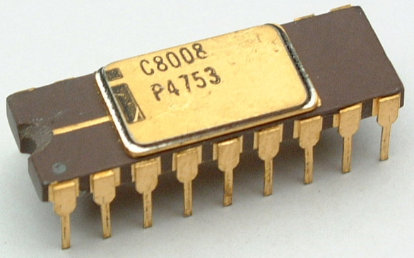
Intel C8008
In April 1974, Federico Faggini and Masatoshi Shima developed a new processor line - Intel 8080 . 6000 transistors were placed in a 40-pin ceramic package, a 16-bit address bus and an 8-bit data bus, and an addressable memory of 64 KB. The clock frequency was 2 MHz, and the performance was up to 500,000 operations per second. In order to make the use of the processor “comfortable,” an arithmetic co-processor, a clock generator, tire drivers, a timer, peripheral controllers, etc. were developed.
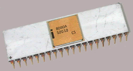
Intel 8080A
')
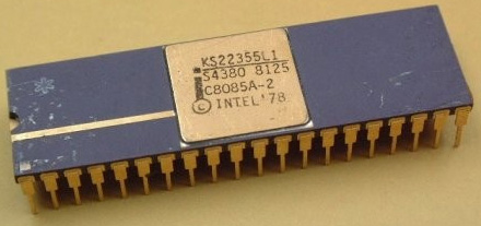
Two years later, in March 1976, the line of Intel 8085 saw the light: 6500 transistors were placed in a 40-pin ceramic (or plastic) package. The clock frequency ranged from 3 to 8 MHz, the data bus width was 8 bits, the address bus width was 16 bits, and the addressed memory was 64 Kb. This line was successfully "involved" in a PC or in the form of microcontrollers.
In June 1978, the production of the first line of 16-bit processors of the company, Intel 8086, began : 29000 transistors were placed on a 5.5 x 5.5 mm chip. The clock frequency was from 5 to 10 MHz, the performance was from 330 to 750 thousand operations per second, the data bus width was 16 bits, and the address bus width was 20 bits.
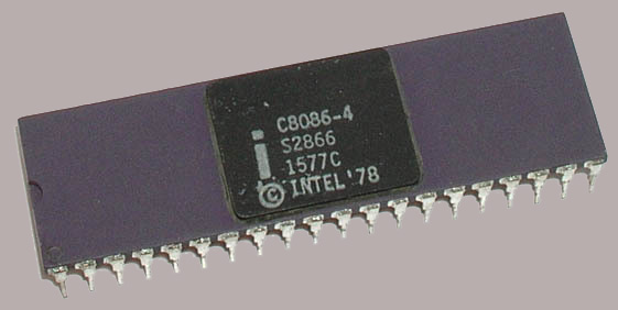
Intel 8086
A year later, in the summer of 1979, Intel released the 8088 line - a transitional link between 8 and 16-bit processors: 29,000 transistors, the clock frequency was 5-10 MHz. But the 8088 line has not become popular because of its high cost.
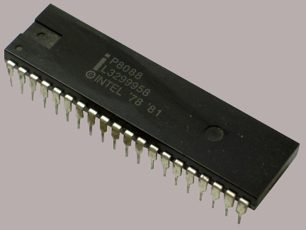
Intel P8088
8087 coprocessors
In June 1980, a line of Intel 8087 co-processors for Intel 8086, 8088 was released. Such co-processors contained 45,000 transistors, the clock frequency in various modifications ranged from 4 to 10 MHz.
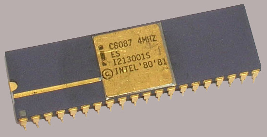
Intel C8087
A math coprocessor is a special module for performing floating point operations that works in conjunction with a central processor.
In order to save from such luxury as a coprocessor, they simply refused. But for solving time-consuming tasks, for example, the same engineering calculations, improving computer performance has become a necessity. It was possible to increase productivity at the expense of such a special module - a mathematical coprocessor.
According to INTEL, a math coprocessor can reduce the execution time of math operations, such as multiplication, division, and exponentiation, by 80 percent or more. The speed of performing simple mathematical operations, such as addition and subtraction, does not change.
Inside an Intel 8087 microprocessor chip
Looking inside the Intel 8087 floating point, I noticed an interesting feature on the chip: the formation of the substrate displacement. In this article I will explain how this circuit is implemented, using analog and digital circuits to create a negative voltage.
Intel developed the 8087 chip in 1980 in order to improve PC performance with 8086/8088 processor lines (such as the IBM PC) when performing floating point operations. Since the first microprocessors were designed to perform operations with integers, the execution of operations with floating-point numbers was slow, which already speak of performing transcendental operations, such as trigonometric functions or logarithms. The 8087 coprocessor significantly increased the speed of performing tasks with a floating point, everything was performed almost 100 times faster. The 8087 architecture was also implemented in later Intel processors, and the 8087 instructions are still used in modern x86 PCs.
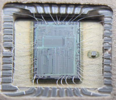
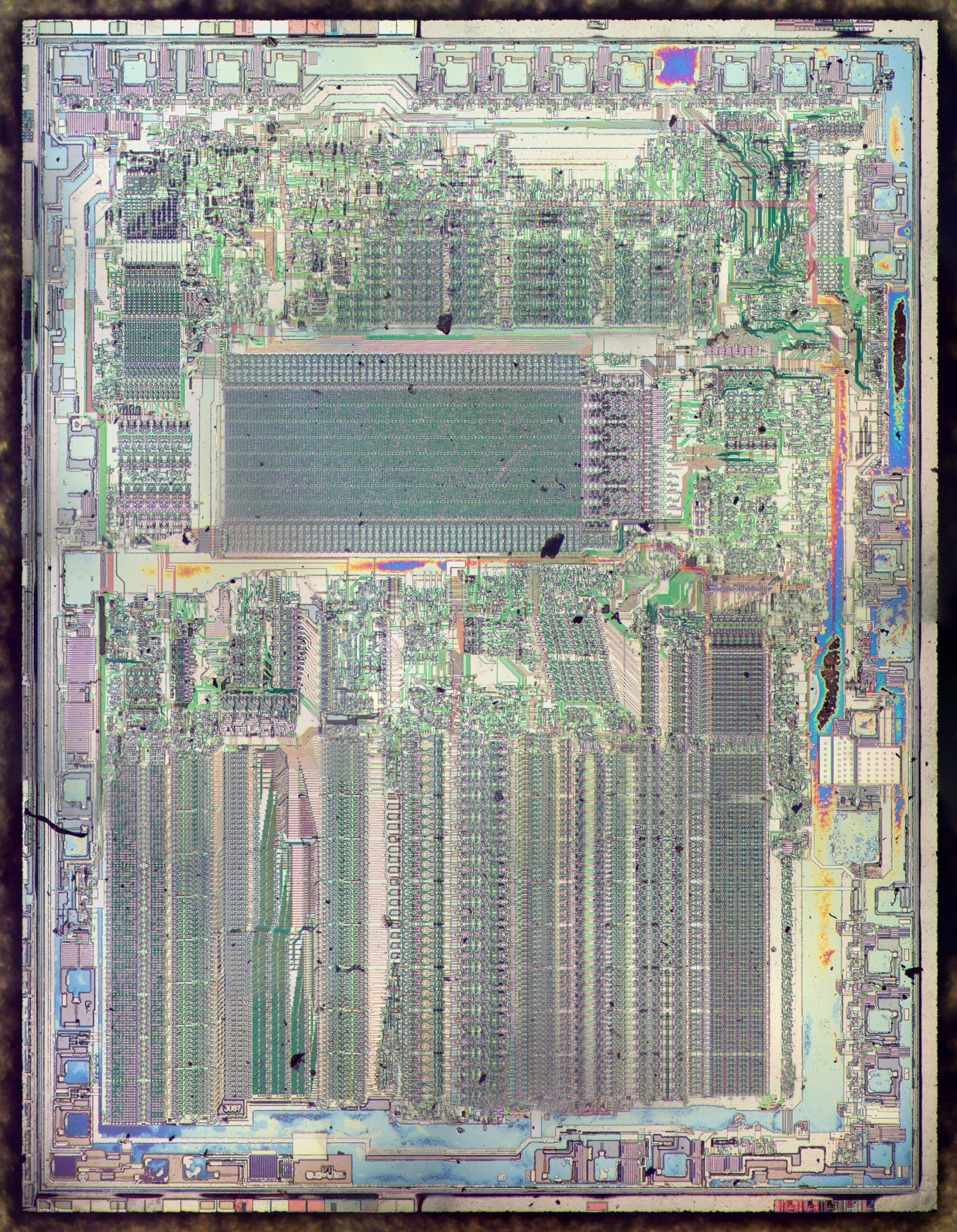
For the coprocessor, more than 60 new instructions were introduced, the name of which began with “F”, in order to distinguish them from the Intel 8086 integer instructions.I opened the 8087 chip and with the help of a highly productive microscope I took photographs, as a result of their arrangement I received the following image:

Crystal 8087 is very complex, contains 40,000 transistors (according to the statements of Intel) or 45,000 (according to Wikipedia). The photo shows the metal layer of the chip, the connections are located on top of the chip. The thickest white lines provide power and grounding of all parts of the chip. Under the metal layer - polysilicon or silicon, from which the chip transistors are formed.
In the lower half of the chip there is an expanded 80-bit arithmetic circuit: adder, registers, switches, mathematical constants. The large rectangle in the middle of the chip is microcode that implements the processor instruction set. At the top are the logic circuits and the bus circuitry, which is interfaced with the 8086 processor.
The black lines around the chip in the photograph are small thermocompression joints connecting the IC contact pads (metallized conductive areas of square or rectangular shape, located mainly along the periphery of the crystal or substrate) with 40 contacts on the crystal. Studying the technical description of 8087, it is not difficult to determine which contact pad on the matrix corresponds to which contact of the chip; 40 chip contacts (numbered counterclockwise) are connected to 40 pads on the chip.
Below is an enlarged image of a part of the matrix, on it we can better consider the contact pads. (Please note that the ground pins and +5 V power contact pads have several connections at the same time, which increases the amount of current supplied). But here is a “surprise” - there is an additional contact pad and a connection, located between the contact pads 40 and 1, and not connected to any of the contacts of the microcircuit.
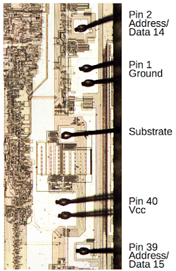
Looking at the thermocompression connection of the wire leads on the chip (below is an image), it turned out that the mysterious contact pad is not connected to any contact, but is connected to a small cube-shaped block. This "cube" is on the same metal base as the crystal, and is connected to the silicon substrate of the chip, the board.
I conducted an engineering analysis of the manufacturing technology in order to uncover the "secrets of the company" and came to the conclusion that this is part of the substrate 8087 displacement scheme, in which this compound is used to apply negative voltage to the substrate. How does this scheme work?
What is substrate displacement?
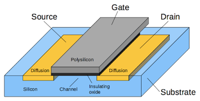
In the 1970s, high-density integrated circuits were built with n-MOS transistors (a field-effect transistor with an insulated gate and an n-type channel). The image below clearly demonstrates their structure. The base of the chip is silicon substrate. Transistors, in turn, also made of silicon. In order to change the type of conductivity and the concentration of carriers in the bulk of the semiconductor in order to obtain given properties, portions of silicon are doped with impurities to create diffusion regions with the desired properties. The transistor can be considered as a resistor that allows current to flow between the two diffusion regions of the source and drain. The transistor is controlled by a gate made of polysilicon. The input voltage at the gate controls the current flow from the source to the drain: a high voltage signal at the gate allows current to flow from the source to the drain, while a low signal voltage blocks the current. An insulating oxide layer separates the gate from the silicon beneath; the importance of this layer will be discussed a little later. These tiny transistors can be combined to form logic gates, microprocessor components, and other digital IC chips.
In high-performance integrated circuits, it was advantageous to apply a negative “bias” voltage on the substrate. To get this substrate bias voltage, many chips in the 1970s had an external contact that was connected to -5V. However, engineers did not like chips that require additional voltage. The chips of that era often needed three power sources. In addition, the number of contacts on the IC was limited (as a rule, only 18 contacts for memory chips). Therefore, the use of two more contacts for additional voltage was not a good solution. Part of the solution was found in the late 1970s: the chips generated a negative bias voltage inside. So there were chips that used one convenient power supply + 5V, and this clearly allowed the engineers to be "happier".
Inside the substrate offset circuit 8087
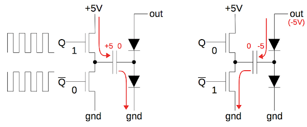
You may wonder how a chip can turn a positive voltage into a negative voltage. The answer is a charge pump called a charge pump. Uses capacitors as charge collectors, which are transferred from one capacitor to another using a switch system. The bias “generator” in 8087 has two charge pumps operating in turn. The diagrams below show the operation of one such charge pump. The charge pump is controlled by an oscillating signal (Q) and its inversion (Q). At the first stage, the upper transistor is turned on, as a result of which the capacitor is charged up to 5 volts relative to the ground. The second stage is the place where the magic happens. The lower transistor turns on by connecting the high voltage side of the capacitor to ground. Since the capacitor is still charging up to 5 volts, the underside of the capacitor should now be -5 volts, creating the desired negative output voltage. When the oscillator turns over again, the upper transistor turns on and the cycle repeats. The charge pump has received this name, as it pumps the charge from the exit to the ground. The charge pump is similar to a manual water pump.
I looked at the chip under the microscope. The metal layer hides the transistors below, and this makes it difficult to view the circuit. But, after removing the metal layer with hydrochloric acid, I got to the layers of polysilicon and silicon, “discovered” transistors and capacitors, as shown below (Colored areas are just interferences, since some oxides were not completely removed). The photo below shows two charge pumps: one to the left of the contact pad and one to the bottom. Each charge pump in accordance with the scheme, has two diodes, a large capacitor and two transistors.
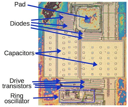
Capacitors are the most prominent feature of the substrate displacement circuit. Although in reality their dimensions are microscopic, they are huge by the standards for measuring the dimensions of a chip. The area for capacitors is approximately like a register memory of 72 bits (more than 400 transistors). Each capacitor consists of polysilicon over a silicon part, separated by an insulating oxide; polysilicon and silicon form capacitor plates. In the photo the capacitors are dotted with squares; These squares are contacts between polysilicon (or silicon) and the metal layer on top. (The metal layer is not visible because it was erased).
Four control transistors are high power transistors. Their sizes exceed the usual transistors. The red lines are polysilicon compounds that form the shutter. The green lines are the contacts to the metal layer that connect the transistors to +5 V or ground. The diodes near the contact pad are formed of transistors when the gate and drain are connected.
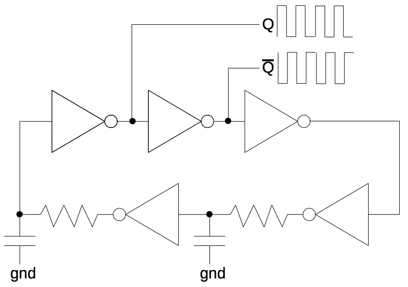
Charging pumps are driven by a circular oscillator, as shown in the image below. This circular oscillator consists of five inverters in a short circuit loop. Since the number of inverters is odd, the system is unstable and will oscillate. For example, if the input for the first inverter is 0, the output of the fifth inverter will be 1. To slow down the oscillation speed, there are two resistive-capacitive circuits in a circle. Since it takes some time to charge and discharge the capacitor, the oscillations will slow down, which will give time for the charge pump to work.
Before expanding the information about the circular oscillator, I will demonstrate how the standard NMOS inverter is implemented in silicon. Below is the inverter, its schematic representation and how it is embodied on the chip. The inverter uses a transistor and a load resistor (which is actually a transistor). If the input signal is low, the transistor is turned off, then the load resistor provides up to +5 V to the output. If the input signal is high, the transistor is turned on, the output voltage is applied to ground. Thus, the circuit inverts the input.
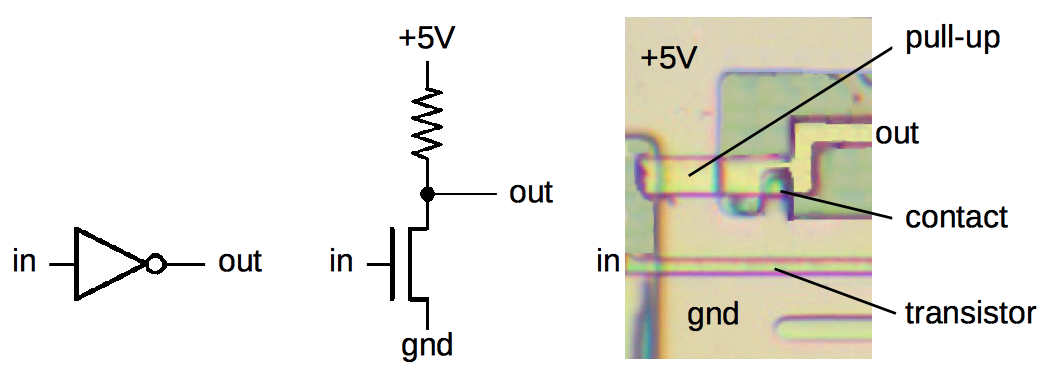
Doped silicon in the image is a large area of beige color. Thin yellow areas, near purple, - polysilicon. The input is a polysilicon wire. Where it intersects with silicon doped, it forms the gate of the transistor between the ground (below the input) and the output (above the input). A load resistor is implemented in a transistor that has a gate and drain connected together; This contact forms this connection between the transistor polycrystalline silicon gate and its silicon drain. Polysilicon also forms an output wire. Thus, the inverter on the chip is implemented with two transistors.
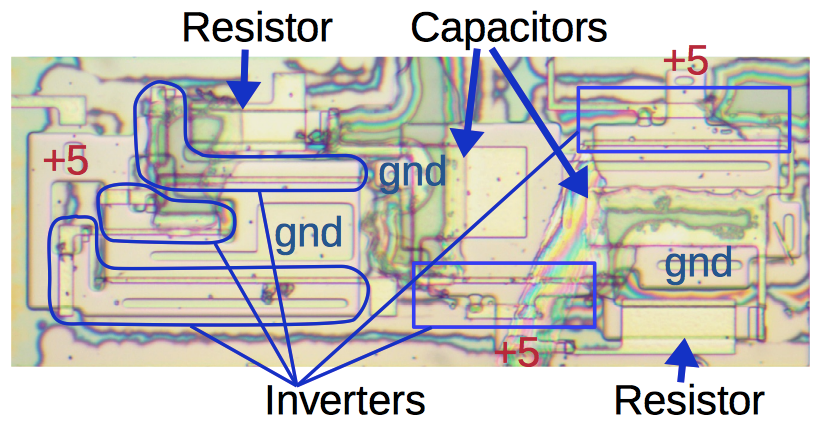
The photo above shows how a circular oscillator is formed on a crystal. All five inverters are shown. Each inverter has a different direction, which optimizes the structure. Resistors and capacitors of an RC circuit are also indicated. Resistors are simply transistors with a large distance between the source and drain, reducing the movement of current. Capacitors are designed like charge pump capacitors, but much smaller in size; Silicon on the bottom and polysilicon form the top of the capacitor plate, separated by a thin insulating oxide layer.
findings
An 8087 substrate-on-chip bias voltage generator is an interesting combination of a digital circuit (circular oscillator formed of inverters) and an analog charge pump. The bias voltage generator circuits of the substrate were introduced in the late 1970s, which made it possible for memory chips and microprocessors to work from a single +5 V power supply. This was much more convenient than using three different voltage sources. The substrate bias generator produces a negative voltage from a positive supply voltage using a charge pump.
Although the bias voltage generator may seem unclear in the computer history of the 1970s, this process is still part of modern integrated circuits, although everything has become much more complicated.
Despite the fact that the Intel 8087 floating-point chip was developed and put into operation 38 years ago, its “influence” is perceptible today. Due to its appearance, the IEEE 754 standard was adopted - the “IEEE standard that describes the format for representing floating-point numbers. Used in software (compilers from different programming languages) and hardware (CPU and FPU) implementations of arithmetic operations (mathematical operations). " Instructions 8087 remain part of the x86 processors.
Notes and links
1. For the coprocessor, more than 60 new instructions were introduced, the name of which began with “F”, in order to distinguish them from the Intel 8086 integer instructions. For example, analogs of the ADD / MUL / CMP commands in 8087 looked like FADD / FMUL / FCOM . These instructions were implemented using the escape command 8086, which was designed to allow the 8086 processor to communicate with the coprocessor.
The emergence of a coprocessor led to the creation of the IEEE 754 standard in 1985 for floating point arithmetic;
2. The imposition of a negative bias voltage on the substrate had several advantages. This reduced the parasitic capacitance, which accelerated the operation of the chip, made the threshold voltage of the transistor more predictable and reduced the leakage current.
3. In the past, DRAM and microprocessor chips often required three voltage sources: + 5V (Vcc), + 12V (Vdd) and -5V (Vbb). In the late 1970s, improved chip manufacturing technology allowed the use of a single power source. For example, the MK4116 from Mostek (16-kilobyte DRAM since 1977) required three voltage sources, while the improved MK4516 (1981) worked on one +5 V, thereby simplifying hardware design. The same thing happened with Intel chips: 2116 DRAM (16K, 1977) using three voltages and an improved 2118 (1979) - one voltage. The well-known Intel 8080 microprocessor (1974) used transistors operating in the enrichment mode, so it required three voltages. The improved version, 8085 (1976), used transistors with a depletion mode and was powered from a single power source of +5 V.
4. The third (+12 V) power supply in old chips has nothing to do with the substrate displacement. This source was used because in the early MOS-integrated circuits there were transistors operating in the enrichment mode, increasing the voltage on the gates. These transistors could not draw signals up to +5 V, they added an even higher power source of +12 V. In the mid-1970s, a new technology (ion implantation) allowed the creation of transistors operating in a depletion mode, the need for +12 V was exhausted.
5. I simplified the material a bit when discussing the charge pump. Due to the voltage drop in the transistors, the substrate voltage is likely to be around -3 V, not -5 V. By the direction of the pump, I mean current. If you think of this as pumping electrons, negative electrons are pumped in the opposite direction of the substrate.
Thank you for staying with us. Do you like our articles? Want to see more interesting materials? Support us by placing an order or recommending to friends, 30% discount for Habr users on a unique analogue of the entry-level servers that we invented for you: The whole truth about VPS (KVM) E5-2650 v4 (6 Cores) 10GB DDR4 240GB SSD 1Gbps from $ 20 or how to share the server? (Options are available with RAID1 and RAID10, up to 24 cores and up to 40GB DDR4).
VPS (KVM) E5-2650 v4 (6 Cores) 10GB DDR4 240GB SSD 1Gbps until December for free if you pay for a period of six months, you can order here .
Dell R730xd 2 times cheaper? Only we have 2 x Intel Dodeca-Core Xeon E5-2650v4 128GB DDR4 6x480GB SSD 1Gbps 100 TV from $ 249 in the Netherlands and the USA! Read about How to build an infrastructure building. class c using servers Dell R730xd E5-2650 v4 worth 9000 euros for a penny?
Source: https://habr.com/ru/post/424889/
All Articles