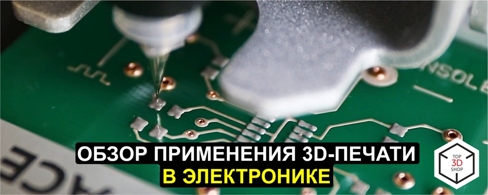
Overview of the use of 3D printing in electronics
3D printing seems to many to be something like a fantastic universal production method with which you can create anything: you just need to load a model, wait a while, and here it is - a product ready to use.
In some areas, in particular in mechanical engineering, this has already been implemented: the vast majority of 3D printers are focused on printing with one type of material, for example, thermoplastic polymers or metals, which is quite enough for the production of mechanical parts.

Mechanical products and their parts can even be made using inexpensive personal 3D printers.
')
As soon as we are faced with the need to manufacture a product consisting of different types of materials, there is a need for more complex specialized equipment. The area dealing with such products is electronics.
3D printing is already used in electronics today, and in the production of individual electronic components, additive manufacturing has significant advantages over traditional methods, despite the fact that the use of 3D printing in electronics began quite recently - the first 3D printer for printing electronic components was sold in 2015.
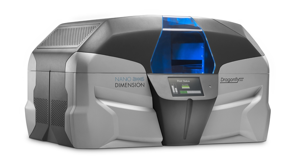
The Nano Dimension Dragonfly 2020 is the first professional-grade 3D printer for additive PCB production.
The use of 3D printing in electronics can be divided into two areas:
1. 3D printing of electronic components themselves: printed circuit boards, antennas, etc .;
2. Production of enclosures and other accessories for electronics.
3D printing of electronic components
Despite the fact that the integration of 3D printing into electronics production began quite recently, academic studies in this area were carried out relatively long ago, and the results of these works, in many ways, served as the basis for creating professional 3D printers for printing electronic components. The history of experimental developments in this area can be traced back to 1992.

Conductive pattern deposited by thermal spraying. The substrate is pre-sandblasted to ensure better adhesion of the sprayed material. From “Manufacturing mechatronics using thermal spray shape deposition” (J. Beck, F. Prinz, D. Siewiorek, LE Weiss, Proc. Solid Freeform Fabrication Symp., 1992, pp. 272-279).
Robokasting
In 2009, researchers at the University of Illinois (USA) developed conductive inks based on silver nanoparticles. When printing, such ink is extruded from a micro nozzle and deposited on a polymer substrate. Then, when heated to 150 ° C, silver particles agglomerate, forming a solid array, and the ink lines acquire conductivity. In this way, it becomes possible to create a drawing from conductors using the Direct Ink Writing method, connecting other electronic components with them, which is the basis for designing most electronic devices.
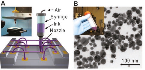
(A) - The design of the experimental setup for printing with conductive ink by the method of robocasting; (B) - Electron micrograph of silver nanoparticles in conductive ink.
Robokasting method consists in layer-by-layer formation of a product by extrusion of a pasty material (unlike the FDM method, in which a material melt is extruded). As a rule, the viscosity of such a material substantially depends on the shear stress: with a significant shear stress, the viscosity is small and the material is easily extruded from the nozzle; as the shear stress decreases, the viscosity becomes larger, so the product formed on the platform continues to retain its shape. Then the product can be subjected to additional heat treatment, to impart greater mechanical strength.

Schematic representation of the robokasting method: (A) - a 3D printer with several tanks for feeding materials into the print head, (B, C) —a nozzle and a layer structure of the product, characteristic of the robokasting method.
In 2011, the same group of researchers, conducting ink with a content of silver nanoparticles of 72% by weight, were used for 3D printing of miniature antennas, the need for which is increasing every year, due to the ubiquitous development of wireless technologies. Moreover, the printing of antennas was carried out on the surface of the hemisphere, and not on a flat table: this method of printing is called conformal 3D printing. Printing time of one antenna, depending on the speed, ranged from 0.5 to 3 hours. To achieve maximum conductivity, with a given ink composition, the printed antenna was heat treated at 550 ° C.
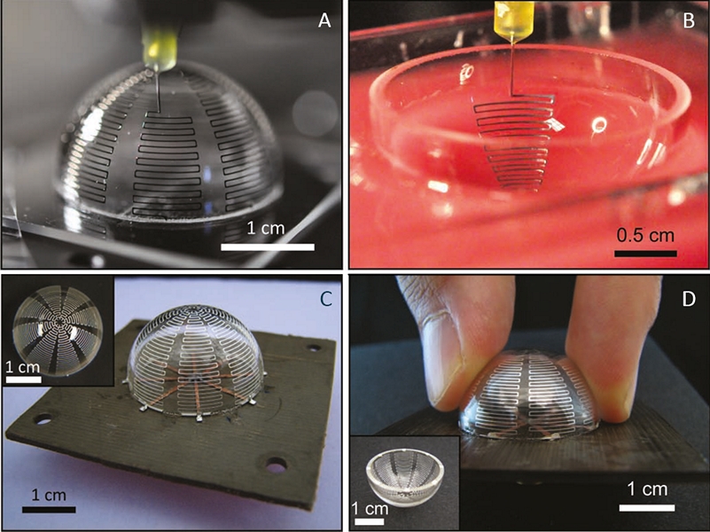
The process of printing the antenna of conductive material on the outer (A) and inner (B) surfaces of the glass hemisphere; (C, D) - the finished antenna.
A similar method of robocasting using conductive ink is also used for organizing interconnects on printed circuit boards: the base of a printed circuit board is produced using the FDM, SLS or SLA method, and then an electrically conductive pattern is formed on the surface of the circuit board. The manufacture of printed circuit boards using classical methods is a long process. If the design of the printed circuit board requires multi-stage optimization, then the production time of the prototype product is significantly increased. Therefore, the technology of rapid manufacture of printed circuit boards on the spot relevant to the developers of electronics.

The main stages of the production of electronic boards by the method of 3D printing and the finished board with electronic components, the base of which is made of Ultem 9085 by the FDM method.
3D printing greatly simplifies the transition from the classic planar layout of electronic devices to the volumetric layout , which allows much more efficient use of the volume for a dense layout of elements. This layout is most relevant in the aerospace industry.
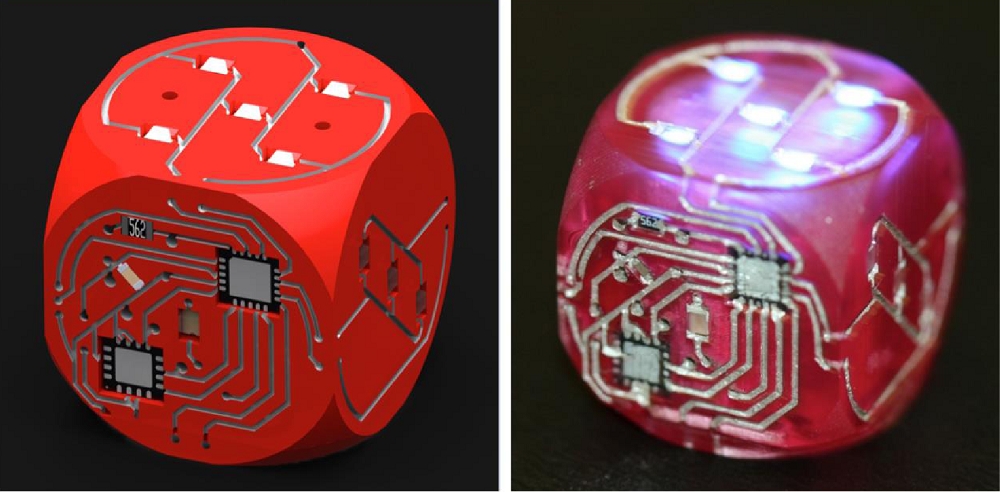
A six-sided electronic dice containing a microprocessor, an accelerometer and LEDs, in the creation of which the methods SLA (for printing a cube array) and DIW (for creating an electrically conductive pattern) were used.
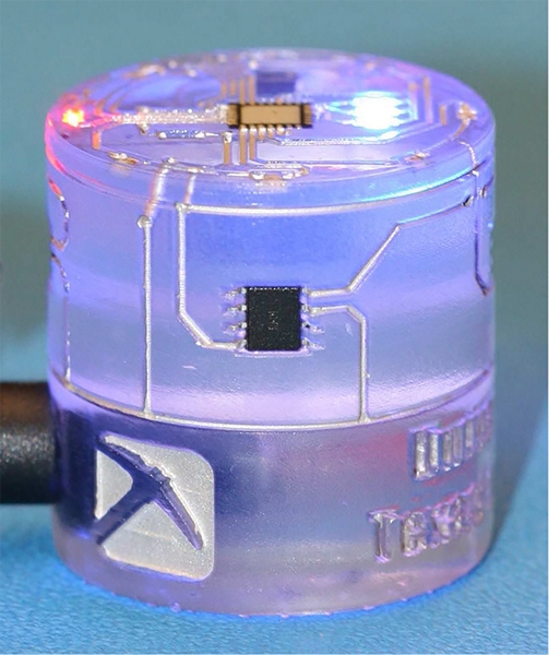
Hall sensor for measuring the magnetic field strength, made by the SLA method and robocasting.
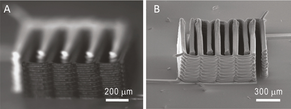
Lithium-ion microaccumulators made by robokasting.
3D printers for the production of printed circuit boards
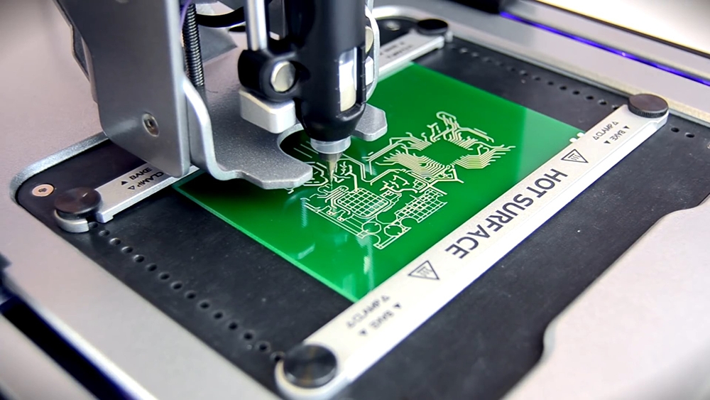
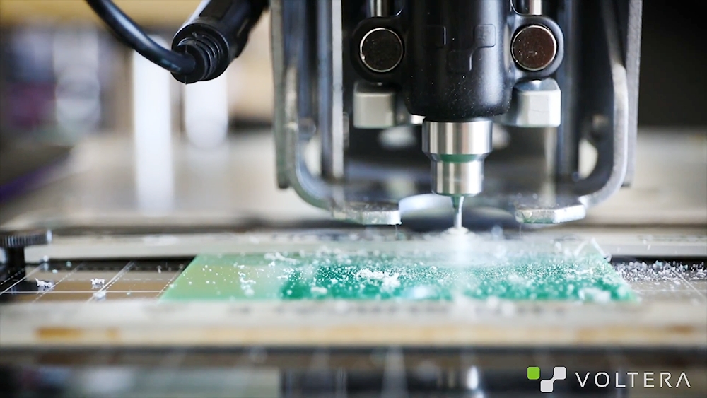
The production of electrically conductive patterns by robokasting found application in the Canadian company Voltara (Voltera), a compact personal V-One personal printer, designed for the production of printed circuit boards. Voltera V-One is a multifunctional device that combines the capabilities of a 3D printer and a CNC router.
Voltera V-One
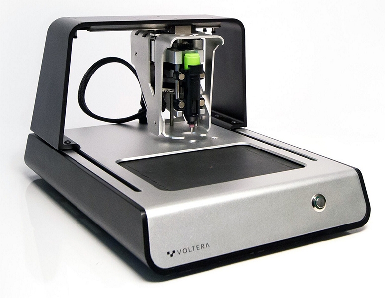
The appearance of the printer Voltera V-One.
Specifications
- Key features of the Voltera V-One:
- Overall dimensions, mm: (L × W × H) 390 × 257 × 207
- Weight, kg: 7
- Printing area, mm: 128 × 105
- Printing technology: robokasting (direct ink writing)
- Minimum track width, mm: 0.2
- The basis material of printed circuit boards: fiberglass FR4
- Maximum thickness of the printed circuit board, mm: 3
- Maximum temperature of the working platform, ° C: 240
- The composition of the solder paste: Sn (42%) / Bi (57.6%) / Ag (0.4%)
- Warm-up temperature in solder mode, ° C: 180-210
- Maximum spindle speed of drilling head, rpm: 13000
- Operating system: Windows 7, 8, 10 (64bit), OSX 10.11+
- File Format: Gerber
- Computer Interface: Wired USB
- Price, ₽: 637 872
In the first stage of the production of a printed circuit board using the V-One, a printed circuit board project in Gerber format (* .gbr), created, for example, using the Eagle software package, is loaded into the printer software.
PCB design in the Autodesk Eagle software package.
The design of the printed circuit board in the preparatory program for the Voltera V-One
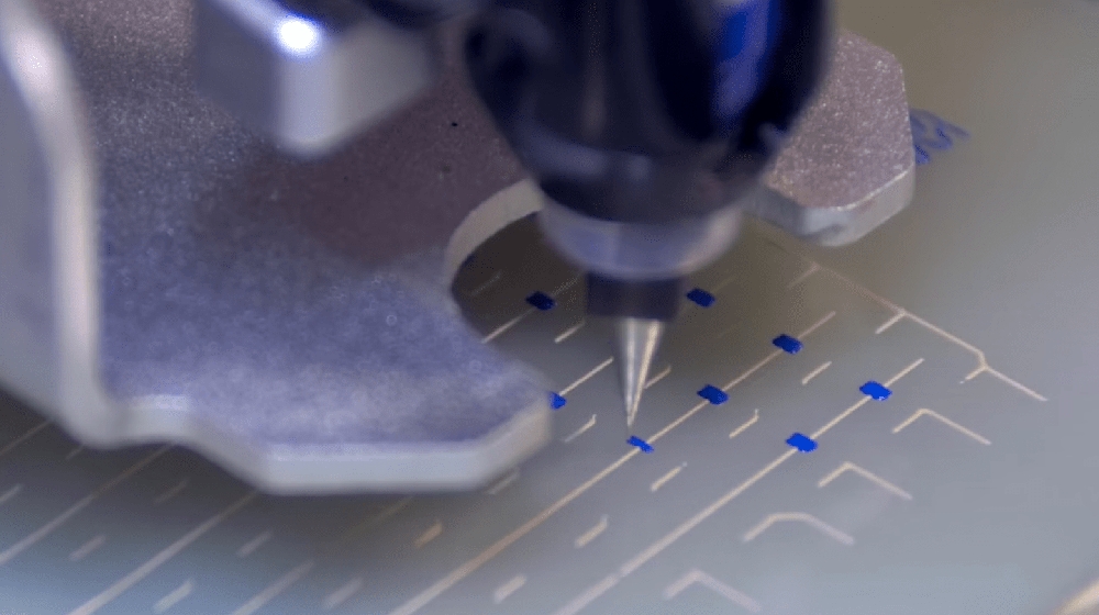
Then the base of the PCB board is fixed on the heated platform of the printer with the help of linear clamps, after which you can proceed to printing the conductive board pattern with special ink containing 90% of silver particles. The electrical parameters of such inks are suitable for digital devices and low-current electronics operating at frequencies up to 5 GHz.
Printing a conductive PCB pattern with special inks with a high silver content.
During printing, the paste is located in a replaceable syringe cartridge with a simple mechanical drive to feed the paste. One cartridge is enough for printing tracks with a total length of 100 meters, with a track width of 0.2 mm. Store the ink cartridge in the refrigerator.
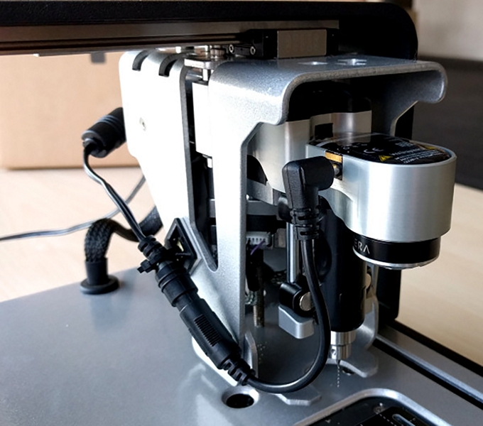
Voltera V-One printhead.
After the conductive layer is printed, the board is turned upside down with a conductive pattern and placed on the guides to prevent the platform surface, which is heated to cure the ink, from touching. Under the influence of heat conductive material passes from the pasty to the solid state. Drying ink takes about 30 minutes. When platform heating is turned on, the printer side lights change from blue to red to warn the operator.
V-One allows you to print double-layer cards that contain two conductive layers. Therefore, the printer is able to apply a dielectric material on top of the first conductive layer, to isolate it from the second conductive layer. Printing the second conductive layer occurs after drying a layer of insulating material.
The application of insulating material at the intersection of conductive layers during the production of a two-layer printed circuit board.
Changing the cartridge for printing with other material does not require disassembly and occurs very quickly, due to the fact that the cartridges are mounted on magnetic mounts.
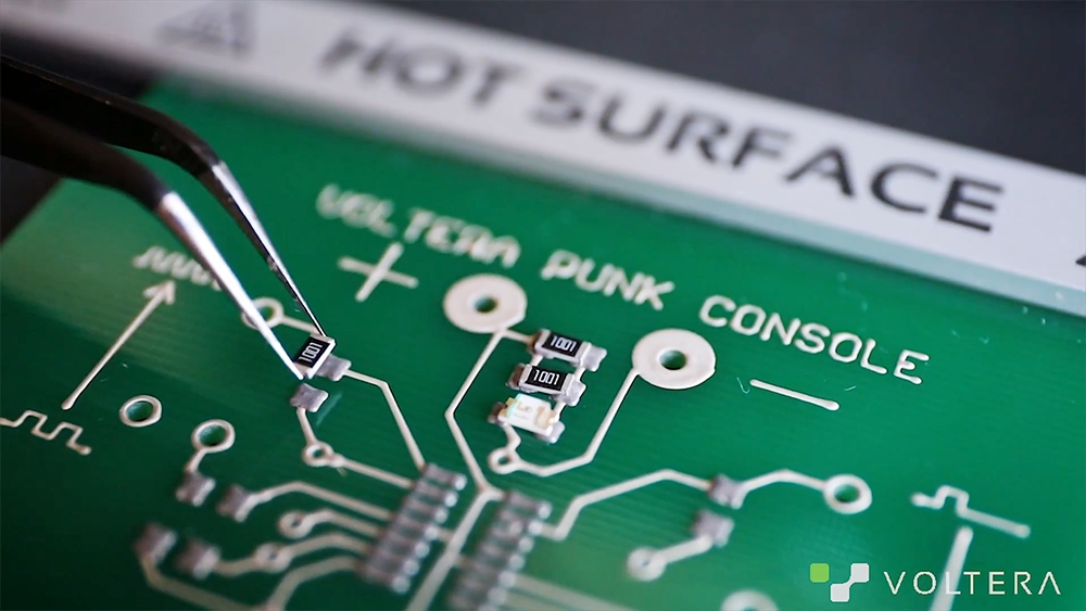
At the final stage, with the help of a printer, solder paste is applied in places where electronic components are mounted. Paste does not contain lead, which protects the health of the user. Paste can be applied not only on boards printed on the V-One, but also on boards with a ready-made conductive pattern.
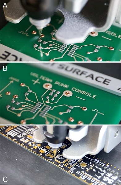
Applying solder paste after printing a conductive pattern: A - the process of applying solder paste to a board printed with the V-One; B - board, completely ready for mounting electronic components, C - applying solder paste to the board with a ready-made conductive pattern.
Placement on the printed circuit board of electronic components occurs manually.
After placing the electronic components on the board, the platform heats up and the components are soldered to the contact pads.
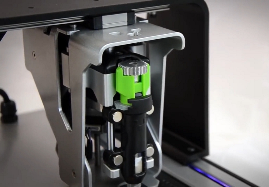
If a double-sided printed circuit board is required, which has a conductive pattern on both sides of the PCB (not to be confused with a two-layer one), then V-One provides the possibility of drilling holes in such a board using a special drilling head (the holes can be 0.7, 0.8, 0.9, 1.0 and 1.6 mm). The drilling head is a standalone module, the power of which is connected separately.
Drilling head Voltera V-One.
Drilling holes in the PCB using the Voltera V-One, before printing a conductive pattern.
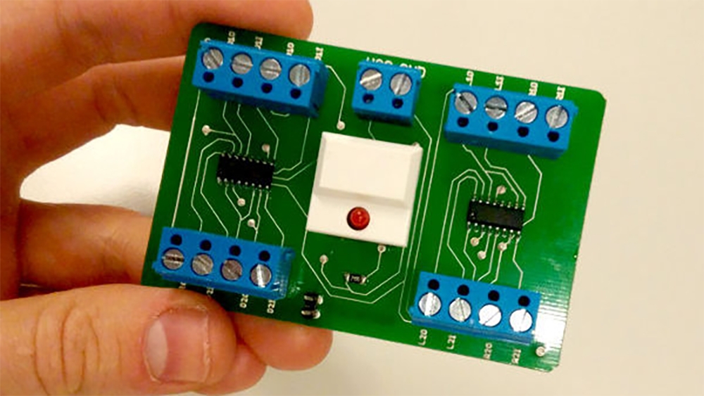
Fully finished electronic device made with the Voltera V-One
V-One can be used for printing any viscous compositions, which opens up opportunities for experimentation.
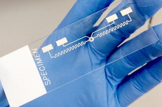
Printing in conductive ink on the glass surface with the Voltera V-One.
For printing with custom materials, you need to purchase a set of empty cartridges and accessories for refueling. You can print not only on PCB, but also on the surface of other materials resistant to temperatures of 200 ° C, at which conductive ink cures on glass, plastic plates or films. Standard inks are not suitable for printing flexible electronic devices, as they lose mechanical strength during repeated bending. The developers promise in the near future to submit a suitable composition for this purpose.
Another personal 3D printer for the production of electronic devices - Voxel8 , produced by the American company Voxel8 Inc. It is noteworthy that Voxel8 Inc. founded by a group of researchers from the University of Illinois, who in 2011 demonstrated the ability to print antennas in conductive ink (see the beginning of this review). A striking example of the successful implementation of the results of academic research in practical commercial products.
Voxel8 fully combines the functionality of a classic FDM printer and a DIW printer. Voxel8 is not focused on the production of printed circuit boards only; it is an FDM printer with the possibility of integrating electronic components into a product of any shape.
Voxel8
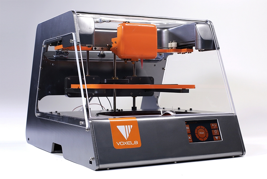
Appearance of the Voxel8 3D printer.
Specifications
- Print area volume: 150 × 150 × 100 mm
- Print technology: FDM, robokasting (direct ink writing)
- Layer height: 0.2 mm
- Materials to print: PLA, conductive ink
- Conductive ink cure time: 5 minutes
- The diameter of the filament, mm: 1.75
- Heated platform: yes
- Track width: 0.25 mm
- Software: Autodesk Project Wire, Euclid
- File format: STL
- Interface for computer connection: WiFi, Ethernet
- Price, ₽: 1,065,168
Since Voxel8 is designed for fully three-dimensional electronic devices, a special 3D editor, Autodesk Project Wire, created by the joint efforts of Autodesk and Voxel8, is used to place electronic components and connect them with conductors.
Project Wire allows you to import a 3D model of a future product without an electronic component. Then the user, in the Project Wire environment, places electronic components in the product volume, and the program automatically frees up space for them in the model. Electronic components can be selected from the Project Wire component database. After placement, the components are connected by conductive paths, the direction and shape of which can be edited by moving control points.

Project Wire program window for placing and connecting electronic components in the model volume.
Slicing model products with an integrated three-dimensional electronic circuit.
The base of the model is printed from PLA. The printer automatically interrupts printing for manual placement in an electronic component model. For ease of installation, the printer platform, along with the product, can be removed. Then printing resumes.

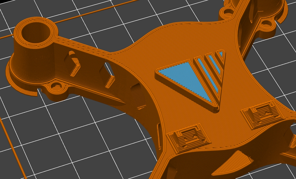
The press of the quadcopter with the 3D-electronic scheme.
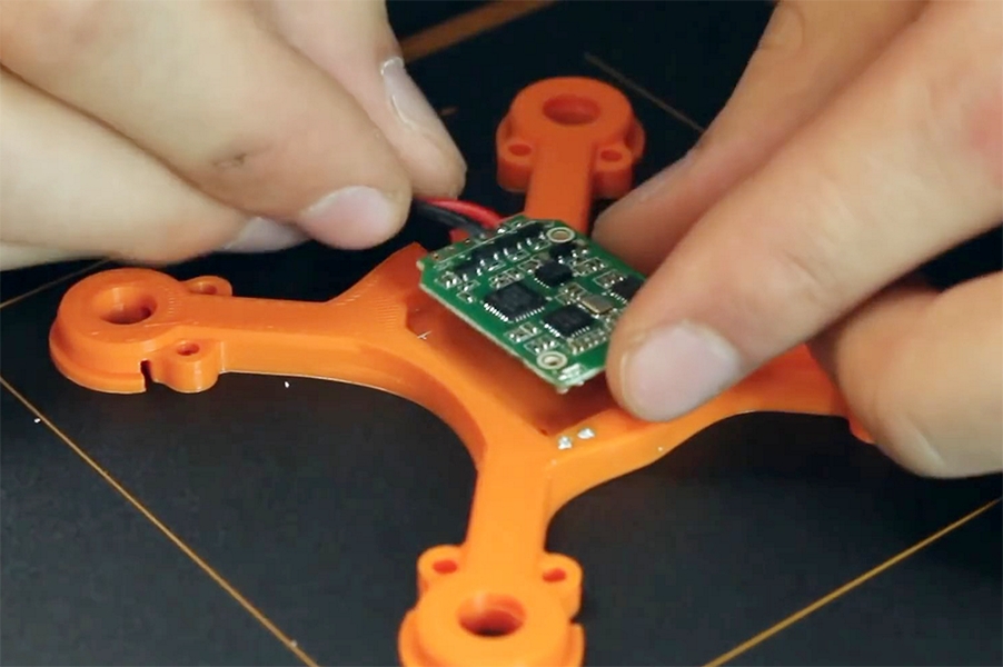
Installation of internal electronic components during printing.

Continuation of printing after installation of internal electronic components.

Photograph of a quadrocopter made using computed tomography, showing the spatial distribution of electronic components inside the device.

Model and finished electronic product made with Voxel8.
As a printer for the professional development of printed circuit board prototypes, consider the Nano Dimension DragonFly 2020 Pro .
DragonFly 2020 Pro
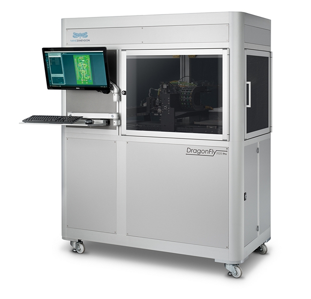
The appearance of the printer DragonFly 2020 Pro.
Specifications
- Overall dimensions, cm: (L × W × H) 140 × 80 × 180
- Weight, kg: 500
- Printing technology: inkjet
- Materials: conductive (based on silver nanoparticles) and dielectric ink
- Number of print heads: 2
- Track width, mm: 0.1 mm
- Volume of working space of the chamber, mm: 200 × 200 × 3
- Accuracy, mm: 0,001
- File Format: Gerber
- Possibility to print multilayer printed circuit boards: yes
- Operating system: Windows, Mac OS, Linux
DragonFly 2020 Pro prints not only the conductive pattern of the board, but also its base. It is printed from a dielectric resin, with properties close to FR4 fiberglass, therefore the product can be of any shape and contain mounting holes. Unlike personal printers for the manufacture of printed circuit boards, DragonFly 2020 Pro uses inkjet technology, which provides high precision manufacturing.
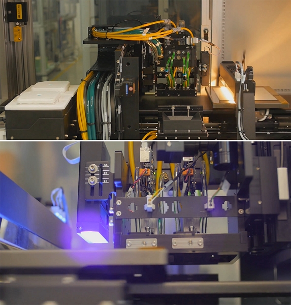
Both conductive and insulating materials are light cured during printing.
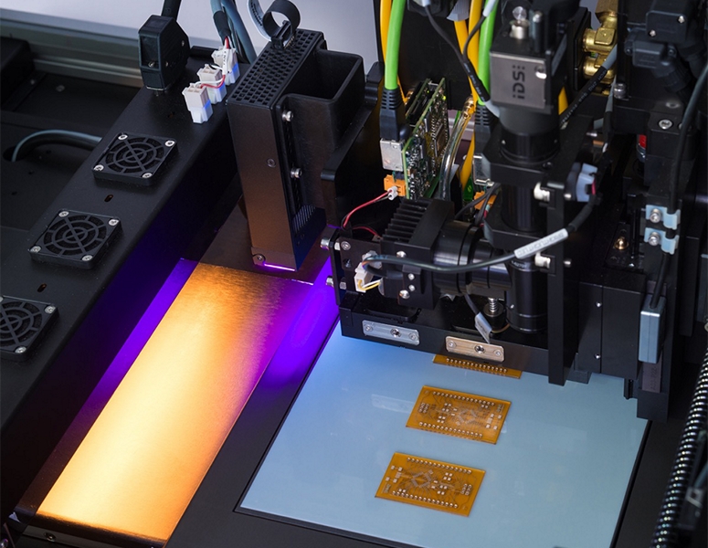
Several PCBs on the DragonFly 2020 Pro platform.
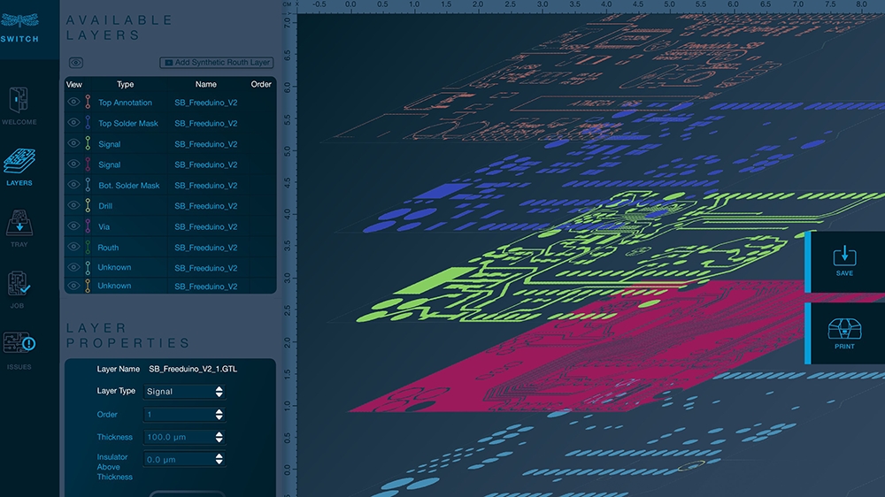
PCB production preparation for DragonFly 2020 Pro is carried out in the Switch software package.
Nano Dimension comes with a printer plug-in for SolidWorks.
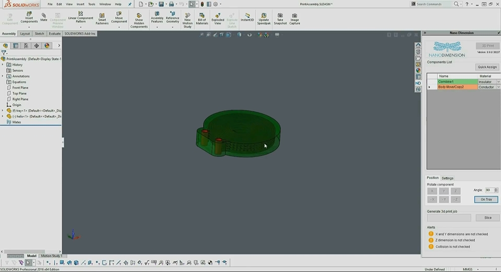
The plug-in for SolidWorks allows you to assign materials to different parts of the product, position the product inside the printer chamber, slice and start printing.
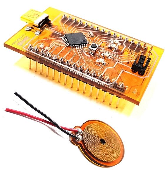
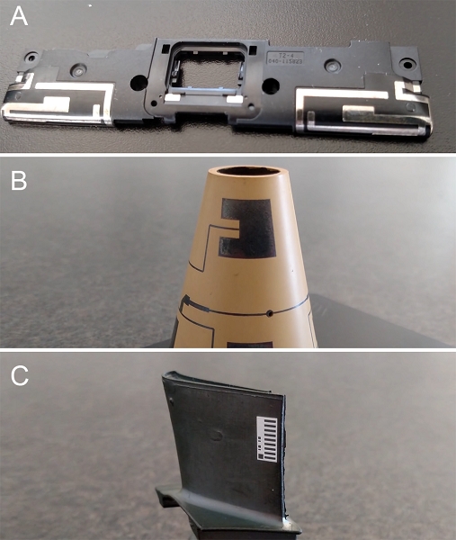
Examples of electronic devices manufactured using DragonFly 2020 Pro.
Another developer of professional 3D printers for electronics is Optomec (Optomec). For printing electronic components, the company offers aerosol application technology (Aerosol Jet). In printers using this technology, the ink first enters the atomizer chamber, where they are dispersed in a suspension of particles with a diameter of 1-5 microns. Then, with a flow of carrier gas, this aerosol is applied to the substrate. This method resembles the laser-deposition method (Directed Energy Deposition) used for printing metals.

Antenna printing using aerosol spraying.
Aerosol Jet technology allows you to print resistors, capacitors, antennas and thin-film transistors. The electronic characteristics of the components can be controlled by changing the print settings. The technology allows you to print on surfaces of different nature: plastic, ceramic and metal. After applying the ink is baked with light.
Optomec offers a whole range of professional 3D printers that incorporate Aerosol Jet technology. In some models of printers, this method is combined with a multi-axis substrate positioning system, so electronic components can be printed on the surface of almost any shape. For example, antennas can be printed directly on the cell phone. One of these models:
Optomec Aerosol Jet 5X
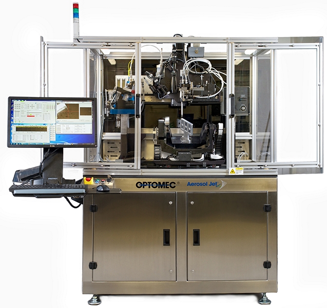
The appearance of the installation Aerosol Jet 5X.
Specifications
- Sizes of working area, mm: 200 × 300 × 200;
- Number of atomizers: 2 (ultrasonic and pneumatic);
- Positioning repeatability, micron: ± 2;
- Positioning accuracy, micron: ± 10 (per 100 mm)
- Support ink set with a wide range of viscosity;
- Module for UV curing ink;
- Layer thickness in one pass, micron, from: 0.1 - 6;
- Drop size, micron: 1-5;
- Minimum line width, µm: 10-20 (depending on materials);
- The ability to print biological materials;
- Conformal 3D printing (on surfaces of a complex profile).
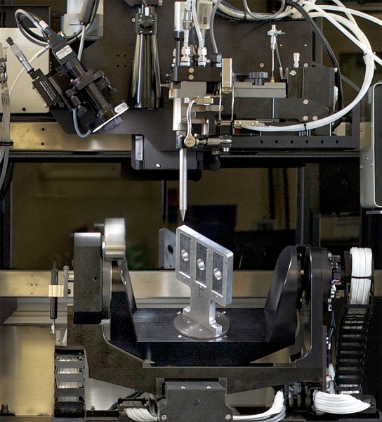
Working chamber Aerosol Jet 5X with metal billet installed.
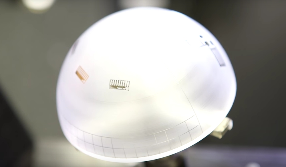
Electronic components printed on the surface of the hemisphere using
Aerosol Jet 5X.
Antennas and sensors printed with Aerosol Jet 5X on surfaces of complex topology.
3D printing of enclosures and mechanical accessories for electronic devices
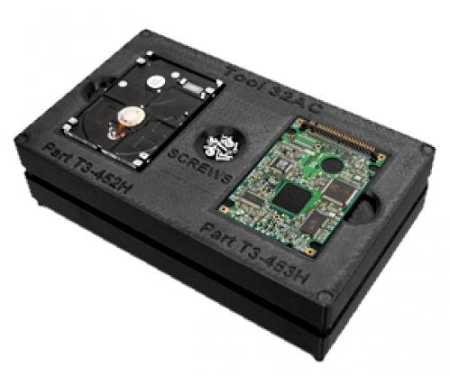
For the production of shells and mechanical equipment (for example, parts of actuating units: guides, gears, pulleys, etc.) for electronic devices, the classical methods of 3D printing are used: FDM, SLS, SLA.
For example, Gemecod (“Gemcod”) used 3D printing to produce parts for the mechanical components of the Ikilock electronic door lock: large parts that do not require high surface quality were made of polyamide, small parts with low surface roughness were manufactured using Polyjet. According to the developers, the use of 3D printing has accelerated product design optimization several times.
Mechanical parts of the electronic lock Ikilock, made by 3D-printing.
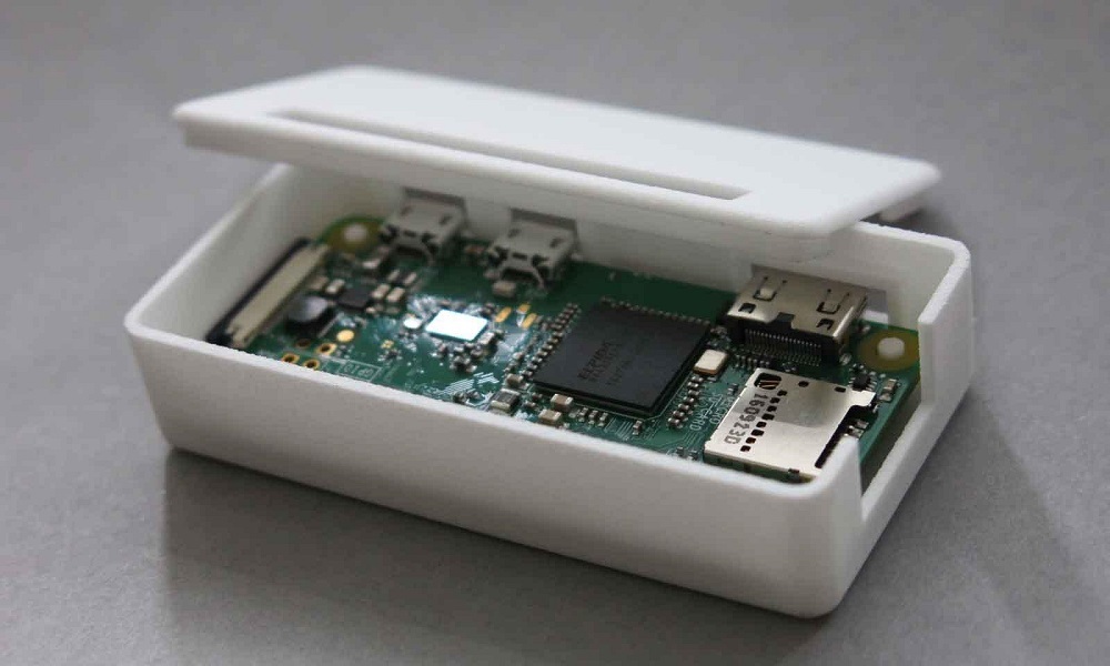
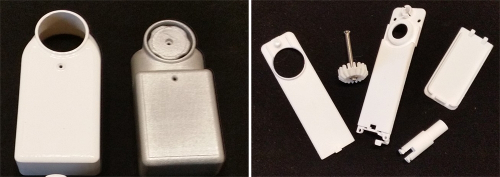
Electronic device housing made by the SLS method.
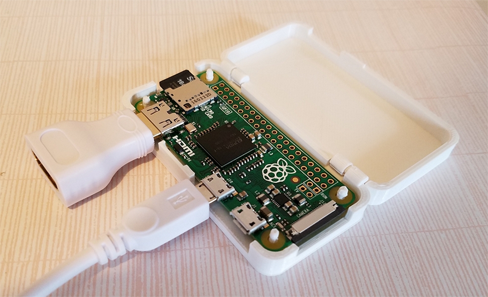
Electronic housing made by FDM.
An interesting direction is the use of 3D printing for the manufacture of unmanned aircraft fuselages. The material for this should be both light and durable. The Nano-racing company ("Nano-racing") uses such fuselages made by the SLS method for its drones.
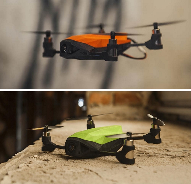
Drones Nano-racing with the fuselage, manufactured by 3D-printing.
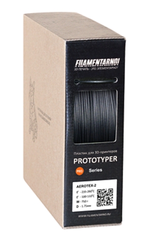
Printing drone fuselages can also be implemented using the FDM method. A good choice for this is Filamentarno! Pro Aerotex :
It should be noted that for the manufacture of electronic enclosures it is desirable to use materials with a reduced risk of electrostatic discharge (ESD-Safe). Many common materials for FDM printing have their own antistatic modifications : PLA, ABS, PETG; ESD-Safe engineering plastics: Ultem, PPS, PVDF, PC, POM.

Detail from Apium POM-C ESD with reduced risk of electrostatic discharge.
A good example is ABS-ESD7 Stratasys .
Detail of ABS-ESD7 Stratasys .
Conclusion
As we see from the above examples, 3D printing has already reached sufficient development to be used not only in the manufacture of cases and prototypes, but also full-featured electronic components. The devices mentioned in the article can be used both in development and prototyping, for creating prototypes, and for mass commercial production. Do not forget about the possibility of educational application.
The Voltera V-One compact personal printer is an excellent solution for quickly prototyping simple PCBs and optimizing them. V-One follows the classic planar paradigm and will be useful for any company engaged in the design or repair of electronics. Voltera V-One has great potential for use in schools and technical universities, as it allows you to quickly produce a prototype of the board and, thus, can be easily integrated into the educational process.
Voxel8 is a solution for creating electronic products at the same time as the body and the supporting structures. The use of PLA can limit the use of this printer in a number of tasks in which the operation of electronics is associated with a noticeable heat release, since this plastic does not have high heat resistance. Voxel8 can be an interesting option for 3D printing enthusiasts, makers and educational institutions. But its price, which is more likely to correspond to professional equipment, makes it more suitable for functional prototyping of products by developers.
Specialization of professional 3D-printers Nano Dimension - the production of prototypes of printed circuit boards of any complexity. The scope of Optomec installations is not limited to prototyping printed circuit boards: supporting a wide range of inks and substrate materials for printing, the ability to print on complex surfaces, and a modular design make these systems a flexible, universal solution for development, prototyping and electronics production.
Choose a 3D printer for printing electronics will help you in the Top 3D Shop .
Want more interesting news from the world of 3D technology?
Subscribe to us in the social. networks:


Source: https://habr.com/ru/post/424413/
All Articles