Silicon photonics stumbles at the last meter
We have already laid the optics to the house, but it is still problematic to lay it to the processor.
If it seems to you that today we are on the verge of a technological revolution, imagine what it was in the mid-1980s. Silicon chips used transistors with a characteristic size measured by microns. Fiber-optic systems moved trillions of bits around the world at tremendous speeds. It seemed that everything is possible - it is only necessary to combine digital silicon logic, optoelectronics and data transmission over optical fiber.
Engineers imagined how all these breakthrough technologies would continue to evolve and converge at the point at which photonics merges with electronics and gradually replaces it. Photonics would allow moving bits not only between countries, but also inside data centers, and even inside computers. Optical fiber would move data from chip to chip - so they thought. And even the chips themselves would be photonic - many believed that incredibly fast logic chips would someday begin to work using photons instead of electrons.
Naturally, this did not happen. Companies and governments have invested hundreds of millions of dollars in the development of new photon components and systems that integrate racks of computer servers in data centers using fiber. And today, such photon devices really connect the racks in many data centers. But the photons stop there. Inside the rack, the individual servers are connected to each other using inexpensive copper wires and high-speed electronics. And, of course, metal conductors are placed on the boards themselves, all the way up to the processor.
')
Attempts to push the technology into the servers themselves, directly feed the fiber optic processors, based on the economic foundation. Indeed, there is a market for optical transceivers for Ethernet with a volume of almost $ 4 billion a year, which should grow to $ 4.5 billion and 50 million components by 2020, says LightCounting, a market research company. But the photonics did not pass these last few meters separating the computer rack in the data center and the processor.
Nevertheless, the enormous potential of this technology continued to support the dream. While technical problems remain significant. But now, finally, new ideas about data center schemes offer feasible ways to organize the photon revolution, which can help contain the influx of big data.
Inside the photon module
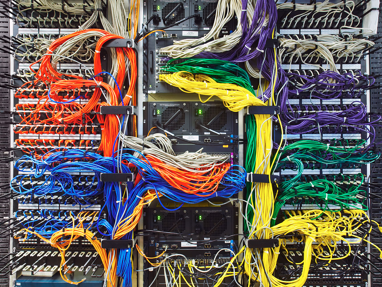
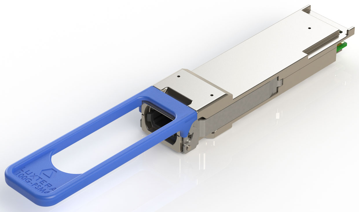
Every time you browse the web, watch digital TV, or perform virtually any action in today's digital world, you use data that has passed through optical transceiver modules. From the task - to convert the signal between the optical and digital modes. These devices live on each end of the optical fiber that drives the data inside the data center of any major cloud service or social network. Devices are included in the switch located at the top of the server rack and turn optical signals into electrical ones so that they can reach several servers in this rack. Transceivers also convert data from these servers into optical signals for transmission to other racks or via a whole network of switches to the Internet.
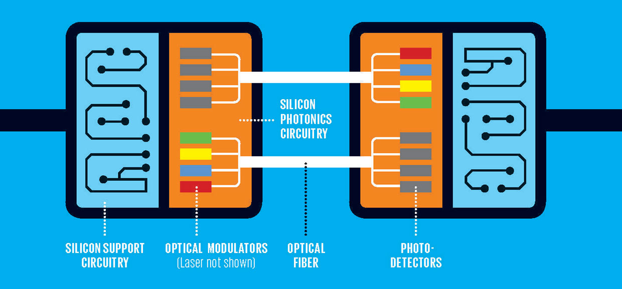
Each optical module contains three main components: a transmitter with one or several optical modulators, a receiver with one or several photodiodes, and CMOS chips encoding and decoding data. Ordinary silicon emits light very poorly, so the photons are generated by a laser separated from the chips (although it can be placed in the same case as them). The laser does not represent the bits by switching on and off - it is on all the time, and the bits are encoded in the beam of its light using an optical modulator.
This modulator, the heart of the transmitter, can be of various kinds. Especially successful and simple is called the modulator Mach-Zehnder. In it, a narrow silicon waveguide directs the laser light. The waveguide branches into two, and after a few millimeters, they converge again. In a typical situation, such a fork and connection would have no effect on the light output, since both arms of the waveguide have the same length. Connecting back, the light waves remain in phase with each other. However, if one voltage is applied to one branch, it will change its refractive index, which will slow down or speed up the light wave. As a result, after meeting two waves, they interfere with each other in a destructive way, suppressing the signal. Therefore, by varying the voltage on the branch, we use an electrical signal to modulate the optical.
The receiver is simpler: it's just a photodiode and its supporting circuits. The light passing through the fiber reaches a germanium or silicon-germanium photodiode of the receiver, which produces a current - usually each light pulse is converted into voltage.
The modulator and receiver are serviced by circuits involved in amplification, packet processing, error correction, buffering, and other tasks that need to be solved in order to meet the Gigabit Ethernet standard for optical fiber. How many tasks are performed on the same chip, or at least in the same package that controls photonics, depends on the manufacturer, but most of the electronic logic is separated from photonics.
Photonics can never transfer data between different parts of a silicon chip. The circular oscillator of an optical switch performs the same function as a single transistor, however, it takes up 10,000 times more area.
There are more and more silicon integrated circuits with optical components, and this may make you think that the integration of photonics into the processor was inevitable. And for some time it was thought so.
However, the growing discrepancy between the rapid decrease in the size of chips with electronic logic and the inability of photonics to keep up with them was underestimated or even ignored. Today, transistors have characteristic dimensions of several nanometers. At 7 nm CMOS technology, more than one hundred general-purpose logic transistors can be placed on each square micrometer. And we still do not mention the labyrinth of complex copper wires above them. In addition to having billions of transistors on each chip, there are a dozen more levels of metal connections connecting these transistors to registers, multipliers, arithmetic logic devices, and more complex designs that make up the processor cores and other necessary circuits.
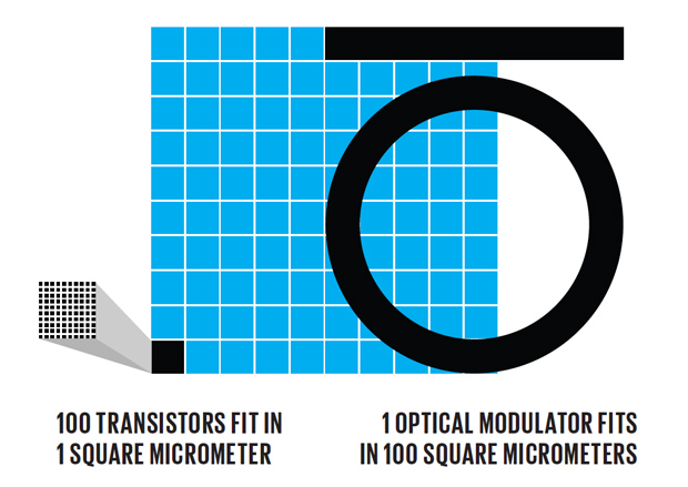
The problem is that a typical optical component, such as a modulator, cannot be made significantly smaller than the wavelength size of the light that it carries - which limits its minimum width to 1 micrometer. No Moore's law of this restriction will overcome. It is not a question of using more and more advanced lithography technologies. Just electrons - the wavelength of which is several nanometers - is thin, and photons are thick.
But can not manufacturers simply integrate the modulator and accept the fact that there will be fewer transistors on the chip? After all, are there already billions of them? Can not. Due to the huge number of system functions that each square micrometer of a silicon electronic chip is capable of performing, it will be very expensive to replace even not very many transistors with worse-performing optical-type components.
Simple counting. For example, an average of 100 transistors is located on a square micrometer. Then an optical modulator occupying an area of 10 µm by 10 µm replaces a circuit consisting of 10,000 transistors! Recall that a conventional optical modulator operates as a single switch that turns the light on and off. But each transistor itself can work as a switch. Therefore, roughly speaking, the cost of including this primitive function in the circuit is 10,000: 1, since each optical modulator has 10,000 electronic switches that the circuit designer can use. No manufacturer will accept such a high cost, even in exchange for a perceptible increase in speed and efficiency that could be obtained from integrating modulators directly into the processor.
The idea of replacing electronics with photonics on chips has other disadvantages. For example, on a chip, critical tasks are performed, like working with memory, for which optics have no opportunities. Photons are simply incompatible with the basic functions of a computer chip. And in cases where this is not the case, it does not make sense to arrange a competition between optical and electronic components on the same chip.
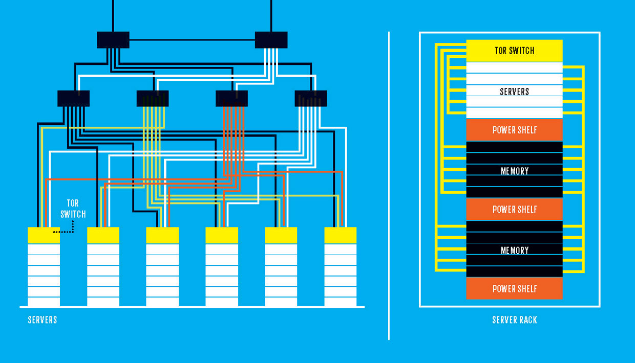
The scheme of the data center.
Today (left) photonics transmits data over a multi-tier network. Internet connection is at the top (main) level. The switch transmits data over fiber to the top rack switches.
Tomorrow (on the right) photonics can change the architecture of data centers. Rack scale architecture could make data centers more flexible by physically separating computers from memory and linking these resources across an optical network.
But this does not mean that optics will not be able to get close to processors, memory and other key chips. Today, the optical communications market in data centers revolves around top-of-rack (TOR) switches, which include optical modules. At the top of two-meter racks in which servers, memory and other resources are installed, optical fiber links the TORs together using a separate layer of switches. And they are connected to another set of switches that form the output of the data center to the Internet.
A typical TOR panel where transceivers are plugged in gives an idea of data movement. Each TOR is connected to one transceiver, and that, in turn, is connected to two optical cables (one per transmission, the second per reception). In the 45 mm high TOR, you can plug in 32 modules, each of which is capable of transmitting data at a speed of 40 Gbit / s in both directions, with the result that data can be transmitted at a speed of 2.56 Tbit / s between two racks.
However, within the racks and inside the servers, data still flows through the copper wires. This is bad, as they become an obstacle to the creation of faster and more energy-efficient systems. Optical solutions of the last meter (or a couple of meters) —the connection of the optics to the server or even directly to the processor — are probably the best opportunity to create a huge market for optical components. But until then it is necessary to overcome serious obstacles both in the field of prices and in the field of speed.
Circuits called "fiber to processor" are not new. The past gives us a lot of lessons about their cost, reliability, energy efficiency and channel width. About 15 years ago, I participated in the development and creation of an experimental transceiver , which demonstrated a very high throughput. The demonstration connected a cable of 12 optical wires to the processor. Each core transmitted digital signals generated separately by four vertical-resonator surface-emitting lasers (VCSEL). This is a laser diode, emitting light from the surface of the chip, and the light has a higher density than conventional laser diodes. Four VCSELs coded the bits by turning the light on and off, and each of them worked at its frequency in the same core, which increased its transmission capacity fourfold due to the coarse spectral bandwidth of the channels . Therefore, if each VCSEL produced a data stream of 25 Gbit / s, then the total system throughput reached 1.2 Tbit / s. Today, the industry standard distance between adjacent conductors in a 12-core cable is 0.25 mm, which gives a throughput density of 0.4 Tbit / s / mm. In other words, in 100 seconds each millimeter can process as much data as the web archive of the Library of Congress of the USA saves in a month.
Today, even higher speeds are required to transfer data from the optics to the processor, but the beginning was quite good. Why is this technology not accepted? Partly because this system was both insufficiently reliable and impractical. At that time it was very difficult to make 48 VCSEL for the transmitter and to guarantee the absence of failures during its lifetime. An important lesson is that a single laser with many modulators can be made much more reliable than 48 lasers.
Today, VCSEL reliability has increased so much that transceivers using this technology can be used in solutions for short distances in data centers. Optical conductors can be replaced with multi-core optics, carrying as much data, redirecting them to different threads inside the main fiber. Also recently, it has become possible to implement more sophisticated digital data transmission standards - for example, PAM4 , which increases the data transfer speed using not two, but four light powers. Research is being conducted in the direction of increasing the bandwidth density in data transmission systems from optics to the processor — for example, the MIT Shine program makes it possible to achieve 17 times more density than was available to us 15 years ago.
All these are quite significant breakthroughs, but taken together, they will not be enough to allow photonics to take the next step towards the processor. However, I still believe that such a move is possible - because now the movement to change the system architecture of data centers is gaining momentum.
Today, processors, memory and storage system are collected in the so-called. blade servers whose special enclosures are located in racks. But this is not necessary. Instead of placing the memory on the chips in the server, it can be placed separately - on the same, or even on a different rack. It is believed that such a rack-scale architecture ( rack-scale architecture , RSA) can more efficiently use computational resources, especially for social networks like Facebook, where the amount of computation and memory needed to solve problems grows with time. It also simplifies the maintenance and replacement of equipment.
Why does such a configuration help photonics to penetrate deeper? Because it is precisely this ease of configuration change and dynamic resource allocation that you can afford thanks to a new generation of efficient, low-cost optical switches that transmit several terabits per second.
The technology of connecting optics directly to the processor has existed for over 10 years
The main obstacle to this change in data centers is the cost of components and their production. Silicon photonics already have one cost advantage - it can take advantage of existing production facilities, a huge chip production infrastructure and its reliability. However, silicon and light combine imperfectly: in addition to interfering inefficiency in the emission of light, silicon components suffer from large light losses. A typical silicon optical transceiver shows optical loss of 10 dB (90%). This inefficiency does not matter for short connections between TOR switches, as long as the potential cost advantage of silicon outweighs its disadvantages.
An important part of the cost of a silicon optical module is such a modest but crucial detail as an optical connection. This is the physical connection of the optical fiber and the receiver or transmitter, and the connection between the fibers. Every year, hundreds of millions of optical and optical connectors have to be manufactured with the highest precision. To imagine this accuracy, note that the diameter of a human hair is usually only slightly smaller than the diameter of a single strand of 125 μm fiber used to connect optical cables. The accuracy with which it is necessary to align the fiber in the connector is about 100 nm - one thousandth of the thickness of a human hair - or the signal will attenuate too much. It is necessary to develop innovative methods for the production of connectors for two cables and for connecting the cable to the transceiver in order to meet the growing customer demands for high accuracy and low cost. However, there are very few production technologies that make production quite inexpensive.
One way to reduce the cost is to reduce the cost of the optical module chips. Here the technology of implementing systems at the level of the whole substrate ( wafer-scale integration , WSI) can help. According to this technology, photonics are placed on one silicon substrate, electronics - on the other, and then the substrates are connected (a laser manufactured not from silicon, but from another semiconductor, remains separate). This approach saves the cost of production, since it allows for parallel production and assembly.
Another factor reducing the cost is, of course, the volume of production. Suppose that the entire market for optical Gigabit Ethernet is 50 million transceivers per year, and each chip of an optical transceiver occupies 25 mm square. Assuming that the factory uses for its production substrates with a diameter of 200 mm, and that then 100% of the output is used, this market requires 42,000 substrates.
, . 25% . , . – , TOR, .
- , , . . , , .
, , , . , . , , .
15 . , -. . . . ? I think no.
Source: https://habr.com/ru/post/423911/
All Articles