Tips for using the HyperLynx DDR Wizard to analyze QDR4
Quad Data Rate (QDR-IV) is the standard for high-performance memory for networking applications and is ideal for the new generation of networking devices, communications equipment and computing systems.
QDR-IV SRAM has an integrated Error Detection and Correction Block (ECC) to ensure data integrity. This unit is able to handle all one-bit memory errors, including those caused by cosmic rays and alpha particles. As a result, memory modules will have a program error rate (SER) of no more than 0.01 failure / MB. QDR-IV is equipped with a programmable address parity function that ensures data integrity on the address bus.
')
Distinctive features of QDR SRAM memory:
- Built-in error correction module ensures data integrity and eliminates software errors
- The modules are available in two versions: QDR-IV HP (data transfer rate 1334 Mtrans / s) and QDR-IV XP (data transfer rate 2132 Mtrans / s)
- Two independent bidirectional DDR1 memory data ports
- Bus inversion function to reduce noise while simultaneously connecting input and output lines
- Built-in matching circuit (ODT) reduces board complexity
- Skewed training to improve signal acquisition timing
- I / O signal level: 1.2V to 1.25V (high-speed transceiver logic (HSTL) / terminated logic (SSTL)), 1.1V to 1.2V (POD2)
- 361-pin FCBGA3 package
- Bus width: x18, x36 bits
Introduction
DDRx Wizard is an easy-to-use tool in HyperLynx that allows you to monitor time waveforms in batch mode and analyze the signal integrity of standard DDR JEDEC protocols. The DDRx Wizard can be launched both at the stage of the pre-topological analysis according to the “what if” scenario, and on a fully traced board. In addition, the tool allows you to import most of the formats of the models created by major suppliers of microcircuits.
DDRx Wizard allows you to check all the bits of the memory bus for compliance with the integrity of the signal, as well as for compliance with the requirements of synchronization between signals. This article will detail the use of an interactive assistant to analyze projects implementing the QDR4 protocol (Figure 1).
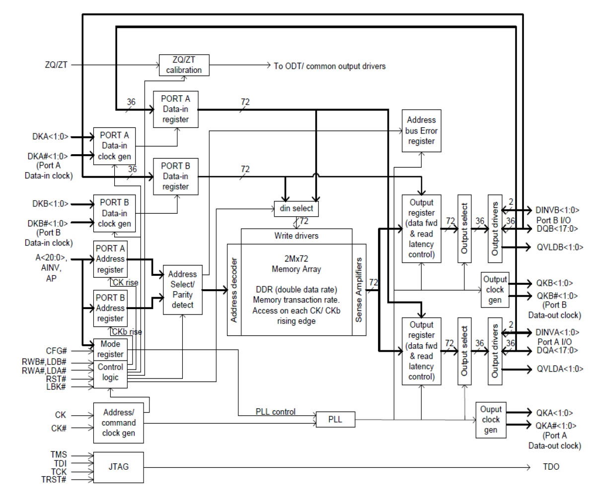
Fig. 1. Internal QDR architecture using the example of the CY7C4142KV13 module (clickable)
First look at QDR-IV in HyperLynx DDRx WIZARD
The QDR-IV protocol defines two unidirectional pairs of a data strobe signal: one for reading data, the other for writing, which support independent operation and simultaneous read and write operations, and the ports can operate at different frequencies (Fig. 2). Thus, the risk of malfunction is completely excluded.
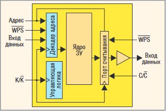
Fig. 2. Availability of separate ports for reading and writing in the QDR SRAM architecture
For this protocol, the DDRx Wizard will use separate gates for read and write operations. QDR IV is usually implemented using an x36 or x18 bit bus (see Figure 3a and 3b).
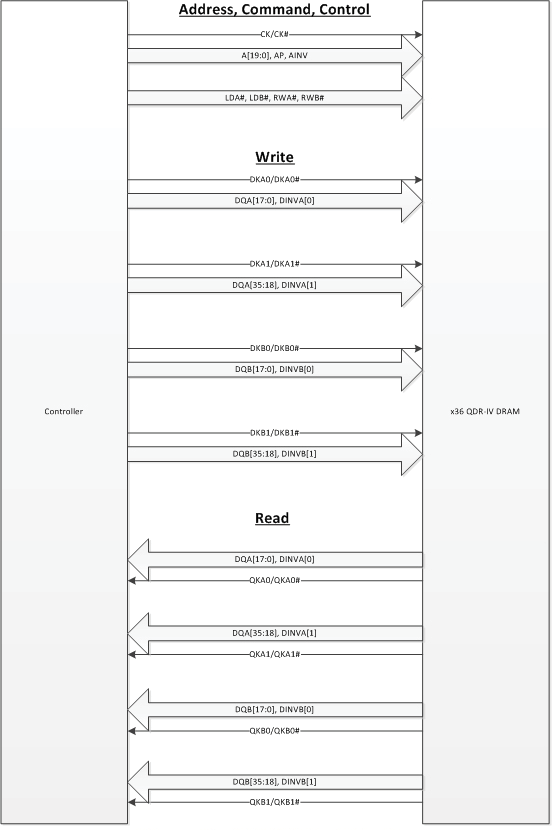 Fig. 3a QDR- IV, x36-bit Fig. 3a QDR- IV, x36-bit | 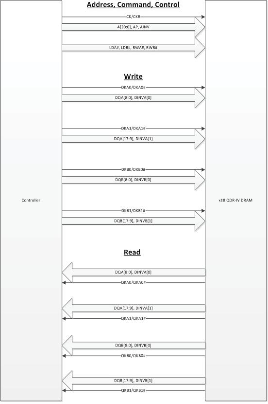 Fig. 3b. QDR- IV, x36-bit Fig. 3b. QDR- IV, x36-bit |
DDRx Wizard allows you to simulate QDR-IV in three stages:
- Check reading data
- Validation of data records
- Check address / control bus
Since the address / control bus can be checked independently of data read / write checks, this can save you time by combining this step with any of the data testing steps. The following describes all three test data scenarios.
Technological features
QDR-IV supports pseudo open drain technology (POD) and Stub Series Terminated Logic (SSTL) terminating logic (Figure 4).
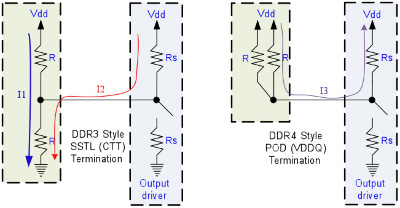
Fig. 4. Differences between POD and SSTL
Regardless of the logic standard used, select LPDDR3 as the technology (Fig. 5), since there is no support for Vref training , as is the case with the DDR4's POD module. Instead, it uses fixed Vref and Vinh / Vinl values, similar to DDR3 and LPDDR3. Since QDR-IV uses double data rates for address signals like LPDDR3, it is recommended to select this option. Next, enter the transfer rate of user data, for example, 1866 MT / s or 2133 MT / s, where MT / s is the number of megatransactions per second (megatransfers per second).
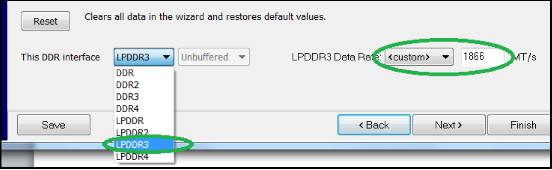
Fig. 5. Choice of logic standard
Data signal: read operation
For data read operations, the DRAM will control the DQ signals in conjunction with the differential gates QK signals. Thus, the setting focuses on the data read operation, and assigns the necessary circuits (signals) to the corresponding QK gate.
In the Nets to Simulate section (Fig. 6), tick the box “ Read Cycles Only ” ( Read Cycles Only ). Checkboxes Clock-to-strobe and Address checks are optional.
Also, check the installation of the checkbox Compensate signal launching skews .
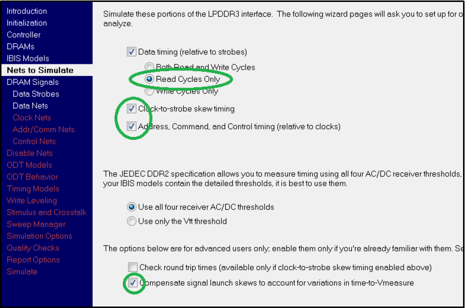
Fig. 6. Reading data
Make sure that all necessary data gates are selected (Fig. 7).
In the Data Nets section, verify that the signals match each strobe. Please note that for x18 and x36 bit buses, the signals are different, so make sure that the pinout is correct for your particular case (Fig. 8a and 8b).
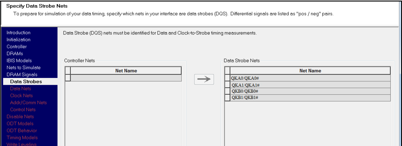
Fig. 7. Reading Data Strobe
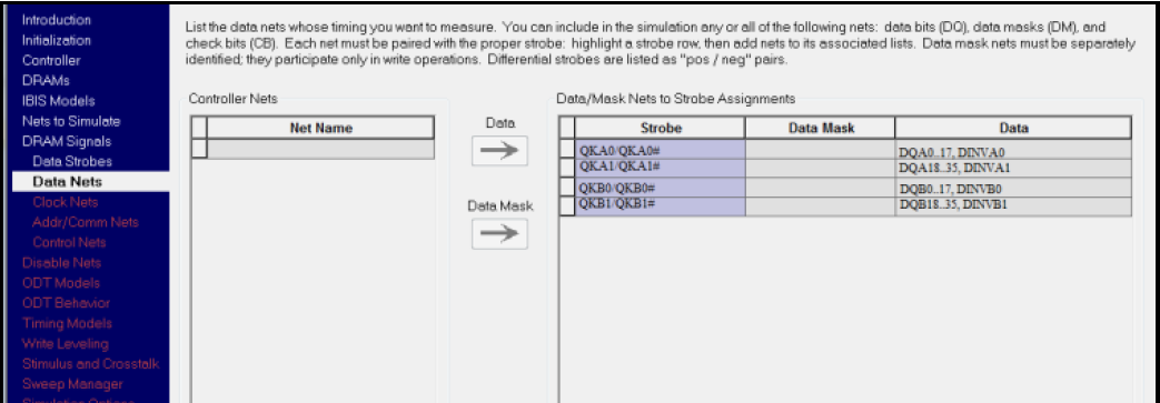
Fig. 8a. Signal group for 36-bit bus
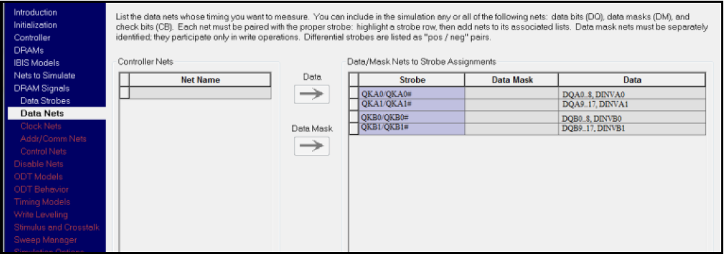
Fig. 8b. Signal group for 18-bit bus
Parallel bus checks are usually performed by setting / delaying the time between the strobe and the signal. All these requirements, in addition to other time values, are needed by the DDRx Wizard to verify the results. These values may differ from chip to chip, so it is recommended to enter values that apply to a specific memory device. In addition, the default timing information for LPDDR3 is incompatible with QDR-IV. So, all the timing information for QDR-IV should be entered and correspond to the documentation for your chip.
This can be done either with the help of the Timing Wizard (Fig. 9), which prompts the user to fill in several forms for the subsequent generation of time values, or you can edit the .V synchronization files corresponding to your controller and DRAM.
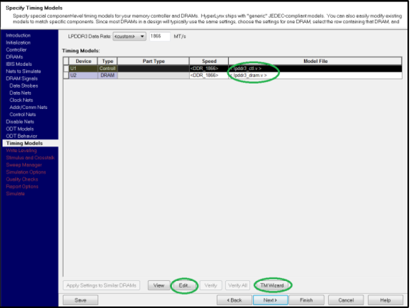
Fig. 9. Setting Timing Values
Please note : since the simulation is performed in the LPDDR3 mode, the results should be interpreted accordingly.
Data signal: write operation
The data writing operation and its analysis is similar to the analysis for the read operation described above. But there are two key differences that we will now consider. With the exception of these two nuances, the steps performed for a data read operation can be repeated to simulate data writing.
In the Nets to Simulate section (Figure 10), make sure that the Write Cycles Only option is selected.
It is also possible to simulate the operation of writing the address signal ( Address Signal write Operations ). And don't forget to make sure that the Compensate Skew Launch checkbox is checked .
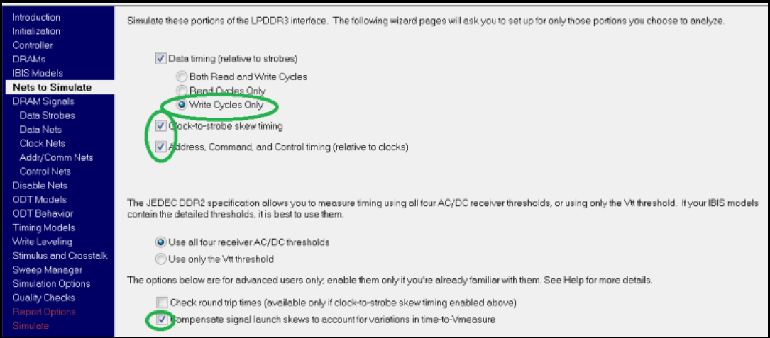
Fig. 10. Record data
Make sure that the correct gates are selected in the Data Strobe section (Figure 11). The key difference between a read transaction and a write transaction is the strobe used for data synchronization, this strobe is different from the strobe used for the data read operation (Fig. 12 and 13).
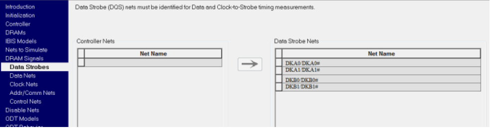
Fig. 11. Record data gates
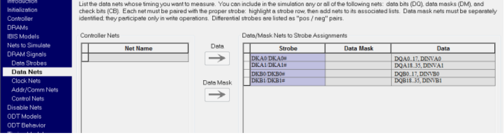
Fig. 12. Signal strobe signal groups (36-bit bus)

Fig. 13. Signal strobe signal groups (18-bit bus)
Bus address, commands and controls
QDR-IV uses CK / CK # differential clocks to select control signals, addresses, and command signals. The leading edge of the CK signal is used to enter information about port A, and the back is to select information about port B.
Taking into account the integrity of the signal, the waveforms for the address lines must meet the installation requirements and delays of both the leading and trailing edges of the clock signal. This is very similar to the behavior of LPDDR3.
LDA #, LDB #, RWA # and RWB # signals are synchronized with a single data rate (single-data-rate). This means that these signals are synchronized only on one of the two clock edges. The LDA # and RWA # signals are synchronized on the rising edge of the clock, and the LDB # and RWB # signals - on the falling front.
The blocks are largely symmetrical - the front differential front is not much different from the rear. This means that to ensure the integrity of the signals, the timing values for LDB # and RWB # should be almost the same, if not identical when sampling at the leading or trailing edge of the clock signal. LPDDR3 control signals are also synchronized on the leading edge only.
The following steps are specific to simulating address buses, commands, and controls when using QDR-IV.
Make sure that Address, Command and Control timing (relative to clocks) is checked in the Nets to Simulate section (Fig. 14).
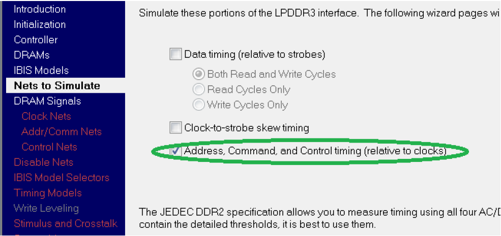
Fig. 14. Set the Address, Command and Control timing checkbox.
In the Clock Nets section, make sure that the differential pair of CK / CK # clock signals is selected (Figure 15).
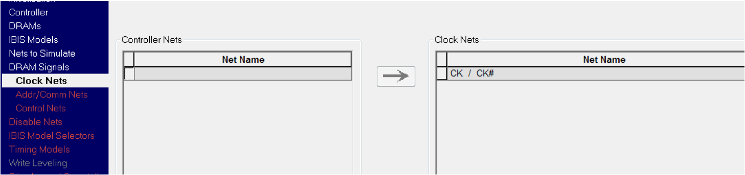
Fig. 15. Selection of differential sync
In the Addr / Comm Nets section, make sure that bits A [20: 0] are selected for devices with x36 and bits A [19: 0] are for devices with x18. In addition, set the signals AP and AINV (Fig. 16 and 17).
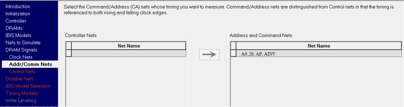
Fig. 16. Settings for x36-bit tires
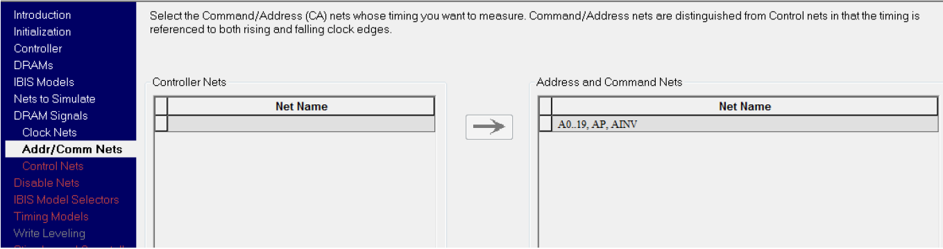
Fig. 17. Settings for x18-bit tires
In the Control Nets section, select the LDA #, LDB #, RWA #, and RWB # signals (Figure 18).
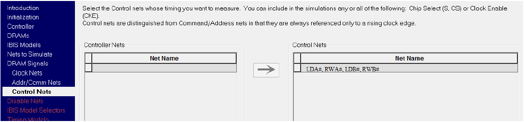
Fig. 18. Control signals
As in the case of modeling the data signal, make sure that you use the correct files with the timing parameters. The rest of the simulation and evaluation results are similar to LPDDR3.
“Interpreting the results of the HyperLynx DDRx report”
Conclusion
By following the simple instructions provided in this article, you can benefit from and effectively use the DDRx Wizard helper package to simulate and test QDR-IV tires.
I hope this manual will be useful to someone.
Sincerely, Filipov Bogdan ( pbo ).
I also take this opportunity to invite the developers of REI to a seminar organized by Nanosoft and Mentor Graphics:
"A new generation of solutions for the design of electronic devices from Mentor Graphics"

Source: https://habr.com/ru/post/423897/
All Articles