Introducing the World of Counterfeit ICs: Counterfeit Detection Techniques
Article published on December 23, 2017
The best option in the production of electronics - when all the components are original from the manufacturer, but what if you have a second-hand microcontroller that will not live long? If the transistor in the input voltage protection circuit does not match the parameters from the specification? Then your product will have serious problems. The microcontroller can fail, and the circuit can not cope with the load.
In fact, it is not your fault or design error. The reason - in fake chips. You can say: "The microcontroller chip is correctly labeled and looks like the original - this is exactly the original." And I will answer: are you sure that the right crystal is inside ?!
')
On fakes you can earn money. A counterfeit market study states that some firms earn $ 2 million a month by selling just one type of counterfeit component.
When a distributor does not have a specific component in stock, sometimes manufacturers and developers have to deal with brokers and third-party suppliers. This happens if the item is needed urgently or at a lower price. Be that as it may, they may become victims of the purchase of fake chips that are distributed in different ways. Defects begin to appear with small failures, and ends with a complete failure.
The use of fakes is a big risk. And often they go unnoticed until all components are assembled into a printed circuit board. The subsequent alteration will cost much and take a lot of time.
This is a growing threat in the global market. In November 2011, the US Senate Committee on Armed Forces held hearings in connection with an increase in the number of fake components in the US military supply chain. The committee initiated an audit of contractors of the Ministry of Defense .
Moreover, as a result of the use of counterfeit microelectronics, serious disasters can occur. Here are examples of some incidents mentioned in the report of the Association of the semiconductor industry SIA :
So yes. This is a serious global threat.
Many reports and studies estimate the scale of counterfeit. In the report of the International Chamber of Commerce from 2008, the annual market volume in the G-20 countries was estimated at $ 775 billion with an increase to $ 1.7 trillion in 2015 .

Fig. 1. Number of reported incidents with counterfeit components reported by IHS, source
Another study conducted by the US Department of Commerce from 2005 to 2008 showed that 50% of component manufacturers and 55% of distributors encountered counterfeit components.
Moreover, experts estimated that among all Pentagon's purchases of spare and replacement components, up to 15% are counterfeit products.
Hackers, intellectual property hijackers and counterfeiters always adapt quickly and find new methods. In this article, we mention the most common methods of manufacturing fakes.
Experts usually divide methods into categories:
I would like to analyze the second classification in more detail.
As a starting point, let's take a classification from this work and improve it.
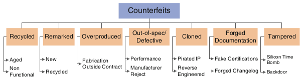
Fig. 2. Taxation of fakes, source
This is the most common way to fake. Over 80% of the counterfeit components were recycled and remarked . During recycling, components are removed from recycled printed circuit boards, their enclosures are repainted and / or remarked, and then they are sold as new parts.
In some cases, the crystal is removed from the case, then mounted in a new case and remarked for the desired device. Here the most dangerous, if the component is not functional or was damaged during previous use.
Extraction of the crystal includes acid decapsulation of the plastic body, extraction of wire joints (which connect the crystal with external pins) using tweezers, heating of the body and grinding the back side. Then the crystals are sent to China for assembly in new buildings.

Fig. 3. Removing the crystal from the shell, the source
New wire connections are clear evidence of crystal reuse when a new mount is in place of the old one.
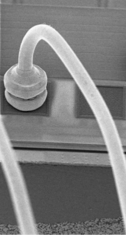
Fig. 4. New wire connection at the old contact, source
The objectives of remarking may be as follows:

Fig. 5. AMD processor with Intel chip, source
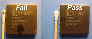
Fig. 6. Test Dynasolve on two Xilinx chips, source

Fig. 7. Examples of chips after processing and remarking, source
Cloned components are produced by unauthorized manufacturers without legal rights to produce the chip. The original design is cloned using reverse engineering.
Falsified components may include “hardware trojans” and may merge valuable information to the manufacturer. In fact, reverse engineering and the introduction of hardware Trojans is a separate broad topic for another article.
If you want to protect your home or office, the first thing you need to do is change your thinking style: think not as a guard, but as a thief. The first step to defending against fake ICs is to learn the methods of the enemy.
The second step is to look for clues.
Defects seem innumerable. The proposed taxonomy of defects shows the overall picture.
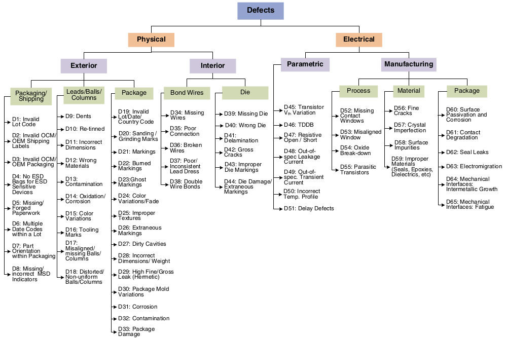
Fig. 8. Taxonomy of counterfeit component defects, source
Some defects are easier to detect than others. By the way, some of them are easiest to detect with the naked eye.

Fig. 9. Two fake Tundra bridges from PCI to Motorola, source
These two integrated circuits are repainted and remarked, but the circled fragment is clearly shifted.

Fig. 10. Repainted Circuits, Source
The picture left clear traces of repainting.
Fig. 11. Holes from burning markings, source
Marking the body is a laser. Excess laser can burn through the case.
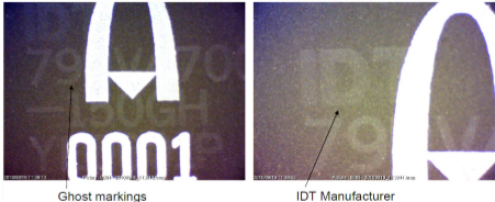
Fig. 12. Traces of old marking, source
Fig. 13. Picture CADBlog
The fake integrated circuit may not have the intended connections. They may disappear when repacking the crystal. An x-ray is used to detect this defect.
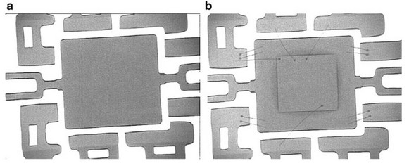
Fig. 14. Absence of connections, source
Another variant of internal defects is the use of a completely wrong crystal. For example, the American company Sparkfun found a supply of fake Atmega328 microcontrollers. The study revealed that they have the marking and body Atmega328, but the crystal inside does not even closely match the original microcontroller!
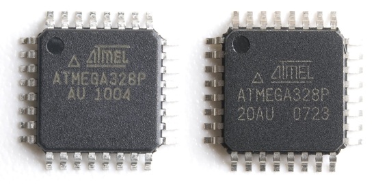
Fig. 15. On the left is the original Atmega328, on the right is a fake one. Sparkfun image

Fig. 16. Test of electrical parameters of a high-performance operational amplifier (fake and real), source
The counterfeit operational amplifier passed the test at 10-fold speed, and only the complex test with alternating current revealed a fake.
The proverb says that it is better to spend a penny on prevention than the ruble on treatment.
Detection of counterfeit components is a difficult task due to cost, testing time, lack of parameters to evaluate (sometimes) and quickly change technical methods of counterfeiting.
There are many mechanisms, each of which targets some of the fake methods and component types, as described in the following table:

Fig. 17. Methods of combating counterfeit, source
Let us consider some of these methods in more detail.
As the name of the sensor CDIR (Combating Die and IC Recycling), it is a method of dealing with the reuse of integrated circuits.
As a CDIR sensor, you can use different structures on a chip, but for the sake of simplicity, we mention only one of them: a sensor based on a ring oscillator (RO). Other structures see here .
This sensor captures every turn on the chip and makes it easy to check the data. It is composed of two ring generators: the RO sample and the RO under load. The principle is based on the fact that the effect of aging MOSFET changes the frequency of the RO. From the difference between the frequency of the RO sample and the RO under load, you can calculate the approximate chip usage time.
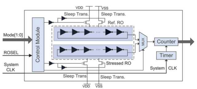
Fig. 18. RO-sensor circuit, source
As already mentioned in the chapter on counterfeit production methods, some developers give the production to an outside contractor. Sometimes it can produce an extra amount of original design chips without the knowledge of the owner of the intellectual property or even sell the design. To prevent this, the production process can be protected by cryptographic methods, that is, blocking individual hardware components of the chip with their owner unlocking the intellectual property during or after the test. The interaction of the owner of the intellectual property with the factory and the assembly line using the SST method is shown in the following diagram:

Fig. 19. Interactions between the owner of the intellectual property, the manufacturer and the assembly line, source
First, the owner of the intellectual property receives a random number (TRN) from the factory, generates a test key (TKEY) using the secret key and sends it to the factory for each crystal. There from TKEY using the public key is created by a modified TRN, which is used for testing. The owner receives the test results and can either refuse the batch or transfer TKEY to the assembly line for the manufacture of microchips if the test results are positive.
The assembly shop receives a TRN from the owner of the intellectual property and, after mounting the crystal in the case, again carries out tests. Then sends the answer to the owner of the intellectual property. That unlocks good chips using the final key (FKEY) - and sends them to the market.
This mechanism is part of the broader Package ID technology. It covers the following examples:
In the case of DNA labeling, molecules with a unique DNA sequence are mixed into the ink for labeling. To verify the authenticity of the chips, ink samples are sent to the lab. The technology requires maintaining a database of valid sequences.

A physical random function or a physically non-cloning function (PUF) is a function with a random result associated with the physical characteristics of the device. It is random and unpredictable, but repeatable under the same conditions. Since during the production process uncontrolled and unpredictable changes are made, no two chips are identical, but a silicon PUF with a unique identifier can be embedded in the chip.
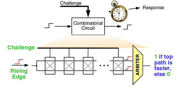
Fig. 20, adapted from source
The PUF measures the response for specific input data. Many methods are used to get the question-answer pair. One of them is the PUF delay, as shown in Fig. 20. Random changes in delays at contacts and gates of a crystal give random results. Arbitrator usually acts shutter, which gives 1 or 0, depending on which input came first. The PUF can support a huge number of question-answer pairs, where the answer is unique to each integrated circuit. Authentication operations require a trusted database of question-answer pairs.
Introduction
The best option in the production of electronics - when all the components are original from the manufacturer, but what if you have a second-hand microcontroller that will not live long? If the transistor in the input voltage protection circuit does not match the parameters from the specification? Then your product will have serious problems. The microcontroller can fail, and the circuit can not cope with the load.
In fact, it is not your fault or design error. The reason - in fake chips. You can say: "The microcontroller chip is correctly labeled and looks like the original - this is exactly the original." And I will answer: are you sure that the right crystal is inside ?!
')
On fakes you can earn money. A counterfeit market study states that some firms earn $ 2 million a month by selling just one type of counterfeit component.
Problem
When a distributor does not have a specific component in stock, sometimes manufacturers and developers have to deal with brokers and third-party suppliers. This happens if the item is needed urgently or at a lower price. Be that as it may, they may become victims of the purchase of fake chips that are distributed in different ways. Defects begin to appear with small failures, and ends with a complete failure.
The use of fakes is a big risk. And often they go unnoticed until all components are assembled into a printed circuit board. The subsequent alteration will cost much and take a lot of time.
Is this a serious problem?
This is a growing threat in the global market. In November 2011, the US Senate Committee on Armed Forces held hearings in connection with an increase in the number of fake components in the US military supply chain. The committee initiated an audit of contractors of the Ministry of Defense .
Moreover, as a result of the use of counterfeit microelectronics, serious disasters can occur. Here are examples of some incidents mentioned in the report of the Association of the semiconductor industry SIA :
- The broker has shipped fake microcontrollers for brake systems of European high-speed trains.
- The intermediary has shipped fake semiconductor components for use in nuclear submarines.
So yes. This is a serious global threat.
Problem in numbers
Many reports and studies estimate the scale of counterfeit. In the report of the International Chamber of Commerce from 2008, the annual market volume in the G-20 countries was estimated at $ 775 billion with an increase to $ 1.7 trillion in 2015 .
Fig. 1. Number of reported incidents with counterfeit components reported by IHS, source
Another study conducted by the US Department of Commerce from 2005 to 2008 showed that 50% of component manufacturers and 55% of distributors encountered counterfeit components.
Moreover, experts estimated that among all Pentagon's purchases of spare and replacement components, up to 15% are counterfeit products.
Fake methods
Hackers, intellectual property hijackers and counterfeiters always adapt quickly and find new methods. In this article, we mention the most common methods of manufacturing fakes.
Experts usually divide methods into categories:
- New components with incorrect marking and old components that are sold as new. [one]
- Functional and non-functional counterfeit. [2]
I would like to analyze the second classification in more detail.
As a starting point, let's take a classification from this work and improve it.
Fig. 2. Taxation of fakes, source
Remarking and Recycling
This is the most common way to fake. Over 80% of the counterfeit components were recycled and remarked . During recycling, components are removed from recycled printed circuit boards, their enclosures are repainted and / or remarked, and then they are sold as new parts.
In some cases, the crystal is removed from the case, then mounted in a new case and remarked for the desired device. Here the most dangerous, if the component is not functional or was damaged during previous use.
Extraction of the crystal includes acid decapsulation of the plastic body, extraction of wire joints (which connect the crystal with external pins) using tweezers, heating of the body and grinding the back side. Then the crystals are sent to China for assembly in new buildings.
Fig. 3. Removing the crystal from the shell, the source
New wire connections are clear evidence of crystal reuse when a new mount is in place of the old one.
Fig. 4. New wire connection at the old contact, source
The objectives of remarking may be as follows:
- Update date: old dates put the current date.
- Upgrading: changing the labeling to the upper class (military or industrial level components).
- Killing of failed components: some parts are already marked by the manufacturer as failed. They did not pass internal tests and were written off, but they could be taken out of the trash or smuggled.
Recycling and Remarking Examples
Fig. 5. AMD processor with Intel chip, source
Fig. 6. Test Dynasolve on two Xilinx chips, source
Fig. 7. Examples of chips after processing and remarking, source
Cloning and interference
Cloned components are produced by unauthorized manufacturers without legal rights to produce the chip. The original design is cloned using reverse engineering.
Falsified components may include “hardware trojans” and may merge valuable information to the manufacturer. In fact, reverse engineering and the introduction of hardware Trojans is a separate broad topic for another article.
Other fakes
- Lack of crystal inside. The manufacturer simply puts the desired labeling on the empty case. It is easy to detect by x-ray.
- Some designers order the production of chips for their design. Sometimes an unreliable contractor produces an extra batch of original microchips without notifying the customer. This is dangerous because the crystal and the case look exactly like the original, while counterfeit chips could not pass the tests provided by the customer before being delivered to the market.
- Fake documents. No physical forgery in the chips, but the attacker adds / changes some details in the documents. These may be fake specifications or electrical specifications.
Counterfeit Detection Techniques
If you want to protect your home or office, the first thing you need to do is change your thinking style: think not as a guard, but as a thief. The first step to defending against fake ICs is to learn the methods of the enemy.
The second step is to look for clues.
Defects seem innumerable. The proposed taxonomy of defects shows the overall picture.
Fig. 8. Taxonomy of counterfeit component defects, source
Some defects are easier to detect than others. By the way, some of them are easiest to detect with the naked eye.
Set of examples 1 (external examination)
Fig. 9. Two fake Tundra bridges from PCI to Motorola, source
These two integrated circuits are repainted and remarked, but the circled fragment is clearly shifted.
Fig. 10. Repainted Circuits, Source
The picture left clear traces of repainting.
Fig. 11. Holes from burning markings, source
Marking the body is a laser. Excess laser can burn through the case.
Fig. 12. Traces of old marking, source
Set of examples 2 (internal inspection)
Fig. 13. Picture CADBlog
The fake integrated circuit may not have the intended connections. They may disappear when repacking the crystal. An x-ray is used to detect this defect.
Fig. 14. Absence of connections, source
Another variant of internal defects is the use of a completely wrong crystal. For example, the American company Sparkfun found a supply of fake Atmega328 microcontrollers. The study revealed that they have the marking and body Atmega328, but the crystal inside does not even closely match the original microcontroller!
Fig. 15. On the left is the original Atmega328, on the right is a fake one. Sparkfun image
Set of examples 3 (control of electrical parameters)
Fig. 16. Test of electrical parameters of a high-performance operational amplifier (fake and real), source
The counterfeit operational amplifier passed the test at 10-fold speed, and only the complex test with alternating current revealed a fake.
Counterfeit countering methods
The proverb says that it is better to spend a penny on prevention than the ruble on treatment.
Detection of counterfeit components is a difficult task due to cost, testing time, lack of parameters to evaluate (sometimes) and quickly change technical methods of counterfeiting.
There are many mechanisms, each of which targets some of the fake methods and component types, as described in the following table:
Fig. 17. Methods of combating counterfeit, source
Let us consider some of these methods in more detail.
CDIR sensor
As the name of the sensor CDIR (Combating Die and IC Recycling), it is a method of dealing with the reuse of integrated circuits.
As a CDIR sensor, you can use different structures on a chip, but for the sake of simplicity, we mention only one of them: a sensor based on a ring oscillator (RO). Other structures see here .
This sensor captures every turn on the chip and makes it easy to check the data. It is composed of two ring generators: the RO sample and the RO under load. The principle is based on the fact that the effect of aging MOSFET changes the frequency of the RO. From the difference between the frequency of the RO sample and the RO under load, you can calculate the approximate chip usage time.
Fig. 18. RO-sensor circuit, source
Safe Split Test (SST)
As already mentioned in the chapter on counterfeit production methods, some developers give the production to an outside contractor. Sometimes it can produce an extra amount of original design chips without the knowledge of the owner of the intellectual property or even sell the design. To prevent this, the production process can be protected by cryptographic methods, that is, blocking individual hardware components of the chip with their owner unlocking the intellectual property during or after the test. The interaction of the owner of the intellectual property with the factory and the assembly line using the SST method is shown in the following diagram:
Fig. 19. Interactions between the owner of the intellectual property, the manufacturer and the assembly line, source
First, the owner of the intellectual property receives a random number (TRN) from the factory, generates a test key (TKEY) using the secret key and sends it to the factory for each crystal. There from TKEY using the public key is created by a modified TRN, which is used for testing. The owner receives the test results and can either refuse the batch or transfer TKEY to the assembly line for the manufacture of microchips if the test results are positive.
The assembly shop receives a TRN from the owner of the intellectual property and, after mounting the crystal in the case, again carries out tests. Then sends the answer to the owner of the intellectual property. That unlocks good chips using the final key (FKEY) - and sends them to the market.
DNA labeling
This mechanism is part of the broader Package ID technology. It covers the following examples:
- a design that leaves no room for adding additional components,
- active components without the authority to change the mask (pattern in production),
- obsolete components that are no longer manufactured.
In the case of DNA labeling, molecules with a unique DNA sequence are mixed into the ink for labeling. To verify the authenticity of the chips, ink samples are sent to the lab. The technology requires maintaining a database of valid sequences.
Physically unclonable function (PUF)
A physical random function or a physically non-cloning function (PUF) is a function with a random result associated with the physical characteristics of the device. It is random and unpredictable, but repeatable under the same conditions. Since during the production process uncontrolled and unpredictable changes are made, no two chips are identical, but a silicon PUF with a unique identifier can be embedded in the chip.
Fig. 20, adapted from source
The PUF measures the response for specific input data. Many methods are used to get the question-answer pair. One of them is the PUF delay, as shown in Fig. 20. Random changes in delays at contacts and gates of a crystal give random results. Arbitrator usually acts shutter, which gives 1 or 0, depending on which input came first. The PUF can support a huge number of question-answer pairs, where the answer is unique to each integrated circuit. Authentication operations require a trusted database of question-answer pairs.
Source: https://habr.com/ru/post/422843/
All Articles