Implementation of integer FFT on the FPGA
Hello!
Once customers asked me if I had any integer FFT in my projects, to which I always replied that it was already done by others in the form of ready-made, albeit crooked, but free IP cores (Altera / Xilinx) - take and use. However, these kernels are not optimal , possess a set of "features" and require further refinement. In this connection, having gone to the next planned vacation, which I did not want to spend foolishly, I started to implement a configurable kernel of the integer FFT.
KDPV (process of debugging data overflow errors)
')
In the article I want to tell you what ways and means implemented mathematical operations when calculating the fast Fourier transform in the integer format on modern FPGA crystals. The basis of any FFT is the node, which is called "butterfly". In a butterfly, mathematical actions are realized - addition, multiplication and subtraction. It is about the implementation of the "butterfly" and its completed nodes that the story will go first. Based on the current FPGA family of Xilinx firms - these are the Ultrascale and Ultrascale + series, as well as the older 6- (Virtex) and 7- (Artix, Kintex, Virtex) series are affected. Older series in modern projects are not of interest in 2018. The purpose of the article is to reveal the implementation features of custom cores of digital signal processing using the example of an FFT.
It's no secret that the FFT algorithms have become firmly established in the life of digital signal processing engineers, and therefore, this tool is needed all the time. Leading FPGA manufacturers, such as Altera / Xilinx, already have flexible, configurable FFT / IFFT cores, but they have a number of limitations and features, and therefore I have often had to use my own experiences. So this time I had to implement the FFT in the integer format according to the Radix-2 scheme on the FPGA. In my last article, I already did a floating-point FFT , and from there you know that the algorithm with double parallelism is used to implement the FFT, that is, the core can process two complex samples at the same frequency . This is a key feature of the FFT, which is not found in the ready-made Xilinx FFT cores.
Example: it is required to develop an FFT node that performs continuous operation of the input stream of complex numbers at a frequency of 800 MHz. The core from Xilinx does not pull this (actually achievable processing clock frequencies in modern FPGAs are about 300-400 MHz), or it will require to somehow decimate the input stream. The custom kernel allows, without prior intervention, clocking two input samples at 400 MHz instead of one reference at 800 MHz. Another minus of the Xilinx FFT core is related to the inability to receive the input stream in a bit-reverse order . In this connection, an enormous resource of memory of the FPGA crystal is spent for rearranging data into a normal order. For the tasks of fast convolution of signals, when two FFT nodes are located one after another, this can be a critical moment, that is, the task simply does not fall into the selected FPGA chip. Custom FFT core allows you to receive data in the normal order, and output - in a bit-reverse, and the inverse FFT core - on the contrary, receives data in a bit-reverse order, and gives in the normal. Two buffers are saved at once for data permutation !!!
Since most of the material of this article could intersect with the previous one , I decided to focus on uncovering the topic of mathematical operations in an integer format on FPGA for the implementation of FFT.
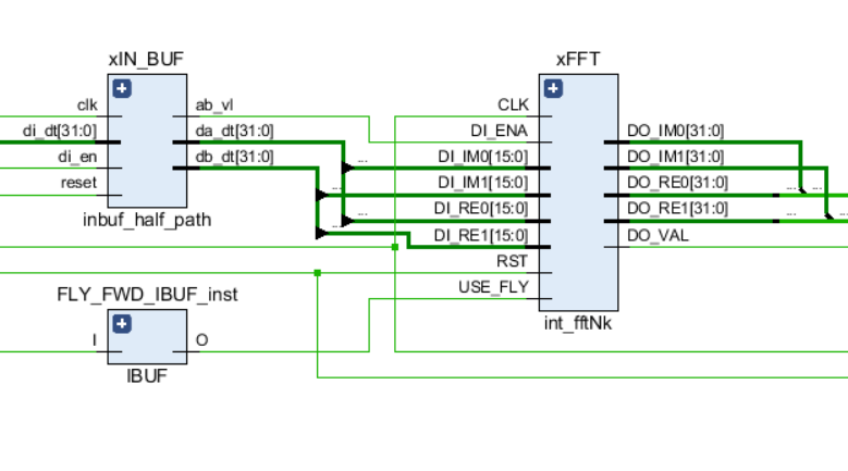
Like any other links in the circuit, the FFT has input control ports — a clock signal and a reset, as well as input and output data ports. In addition, the USE_FLY signal is used in the core, which allows you to dynamically turn off FFT butterflies for debugging processes or to view the original input stream.
The table below shows the amount of FPGA resources occupied depending on the NFFT FFT length for DATA_WIDTH = 16 and two digits TWDL_WIDTH = 16 and 24 bits.

The kernel with NFFT = 64K stably operates at a processing frequency FREQ = 375 MHz on a Kintex-7 (410T) chip.
A schematic graph of the FFT node is shown in the following figure:

For the convenience of understanding the features of certain components, here is a list of project files and a brief description in a hierarchical order:
* - for DSP48E1: 25 bits, for DSP48E2 - 27 bits.
** - from a certain stage of the FFT, you can use a fixed amount of block memory to store the turning coefficients, and calculate the intermediate coefficients using DSP48 nodes using the Taylor formula to the first derivative. Due to the fact that the memory resource is more important for the FFT, we can safely sacrifice the computing blocks for the sake of memory.
*** - input buffer and delay lines - make a significant contribution to the amount of FPGA memory resources
"Butterfly"
Anyone who has encountered the Fourier transform algorithm at least once knows that the basis of this algorithm is an elementary operation - the “butterfly”. It converts the input stream by multiplying the input data by the twiddle factor. For FFT, there are two classic conversion schemes - frequency decimation (DIF, decimation-in-frequency) and time decimation (DIT, decimation-in-time). The DIT algorithm is characterized by splitting the input sequence into two half-length sequences, and for the DIF algorithm - into two sequences of even and odd samples with a duration of NFFT. In addition, these algorithms are different mathematical operations for the operation "butterfly".
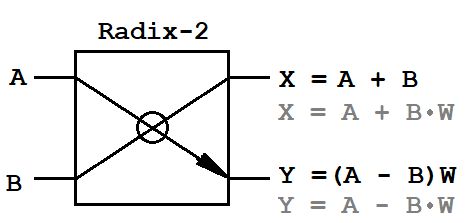
A, B - input pairs of complex samples,
X, Y - output pairs of complex samples,
W - complex turning factors.
Since the input data are complex values, the butterfly requires one complex multiplier (4 multiplication operations and 2 addition operations) and two complex adders (4 addition operations). This is the whole mathematical basis that must be implemented on the FPGA.
It should be noted that all mathematical operations on FPGA are often performed in additional code (2's complement). The FPGA multiplier can be implemented in two ways - on logic, using triggers and LUT tables, or on special DSP48 calculation blocks, which have long been firmly incorporated into all modern FPGAs. On logical blocks, multiplication is implemented using the Bout algorithm or its modifications; it occupies a decent amount of logical resources and does not always satisfy the time constraints at high frequencies of data processing. In this regard, multipliers on the FPGA in modern projects are almost always designed on the basis of DSP48 nodes and only occasionally on logic. The DSP48 node is a complex, complete cell that implements mathematical and logical functions. Basic operations: multiplication, addition, subtraction, accumulation, counter, logical operations (XOR, NAND, AND, OR, NOR), squaring, comparison of numbers, shift, etc. The following figure shows the DSP48E2 cell for the Xilinx Ultrascale + FPGA family.

By uncomplicated configuration of input ports, computing operations at the nodes and setting delays inside the node, you can make a high-speed mathematical data thresher.
Note that all top FPGA vendors in the design environment have standard and free IP cores for calculating mathematical functions based on the DSP48 node. They allow you to calculate primitive mathematical functions and expose various delays at the input and output of the node. In Xilinx, this is the IP-Core multiplier (ver. 12.0, 2018), which allows you to configure the multiplier to any input data width from 2 to 64 bits. In addition, you can specify the way to implement a multiplier - on logical resources or embedded DSP48 primitives.
Estimate how much logic the multiplier eats with the input data width on ports A and B = 64 bits. If you use the DSP48 nodes, then they will need only 16.

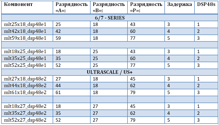
The main limitation imposed on the DSP48 cells is the input data width. In the DSP48E1 node, which is the base cell of the Xilinx 6 and 7 series FPGAs, the input ports for multiplication are: “A” - 25 bits, “B” - 18 - bits, Therefore, the result of the multiplication is a 43-bit number. For the Xilinx Ultrascale and Ultrascale + family, the node has undergone several changes, in particular, the capacity of the first port has grown by two bits: “A” - 27 bits, “B” - 18 - bits. In addition, the node itself is called DSP48E2.
In order not to be tied to a specific family and FPGA chip, to ensure “source code purity”, and to take into account all possible bit widths of input data, it was decided to design its own set of multipliers. This will allow for the most efficient implementation of complex multipliers for FFT “butterflies”, namely, multipliers and an adder-subtractor based on DSP48 blocks. The first input of the multiplier is the input data, the second input of the multiplier is the turning factors (the harmonic signal from the memory). A set of multipliers is implemented using the built-in UNISIM library, from which you need to connect the DSP48E1 and DSP48E2 primitives for further use in the project. A set of multipliers is presented in the table. It should be noted that:
A further increase in bit depth is not of interest within the framework of the task, for the reasons described below:
It is known that the greater the bit depth of the harmonic signal - the more accurately the number appears (the more signs in the fractional part). But the port size is B <25 bits due to the fact that for turning factors in the FFT nodes of this capacity is enough to ensure high-quality multiplication of the input stream with harmonic signal elements in the “butterflies” (for any real attainable FFT lengths on modern FPGAs). The typical value of the bitness of the turning coefficients in the tasks I implement is equal to 16 bits, 24 less often, 32 never.
The data width of the typical reception and registration nodes (ADC, DAC) is not great - from 8 to 16 bits, and rarely - 24 or 32 bits. Moreover, in the latter case, it is more efficient to use the floating-point data format according to the IEEE-754 standard. On the other hand, each “butterfly” stage in the FFT adds one bit of data to the output samples due to the execution of mathematical operations. For example, for a length of NFFT = 1024, log2 (NFFT) = 10 butterflies are used.
Consequently, the output bit depth will be ten bits greater than the input, WOUT = WIN + 10. In general, the formula looks like this:
WOUT = WIN + log2 (NFFT);
Example:
The width of the input stream WIN = 32 bits
The width of the turning factors TWD = 27,
The port “A” width from the list of implemented multipliers in this article does not exceed 52 bits. This means that the maximum number of FFT butterflies = 52-32 = 20. That is, it is possible to implement an FFT of up to 2 ^ 20 = 1M samples. (However, in practice, direct means is impossible due to the limited resources of even the most powerful FPGA crystals, but this relates to another topic and will not be considered in the article).
As you can see, this is one of the main reasons why I did not implement multipliers with a higher input port capacity. The used multipliers cover the full range of required values of the input data width and the turning factors for the task of calculating the integer FFT. In all other cases, you can use the floating-point FFT calculation!
Based on a simple example of multiplying two numbers that do not fit into the width of a standard DSP48 node, I will show how you can implement a wide data multiplier. The following figure shows its block diagram. The multiplier implements the multiplication of two signed numbers in the additional code, the width of the first operand X is 42 bits, the second Y is 18 bits. It contains two DSP48E2 nodes. To align the delays in the top node, two registers are used. This is done for the reason that in the upper adder you need to correctly add the numbers from the upper and lower nodes of the DSP48. Lower adder is not actually used. At the output of the lower node, there is an additional delay in the product to align the output number with time. The total delay is 4 cycles.

The product consists of two components:
Similar to a multiplier, an adder can be built on logical resources using a carry chain, or on DSP48 blocks. To achieve maximum throughput, the second method is preferred. One DSP48 primitive allows the addition operation to 48 bits, two nodes up to 96 bits. For the realizable task such digit capacity is quite enough. In addition, the DSP48 primitive has a special mode “SIMD MODE”, which parallelizes the built-in 48-bit ALU for several operations with different data of small bitness. That is, in the ONE mode, a full bit grid of 48 bits and two operands is used, and in the TWO mode, the bit grid is divided into several parallel streams of 24 bits each (4 operands). This mode, using only one adder, helps to reduce the amount of FPGA crystal resources occupied at small digits of the input samples (in the first stages of the calculation).
The operation of multiplying two numbers with digit capacity N and M in the binary additional code leads to an increase in the output digit capacity to P = N + M.
Example: for multiplying three-bit numbers, N = M = 3, the maximum positive number is +3 = (011) 2 , and the most negative number is 4 = (100) 2 . The high bit is responsible for the sign of the number. Therefore, the maximum possible number when multiplying is +16 = (010000) 2 , which is formed as a result of multiplying the two most negative numbers -4. The bit width of the output data is equal to the sum of the input bits P = N + M = 6 bits.
The operation of adding two numbers with digit capacity N and M in the binary additional code leads to an increase in the output digit capacity by one bit.
Example: we add two positive numbers, N = M = 3, the maximum positive number is 3 = (011) 2 , and the maximum negative number is 4 = (100) 2 . The high bit is responsible for the sign of the number. Therefore, the maximum positive number is 6 = (0110) 2 , and the maximum negative number is -8 = (1000) 2 . The bit width of the output is increased by one bit.
Truncation truncation from the top:
To minimize FPGA resources in the FFT algorithm, it was decided to never use the maximum possible negative number for the turning factors when multiplying the data in the butterfly. This amendment does not contribute to the outcome. For example, when using the 16-bit representation of the turning factors, the minimum number is -32768 = 0x8000, and the following number is -32767 = 0x8001. The error in replacing the most negative number with the nearest neighboring value will be ~ 0.003% and is fully acceptable for the implementation of the task.
By removing the minimum number in the product of two numbers, at each iteration it is possible to reduce one unused leading digit. Example: data - 4 = (100) 2 , coefficient +3 = (011) 2 . The result of the multiplication = -12 = (110100) 2 . The fifth bit can be discarded, because it duplicates the neighboring, fourth, sign bit.
Truncation bottom:
Obviously, multiplying the input signal for a harmonic effect in a “butterfly” does not require pulling the output bit into the next butterflies, but rounding or truncation is required. The rotating multipliers are presented in a convenient M-bit format, but in reality this is the usual sine and cosine normalized to one. That is, the number 0x8000 = -1, and the number 0x7FFF = +1. Therefore, the result of the multiplication is necessarily truncated to the original data width (that is, the M bits from the turning factors are truncated below). In all implementations of FFT, as I have seen, the turning factors are normalized to 1 in one way or another. Therefore, from the result of the multiplication it is necessary to take the bits in the following grid [N + M-1-1: M-1]. The most significant bit is not used (we subtract an additional 1), the least significant ones are truncated.
Adding / subtracting data in butterfly operations is in no way minimized, and only this operation contributes to the increase in the output data by one bit at each stage of the calculation .
Note that at the first stage of the FFT DIT algorithm or at the last stage of the FFT DIF algorithm, the data must be multiplied by the turning factor with the zero index W0 = {Re, Im} = {1, 0}. Due to the fact that multiplication by one and zero is a primitive operation, they can not be executed. In this case, the operation of complex multiplication is not required at all: the real and imaginary components undergo a "turn" without any changes. In the second stage, two coefficients are used: W0 = {Re, Im} = {1, 0} and W1 = {Re, Im} = {0, -1}. Similarly, operations can be reduced to elementary transformations and a multiplexer can be used to select the output sample. This allows you to significantly save DSP48 blocks on the first two butterflies.
The complex multiplier is constructed in the same way - on the basis of multipliers and adder-subtractor, however, for some variants of the input data width, additional resources will not be needed, which will be discussed below.
The input buffer and delay lines and cross-switches are similar to those described in the previous article. The rolling multipliers became integer with configurable bit depth. For the rest, there is no global change in the design of the FFT core.
The source code for the FFT INTFFTK kernel on VHDL (including basic operations and a set of multipliers) and Matlab / Octave m-scripts are available in my github profile .
In the course of development, a new core FFT was designed, which provides greater performance compared to analogues. A bundle of FFT and OBPF cores does not require conversion to the natural order, and the maximum conversion length is limited only by the FPGA resources. Double parallelism allows processing of doubled frequency input streams, which IP-CORE Xilinx cannot do. The resolution at the output of the integer FFT increases linearly depending on the number of conversion stages.
In the last article I wrote about future plans: Radix-4 FFT cores, Radix-8, Ultra-Long FFT for many millions of points, FFT-FP32 (in IEEE-754 format). In short, they are practically all allowed, but for one reason or another, at the moment they cannot be made public. An exception is the FFT Radix-8 algorithm, which I didn’t even add to (difficult and lazy).
Once again, I thank dsmv2014 , who always welcomed my adventurous ideas. Thanks for attention!
Added the SCALED FFT / IFFT option to the source codes. On each butterfly truncate LSB is truncated. Output data width = input bit.
In addition, I will give two graphs of the passage of a real signal through the FPGA to show the integral property of the transformation, that is: how truncation affects the result of the accumulation of error at the FFT output. It is known from theory that as a result of the Fourier transform, the signal-to-noise ratio deteriorates when the input signal is truncated relative to the non-truncated version.
Example: The input amplitude swing is 6 bits. The signal is a sinusoid at 128 PF count. NFFT = 1024 samples, DATA_WIDTH = 16, TWDL_WIDTH = 16.
As you can see, the SCALED variant “did not pull out” the sinusoid from the noise, while the UNSCALED variant showed a good result.
Once customers asked me if I had any integer FFT in my projects, to which I always replied that it was already done by others in the form of ready-made, albeit crooked, but free IP cores (Altera / Xilinx) - take and use. However, these kernels are not optimal , possess a set of "features" and require further refinement. In this connection, having gone to the next planned vacation, which I did not want to spend foolishly, I started to implement a configurable kernel of the integer FFT.
KDPV (process of debugging data overflow errors)
')
In the article I want to tell you what ways and means implemented mathematical operations when calculating the fast Fourier transform in the integer format on modern FPGA crystals. The basis of any FFT is the node, which is called "butterfly". In a butterfly, mathematical actions are realized - addition, multiplication and subtraction. It is about the implementation of the "butterfly" and its completed nodes that the story will go first. Based on the current FPGA family of Xilinx firms - these are the Ultrascale and Ultrascale + series, as well as the older 6- (Virtex) and 7- (Artix, Kintex, Virtex) series are affected. Older series in modern projects are not of interest in 2018. The purpose of the article is to reveal the implementation features of custom cores of digital signal processing using the example of an FFT.
Introduction
It's no secret that the FFT algorithms have become firmly established in the life of digital signal processing engineers, and therefore, this tool is needed all the time. Leading FPGA manufacturers, such as Altera / Xilinx, already have flexible, configurable FFT / IFFT cores, but they have a number of limitations and features, and therefore I have often had to use my own experiences. So this time I had to implement the FFT in the integer format according to the Radix-2 scheme on the FPGA. In my last article, I already did a floating-point FFT , and from there you know that the algorithm with double parallelism is used to implement the FFT, that is, the core can process two complex samples at the same frequency . This is a key feature of the FFT, which is not found in the ready-made Xilinx FFT cores.
Example: it is required to develop an FFT node that performs continuous operation of the input stream of complex numbers at a frequency of 800 MHz. The core from Xilinx does not pull this (actually achievable processing clock frequencies in modern FPGAs are about 300-400 MHz), or it will require to somehow decimate the input stream. The custom kernel allows, without prior intervention, clocking two input samples at 400 MHz instead of one reference at 800 MHz. Another minus of the Xilinx FFT core is related to the inability to receive the input stream in a bit-reverse order . In this connection, an enormous resource of memory of the FPGA crystal is spent for rearranging data into a normal order. For the tasks of fast convolution of signals, when two FFT nodes are located one after another, this can be a critical moment, that is, the task simply does not fall into the selected FPGA chip. Custom FFT core allows you to receive data in the normal order, and output - in a bit-reverse, and the inverse FFT core - on the contrary, receives data in a bit-reverse order, and gives in the normal. Two buffers are saved at once for data permutation !!!
Since most of the material of this article could intersect with the previous one , I decided to focus on uncovering the topic of mathematical operations in an integer format on FPGA for the implementation of FFT.
FFT core parameters
- NFFT - the number of butterflies (length of the FFT),
- DATA_WIDTH - input data width (4-32),
- TWDL_WIDTH - the width of the turning factors (8-27).
- SERIES - sets the FPGA family on which the FFT is implemented (“NEW” - Ultrascale, “OLD” - 6/7 Xilinx FPGA series).
Like any other links in the circuit, the FFT has input control ports — a clock signal and a reset, as well as input and output data ports. In addition, the USE_FLY signal is used in the core, which allows you to dynamically turn off FFT butterflies for debugging processes or to view the original input stream.
The table below shows the amount of FPGA resources occupied depending on the NFFT FFT length for DATA_WIDTH = 16 and two digits TWDL_WIDTH = 16 and 24 bits.
The kernel with NFFT = 64K stably operates at a processing frequency FREQ = 375 MHz on a Kintex-7 (410T) chip.
Project structure
A schematic graph of the FFT node is shown in the following figure:
For the convenience of understanding the features of certain components, here is a list of project files and a brief description in a hierarchical order:
- FFT cores:
- int_fftNk - FFT node, Radix-2 circuit, frequency decimation (DIF), input stream - normal, output - bit-reverse.
- int_ifftNk - OBPF node, Radix-2 scheme, time decimation (DIT), input stream - bit-reverse, output - normal.
- Butterflies:
- int_dif2_fly - Radix-2 butterfly, frequency decimation,
- int_dit2_fly - Radix-2 butterfly, time decimation,
- Complex multipliers:
- int_cmult_dsp48 - common configurable multiplier, includes:
- int_cmult18x25_dsp48 - a multiplier for small data digits and turning factors,
- int_cmult_dbl18_dsp48 - doubled multiplier, the width of the turning factors to 18 bits,
- int_cmult_dbl35_dsp48 - doubled multiplier, the width of the turning factors to 25 * bit,
- int_cmult_trpl18_dsp48 - the triple multiplier, the width of the turning factors to 18 bits,
- int_cmult_trpl52_dsp48 - the triple multiplier, the width of the turning factors is up to 25 * bits,
- Multipliers:
- mlt42x18_dsp48e1 - a multiplier with operand widths up to 42 and 18 bits based on DSP48E1,
- mlt59x18_dsp48e1 - a multiplier with operand sizes up to 59 and 18 bits based on DSP48E1,
- mlt35x25_dsp48e1 - a multiplier with operand sizes up to 35 and 25 bits based on DSP48E1,
- mlt52x25_dsp48e1 - a multiplier with the resolution of the operands of up to 52 and 25 bits based on DSP48E1,
- mlt44x18_dsp48e2 - a multiplier with operands of up to 44 and 18 bits based on DSP48E2,
- mlt61x18_dsp48e2 - a multiplier with operand widths up to 61 and 18 bits based on DSP48E2,
- mlt35x27_dsp48e2 - a multiplier with operand sizes up to 35 and 27 bits based on DSP48E2,
- mlt52x27_dsp48e2 is a multiplier with operand widths up to 52 and 27 bits based on DSP48E2.
- Adder:
- int_addsub_dsp48 - universal adder, operand width up to 96 bits.
- Delay lines:
- int_delay_line - baseline delay line, provides data swapping between butterflies,
- int_align_fft - alignment of input data and turning factors at the input of the FFT butterfly,
- int_align_fft - alignment of the input data and the turning factors at the input of the IFFT butterfly,
- Turning factors:
- rom_twiddle_int is a generator of turning factors, with a certain length, the FFT counts the coefficients on the basis of DSP FPGA cells,
- row_twiddle_tay - the turning factors generator using the Taylor series (NFFT> 2K) **.
- Data buffer:
- inbuf_half_path is the input buffer, receives the stream in the normal mode and outputs two sequences of samples shifted by half the FFT length ***,
- outbuf_half_path - output buffer, collects two sequences and outputs one continuous equal to the length of the FFT,
- iobuf_flow_int2 - the buffer operates in two modes: it receives the stream in the Interleave-2 mode and provides two sequences shifted by half the length of the FFT. Or vice versa, depending on the “BITREV” option.
- int_bitrev_ord is a simple data converter from natural order to bit-reverse.
* - for DSP48E1: 25 bits, for DSP48E2 - 27 bits.
** - from a certain stage of the FFT, you can use a fixed amount of block memory to store the turning coefficients, and calculate the intermediate coefficients using DSP48 nodes using the Taylor formula to the first derivative. Due to the fact that the memory resource is more important for the FFT, we can safely sacrifice the computing blocks for the sake of memory.
*** - input buffer and delay lines - make a significant contribution to the amount of FPGA memory resources
"Butterfly"
Anyone who has encountered the Fourier transform algorithm at least once knows that the basis of this algorithm is an elementary operation - the “butterfly”. It converts the input stream by multiplying the input data by the twiddle factor. For FFT, there are two classic conversion schemes - frequency decimation (DIF, decimation-in-frequency) and time decimation (DIT, decimation-in-time). The DIT algorithm is characterized by splitting the input sequence into two half-length sequences, and for the DIF algorithm - into two sequences of even and odd samples with a duration of NFFT. In addition, these algorithms are different mathematical operations for the operation "butterfly".
A, B - input pairs of complex samples,
X, Y - output pairs of complex samples,
W - complex turning factors.
Since the input data are complex values, the butterfly requires one complex multiplier (4 multiplication operations and 2 addition operations) and two complex adders (4 addition operations). This is the whole mathematical basis that must be implemented on the FPGA.
Multiplier
It should be noted that all mathematical operations on FPGA are often performed in additional code (2's complement). The FPGA multiplier can be implemented in two ways - on logic, using triggers and LUT tables, or on special DSP48 calculation blocks, which have long been firmly incorporated into all modern FPGAs. On logical blocks, multiplication is implemented using the Bout algorithm or its modifications; it occupies a decent amount of logical resources and does not always satisfy the time constraints at high frequencies of data processing. In this regard, multipliers on the FPGA in modern projects are almost always designed on the basis of DSP48 nodes and only occasionally on logic. The DSP48 node is a complex, complete cell that implements mathematical and logical functions. Basic operations: multiplication, addition, subtraction, accumulation, counter, logical operations (XOR, NAND, AND, OR, NOR), squaring, comparison of numbers, shift, etc. The following figure shows the DSP48E2 cell for the Xilinx Ultrascale + FPGA family.
By uncomplicated configuration of input ports, computing operations at the nodes and setting delays inside the node, you can make a high-speed mathematical data thresher.
Note that all top FPGA vendors in the design environment have standard and free IP cores for calculating mathematical functions based on the DSP48 node. They allow you to calculate primitive mathematical functions and expose various delays at the input and output of the node. In Xilinx, this is the IP-Core multiplier (ver. 12.0, 2018), which allows you to configure the multiplier to any input data width from 2 to 64 bits. In addition, you can specify the way to implement a multiplier - on logical resources or embedded DSP48 primitives.
Estimate how much logic the multiplier eats with the input data width on ports A and B = 64 bits. If you use the DSP48 nodes, then they will need only 16.
The main limitation imposed on the DSP48 cells is the input data width. In the DSP48E1 node, which is the base cell of the Xilinx 6 and 7 series FPGAs, the input ports for multiplication are: “A” - 25 bits, “B” - 18 - bits, Therefore, the result of the multiplication is a 43-bit number. For the Xilinx Ultrascale and Ultrascale + family, the node has undergone several changes, in particular, the capacity of the first port has grown by two bits: “A” - 27 bits, “B” - 18 - bits. In addition, the node itself is called DSP48E2.
In order not to be tied to a specific family and FPGA chip, to ensure “source code purity”, and to take into account all possible bit widths of input data, it was decided to design its own set of multipliers. This will allow for the most efficient implementation of complex multipliers for FFT “butterflies”, namely, multipliers and an adder-subtractor based on DSP48 blocks. The first input of the multiplier is the input data, the second input of the multiplier is the turning factors (the harmonic signal from the memory). A set of multipliers is implemented using the built-in UNISIM library, from which you need to connect the DSP48E1 and DSP48E2 primitives for further use in the project. A set of multipliers is presented in the table. It should be noted that:
- The operation of multiplying numbers leads to an increase in the digit of the product as the sum of the digits of the operands.
- Each of the multipliers 25x18 and 27x18 are duplicated, in fact - this is one component for different families.
- The greater the stage of parallelism of the operation - the greater the delay in the calculation and the greater the amount of resources occupied.
- With a smaller bit width at the input “B”, it is possible to realize multipliers with a higher bit width at another input.
- The main limitation in increasing the bit depth is the “B” port (the real port of the DSP48 primitive) and the internal shift register to 17-bit.
A further increase in bit depth is not of interest within the framework of the task, for the reasons described below:
The width of the turning factors
It is known that the greater the bit depth of the harmonic signal - the more accurately the number appears (the more signs in the fractional part). But the port size is B <25 bits due to the fact that for turning factors in the FFT nodes of this capacity is enough to ensure high-quality multiplication of the input stream with harmonic signal elements in the “butterflies” (for any real attainable FFT lengths on modern FPGAs). The typical value of the bitness of the turning coefficients in the tasks I implement is equal to 16 bits, 24 less often, 32 never.
The width of the input samples
The data width of the typical reception and registration nodes (ADC, DAC) is not great - from 8 to 16 bits, and rarely - 24 or 32 bits. Moreover, in the latter case, it is more efficient to use the floating-point data format according to the IEEE-754 standard. On the other hand, each “butterfly” stage in the FFT adds one bit of data to the output samples due to the execution of mathematical operations. For example, for a length of NFFT = 1024, log2 (NFFT) = 10 butterflies are used.
Consequently, the output bit depth will be ten bits greater than the input, WOUT = WIN + 10. In general, the formula looks like this:
WOUT = WIN + log2 (NFFT);
Example:
The width of the input stream WIN = 32 bits
The width of the turning factors TWD = 27,
The port “A” width from the list of implemented multipliers in this article does not exceed 52 bits. This means that the maximum number of FFT butterflies = 52-32 = 20. That is, it is possible to implement an FFT of up to 2 ^ 20 = 1M samples. (However, in practice, direct means is impossible due to the limited resources of even the most powerful FPGA crystals, but this relates to another topic and will not be considered in the article).
As you can see, this is one of the main reasons why I did not implement multipliers with a higher input port capacity. The used multipliers cover the full range of required values of the input data width and the turning factors for the task of calculating the integer FFT. In all other cases, you can use the floating-point FFT calculation!
The implementation of the "wide" multiplier
Based on a simple example of multiplying two numbers that do not fit into the width of a standard DSP48 node, I will show how you can implement a wide data multiplier. The following figure shows its block diagram. The multiplier implements the multiplication of two signed numbers in the additional code, the width of the first operand X is 42 bits, the second Y is 18 bits. It contains two DSP48E2 nodes. To align the delays in the top node, two registers are used. This is done for the reason that in the upper adder you need to correctly add the numbers from the upper and lower nodes of the DSP48. Lower adder is not actually used. At the output of the lower node, there is an additional delay in the product to align the output number with time. The total delay is 4 cycles.
The product consists of two components:
- The younger part: P1 = '0' & X [16: 0] * Y [17: 0];
- The major part: P2 = X [42:17] * Y [17: 0] + (P1 >> 17);
Adder
Similar to a multiplier, an adder can be built on logical resources using a carry chain, or on DSP48 blocks. To achieve maximum throughput, the second method is preferred. One DSP48 primitive allows the addition operation to 48 bits, two nodes up to 96 bits. For the realizable task such digit capacity is quite enough. In addition, the DSP48 primitive has a special mode “SIMD MODE”, which parallelizes the built-in 48-bit ALU for several operations with different data of small bitness. That is, in the ONE mode, a full bit grid of 48 bits and two operands is used, and in the TWO mode, the bit grid is divided into several parallel streams of 24 bits each (4 operands). This mode, using only one adder, helps to reduce the amount of FPGA crystal resources occupied at small digits of the input samples (in the first stages of the calculation).
The increase in data width
The operation of multiplying two numbers with digit capacity N and M in the binary additional code leads to an increase in the output digit capacity to P = N + M.
Example: for multiplying three-bit numbers, N = M = 3, the maximum positive number is +3 = (011) 2 , and the most negative number is 4 = (100) 2 . The high bit is responsible for the sign of the number. Therefore, the maximum possible number when multiplying is +16 = (010000) 2 , which is formed as a result of multiplying the two most negative numbers -4. The bit width of the output data is equal to the sum of the input bits P = N + M = 6 bits.
The operation of adding two numbers with digit capacity N and M in the binary additional code leads to an increase in the output digit capacity by one bit.
Example: we add two positive numbers, N = M = 3, the maximum positive number is 3 = (011) 2 , and the maximum negative number is 4 = (100) 2 . The high bit is responsible for the sign of the number. Therefore, the maximum positive number is 6 = (0110) 2 , and the maximum negative number is -8 = (1000) 2 . The bit width of the output is increased by one bit.
Algorithm Considerations
Truncation truncation from the top:
To minimize FPGA resources in the FFT algorithm, it was decided to never use the maximum possible negative number for the turning factors when multiplying the data in the butterfly. This amendment does not contribute to the outcome. For example, when using the 16-bit representation of the turning factors, the minimum number is -32768 = 0x8000, and the following number is -32767 = 0x8001. The error in replacing the most negative number with the nearest neighboring value will be ~ 0.003% and is fully acceptable for the implementation of the task.
By removing the minimum number in the product of two numbers, at each iteration it is possible to reduce one unused leading digit. Example: data - 4 = (100) 2 , coefficient +3 = (011) 2 . The result of the multiplication = -12 = (110100) 2 . The fifth bit can be discarded, because it duplicates the neighboring, fourth, sign bit.
Truncation bottom:
Obviously, multiplying the input signal for a harmonic effect in a “butterfly” does not require pulling the output bit into the next butterflies, but rounding or truncation is required. The rotating multipliers are presented in a convenient M-bit format, but in reality this is the usual sine and cosine normalized to one. That is, the number 0x8000 = -1, and the number 0x7FFF = +1. Therefore, the result of the multiplication is necessarily truncated to the original data width (that is, the M bits from the turning factors are truncated below). In all implementations of FFT, as I have seen, the turning factors are normalized to 1 in one way or another. Therefore, from the result of the multiplication it is necessary to take the bits in the following grid [N + M-1-1: M-1]. The most significant bit is not used (we subtract an additional 1), the least significant ones are truncated.
Adding / subtracting data in butterfly operations is in no way minimized, and only this operation contributes to the increase in the output data by one bit at each stage of the calculation .
Note that at the first stage of the FFT DIT algorithm or at the last stage of the FFT DIF algorithm, the data must be multiplied by the turning factor with the zero index W0 = {Re, Im} = {1, 0}. Due to the fact that multiplication by one and zero is a primitive operation, they can not be executed. In this case, the operation of complex multiplication is not required at all: the real and imaginary components undergo a "turn" without any changes. In the second stage, two coefficients are used: W0 = {Re, Im} = {1, 0} and W1 = {Re, Im} = {0, -1}. Similarly, operations can be reduced to elementary transformations and a multiplexer can be used to select the output sample. This allows you to significantly save DSP48 blocks on the first two butterflies.
The complex multiplier is constructed in the same way - on the basis of multipliers and adder-subtractor, however, for some variants of the input data width, additional resources will not be needed, which will be discussed below.
The input buffer and delay lines and cross-switches are similar to those described in the previous article. The rolling multipliers became integer with configurable bit depth. For the rest, there is no global change in the design of the FFT core.
Features of the FFT core INT_FFTK
- Fully pipelined data processing circuit.
- NFFT transform length = 8-512K points.
- Flexible adjustment of NFFT conversion length.
- Integer format of input data, bit width is configured.
- Integer format of the turning factors, the digit capacity is configured.
- Compact storage of turning factors through expansion in a Taylor series to the first derivative.
- The growth of digit capacity at each stage of computation and at the output of the core!
- Storage of a quarter of a period of coefficients to save crystal resources.
- FFT: input data - in the direct order, at the output in binary inverse.
- OBPF: input data in binary-inverse order, output - in the forward.
- Conveyor processing scheme with double parallelism. Radix-2.
- The minimum non-breaking data burst is NFFT samples *.
- High computation speed and small amount of resources.
- Realization on the last FPGA crystals (Virtex-6, 7-Series, Ultrascale).
- Kernel frequency ~ 375MHz at Kintex-7
- Description Language - VHDL.
- No need for a bitreverse transform operation for a bunch of FFT + OBPF.
- Open Source project without the inclusion of third-party IP-Cores.
Source
The source code for the FFT INTFFTK kernel on VHDL (including basic operations and a set of multipliers) and Matlab / Octave m-scripts are available in my github profile .
Conclusion
In the course of development, a new core FFT was designed, which provides greater performance compared to analogues. A bundle of FFT and OBPF cores does not require conversion to the natural order, and the maximum conversion length is limited only by the FPGA resources. Double parallelism allows processing of doubled frequency input streams, which IP-CORE Xilinx cannot do. The resolution at the output of the integer FFT increases linearly depending on the number of conversion stages.
In the last article I wrote about future plans: Radix-4 FFT cores, Radix-8, Ultra-Long FFT for many millions of points, FFT-FP32 (in IEEE-754 format). In short, they are practically all allowed, but for one reason or another, at the moment they cannot be made public. An exception is the FFT Radix-8 algorithm, which I didn’t even add to (difficult and lazy).
Once again, I thank dsmv2014 , who always welcomed my adventurous ideas. Thanks for attention!
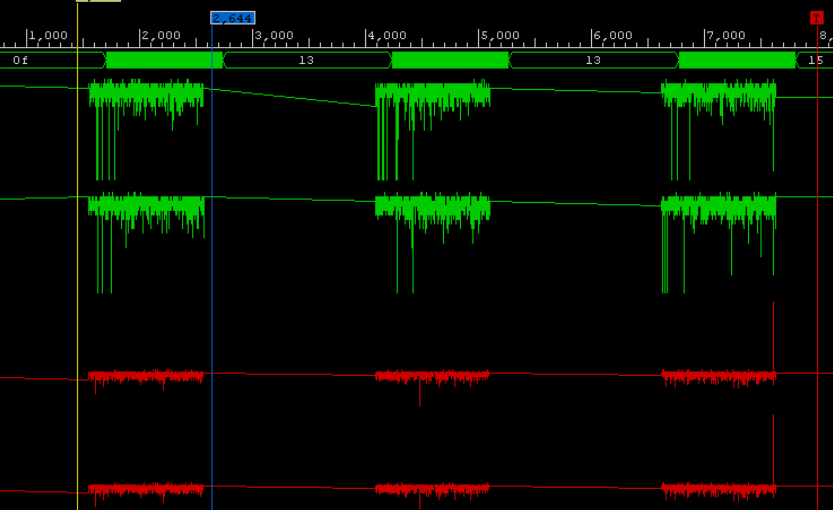
UPDATE 2018/08/22
Added the SCALED FFT / IFFT option to the source codes. On each butterfly truncate LSB is truncated. Output data width = input bit.
In addition, I will give two graphs of the passage of a real signal through the FPGA to show the integral property of the transformation, that is: how truncation affects the result of the accumulation of error at the FFT output. It is known from theory that as a result of the Fourier transform, the signal-to-noise ratio deteriorates when the input signal is truncated relative to the non-truncated version.
Example: The input amplitude swing is 6 bits. The signal is a sinusoid at 128 PF count. NFFT = 1024 samples, DATA_WIDTH = 16, TWDL_WIDTH = 16.
Two graphs of the signal passing through the FFT
Fig. 1 The signal-to-noise ratio is weak:

Fig. 2 Signal-to-noise ratio strong:

Fig. 2 Signal-to-noise ratio strong:
- Pink - UNSCALED FFT,
- Blue - SCALED FFT.
As you can see, the SCALED variant “did not pull out” the sinusoid from the noise, while the UNSCALED variant showed a good result.
Source: https://habr.com/ru/post/420517/
All Articles