Photon Artificial Neural Network
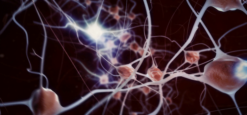
In one of the previous articles, we already got acquainted with one of the studies in the field of neuromorphic systems. Today we will again touch on this topic, but it will not be about creating an artificial nerve cell, but about how to combine these cells into one working network. After all, the human brain is like the most complex cobweb in the world, consisting of billions of intersections and connections of neurons. The researchers suggested that using light instead of electricity would greatly simplify the process of creating an artificial neural network comparable in complexity to the human brain. In addition to loud words, complex calculations and far from one experience, the scientists provided a working demo version of their device. How does it work, what are its features and what does it carry for the future of neuromorphic technologies? Answers to all questions are hidden in the report of researchers. It remains to find them. Go.
Scientists from NIST (National Institute of Standards and Technology / National Institute of Standards and Technology) have created a chip capable of using light signals, since it has two “layers” of photonic waveguides. The latter convert light streams into narrow bands for transmitting optical signals. According to scientists, this development will allow for the implementation of complex signal routing systems, which can be expanded even by adding additional chips.
Device structure
')
It is worth noting that the photon collector, experimentally described in the study, works regardless of the wavelength or time multiplexing * .
Temporary multiplexing * - transmission of several signals simultaneously over the same channel.

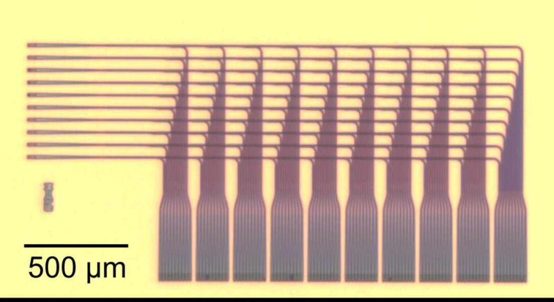
Image number 1
The basis of the collector structure is 2 vertical integrated planes of waveguides. The lower plane (P 1 ) faces east, while the second (P 2 ) faces south, which avoids intersections.
The light from P 1 , collected from each input node, is directed towards P 2 when it begins to move in the direction of the east. This routing reduces the number of waveguides involved, since each incoming signal is routed using a star connector * .
The star connector * is a device that receives an incoming signal and distributes it to several outgoing signals.The collector is implemented from two layers of a neural network with feedback interconnected:
- 10 ascending neurons;
- 10 descending neurons with 100 synapses.
The image 1c shows a diagram of a separate part of the system, describing the structure of the reservoir layers.
Remark: the report uses abbreviations associated with images 1b and 1c , namely T x (transmitters of the first layer of neurons) and S x, y (synapses / receivers of neurons of the second layer). Thus, for example, S 8.3 is the synapse of the third receiver, which receives the signal from the eighth transmitter (T 8 ).
This network structure allows each input node to form a group of 10 outgoing flows, which together represent the entire input array. Each group acts like synapses (receivers) for a particular descending neuron. This structural feature is demonstrated in image 1b .
The purpose of the collector is to direct each input to one synapse of each output, following the specified power distribution pattern.
Researchers have created two versions of the system:
- uniform - each outgoing synapse is provided with the same power;
- Gaussian - the synapse from the middle neurons of the ascending layer receives most of the power, and the synapses on the periphery of the neurons - much less.
For automatic generation of templates for both variants, a script was written, the variables of which were responsible for the number of neurons and the intensity distribution profiles.
The most important element of the system is the so-called tap and transfer device shown in image 1e . This device consists of a beam catcher and an interplane coupler (hereinafter referred to as IPC ), located as close as possible to each other. The task of the device is to divert a certain part of the bus power to a perpendicular waveguide on the upper plane.
Waveguides P 1 and P 2 adiabatically taper and expand to a distance of 1.5 μm (the combination of the red and blue lines in image 1e ) in order to minimize the scattering loss along its entire length.
To clarify, the waveguide P 1 tapers to a width of 400 nm at a distance of 12 μm, and then returns to its original width after 18 μm. Further, P 1 tapers to its minimum width of 200 nm over 12 μm. P 2 , in turn, repeats this pattern only in reverse order. As a result, the total length of the IPC is 42 microns.
When the network has such dimensions, it is extremely important to provide it with an impressive dynamic range of power ratios, which will allow achieving uniform or Gaussian distribution.
To meet this requirement, the collector uses three connecting gaps and a variable connection length, which makes it possible to successfully expand the power distribution range of the network.
The connecting gap is selected by the script from the lookup table, where the data of the previous calculations of the withdrawal coefficients are collected.
The values of the three gaps are as follows: 300 nm, 400 nm and 500 nm. And the length of the connection varies from 2.7 microns to 19 microns.
Manufacturing collector
The photon collector was manufactured within the walls of the Boulder Microfabrication Facility of the National Institute of Standards and Technology.
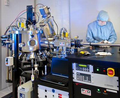
Inside the laboratory: the curator of the “clean room”, John Nibarger, examines a holder for a plate intended for a deposition instrument of sprayed materials for spraying precious metals.
The diameter of the silicon wafer was 77 mm.
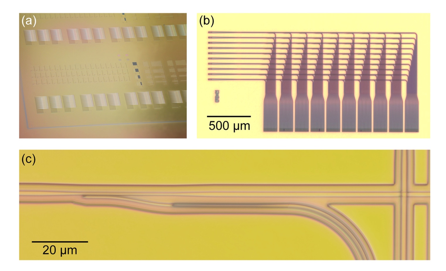
Image number 2: optical images made samples
The plane of the two waveguides in the samples consists of a SiN film (silicon nitride), 400 nm thick with an interplanar spacing of 1.2 μm and a nominal width of 800 nm. The material for the SiN film was deposited at very low temperatures (24, 25 and 40 ° C) in order to minimize mechanical stress and the mismatch of thermal expansion.
The SiN film had a refractive index of 1.96, and the rate of wave propagation loss was ∼5 dB / cm at a wavelength λ = 1310 nm.
From all sides, the waveguides are lined with plasma deposited SiO 2 (silicon dioxide).
Uniformly distributed collector
As we have already understood, regardless of the incoming power, each connected output synapse should account for the same part of the power. For example, having directed the light to the input node Tx, we should see the following power distribution: S x, 1 = S x, 2 = S x, 3 · · = S x, 10 .
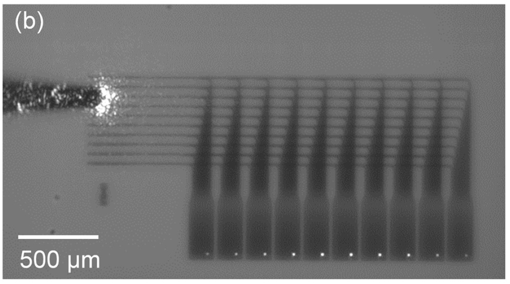
Image number 3b: infrared image of the collector, which shows how the light comes from the outgoing node
In order to satisfy this requirement, the distribution coefficient ranged from 0.1 to 0.5.
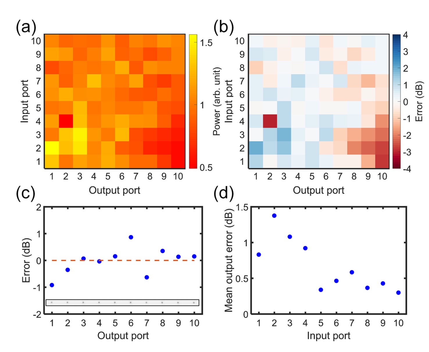
Image number 4
Image 4a shows the measured intensity indices, and on 4b all errors are recorded. And here we see that despite some errors, most of the synapses show good uniformity.
The sample shows the level of power uniformity of outgoing nodes for T 8 (input) ( 4c ).
Errors in turn are calculated as the deviation of each point from the mean. In image 4d, the mean value was measured from the absolute value of the errors in each row in image 4b . By combining all the data calculations, the researchers obtained an average error value of 0.7 dB.
Another important parameter to study was the spectral dependence of the collector with a uniform distribution. For this, a connection was established with only one input node T 8 , after which observations were made of changes in uniformity at the output with a wavelength scan.
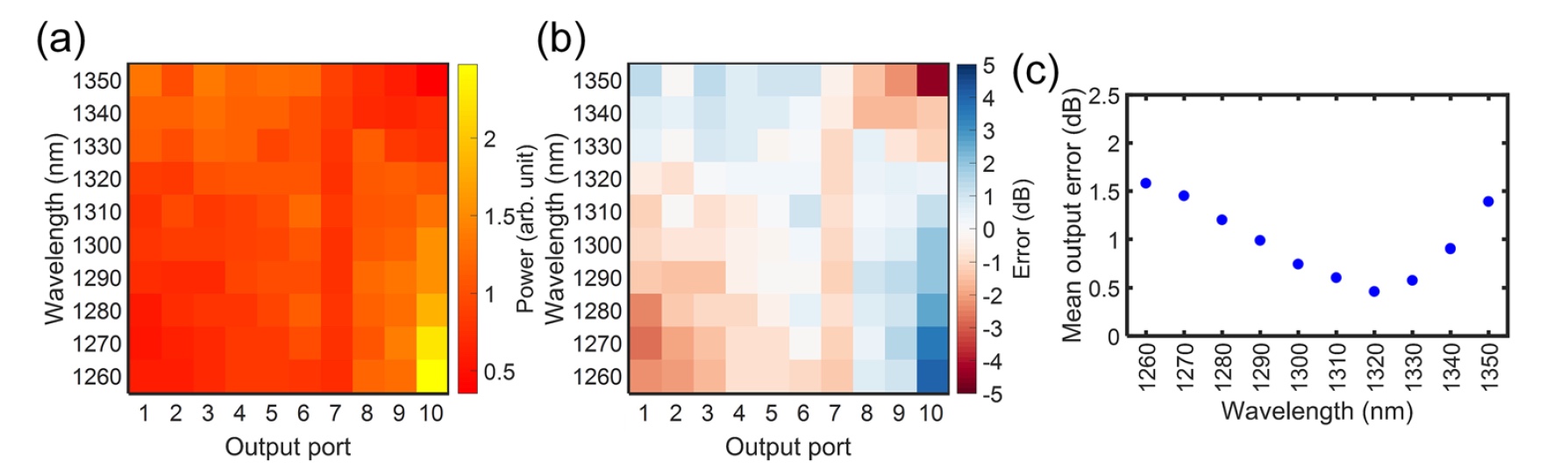
Image number 5
Image 5a shows the power versus wavelength. 5b displays all errors.
From graph 5c, it can be seen that the smallest average error value is 0.46 dB, observed at a wavelength of 1320 nm. This parameter does not rise above 1 dB even with a passband of 50 nm.
Gaussian collector
This collector is made in such a way that synapses receive power according to the principle of a Gaussian envelope.
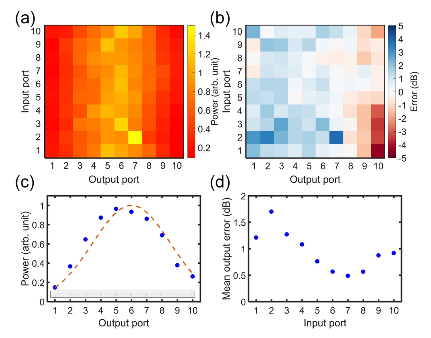
Image number 6
The overlay of the envelope on the experimentally determined synaptic power distribution for the input node T 8 showed excellent agreement ( 6c ).
Otherwise, the measurements were carried out according to the same scheme as with the previous collector.
Image 6a is a set of indicators of the dependence of power on the wavelength. 6b - errors.
Graph 6d is the average magnitude of the errors, calculated for all the rows in 6b . This figure was 0.9 dB.
Next was the measurement of spectral dependence. As with the previous collector, only the T 8 node participated in the measurements.
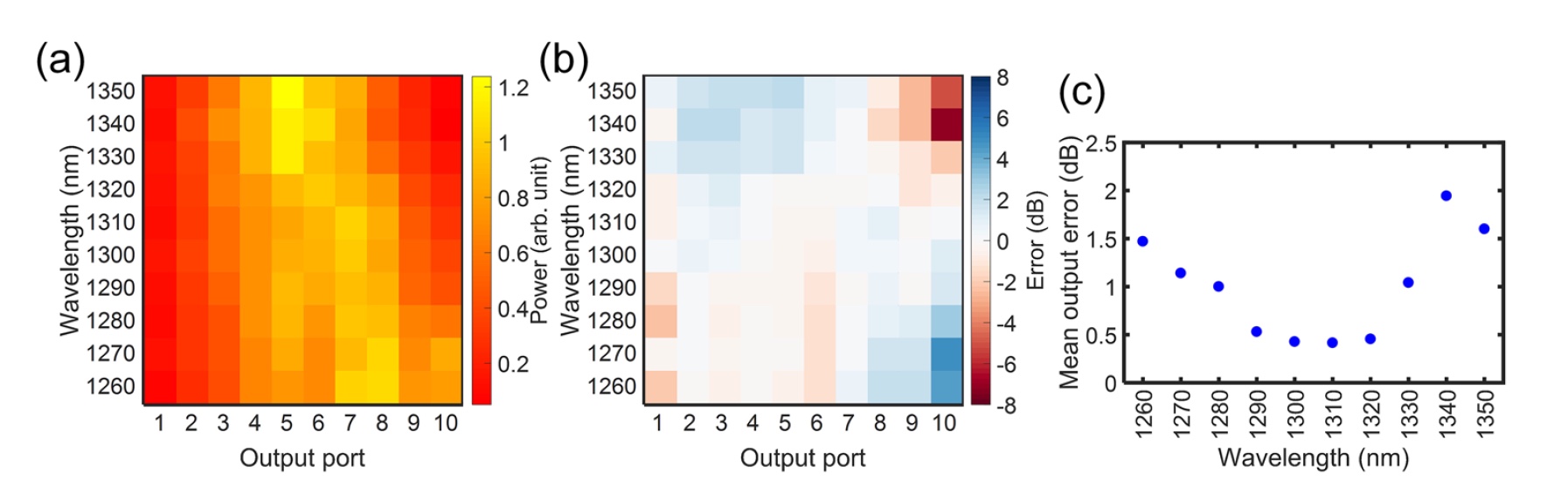
Image number 7
The dependence of power on the wavelength is shown in image 7a , and the error in 7b .
Also from image 7a , the movement of the barycenter * of the envelope towards the synapse with the smallest number is seen with increasing wavelength.
Barycenter * - arithmetic average position of all points of the figure.The smallest error value, 0.42 dB, was observed at a wavelength of 1310 nm, as shown in the 7c graph.
Taking into account the fact that both variants of the collector have the smallest error value observed at approximately the same wavelength, it can be argued that the retraction coefficient can be sufficiently calibrated at a wavelength of 1310-1320 nm.
Summarizing
Measurements of the number of errors and their average in both versions of the collectors made it clear that the output nodes with a large number have a lack of power, especially if they are connected to the nodes with a smaller number. Scientists have concluded that this is due to a large number of intersections of these waveguide routes, and this increases the loss compared to other routes. In addition, the distribution loss accumulates up to 1 dB for the longest routes, which affects the uniformity of the power distribution.
Another type of observed errors is dark and light synapses, which are clearly visible in the images above (for example, the synapse S 2.7 in image 6b ). Such a defect is most likely associated with mechanical damage during planarization (removal of irregularities from the surface of the plate).
It is worth noting that such errors can be corrected. To do this, you need to adjust the coefficient of withdrawal so that the synapses receive more light. Such a solution can significantly improve the distribution of power over the collector.
In other words, the most common errors in this experiment are those caused by random defects during sample fabrication or during the experimental studies themselves.
Errors in intensity can affect the energy efficiency of the system without affecting the data processing. But it also depends on the type of system itself.
In neuromorphic systems, every synapse needs a certain minimum number of photons to trigger a reaction. If there are nodes in the distribution network of optical power between a neuron and a synapse that inadvertently receive an abnormally small number of photons, then it is necessary to simply increase the light supply produced by the neuron. This will allow the optical signal to reach the weakest connections.
Experimental measurements of a collector with a Gaussian distribution once again showed that such a device can be implemented for different system architectures due to the high degree of control over the power distribution process.
It is important to note that a system using such collectors is scalable by adding more input and source nodes. The only thing that darkens such positive results is the loss associated with the intersection of waveguides. It was found that the maximum number of intersections on one route is proportional to the square of the number of nodes.
Losses from one intersection are 6 mdB. If there are 22 input and 22 source nodes in the collector, then the total loss rate will be 3 dB. This can be avoided very simply - by increasing the interplanar space. Thus, the losses will be minimal, although the size of the chip will increase.
For more detailed acquaintance with research materials I strongly recommend to follow the link.
Epilogue
Some would say that scientists doing this kind of research waste time. I would not be so radical. Any knowledge gained in the course of any practical experience or theoretical rethinking is important for the common good of science and, as a result, the life of society. It is like one small piece of the puzzle, without which the general idea of the picture of the puzzle will not change, but it will be incomplete.
As Georg Lichtenberg said:
The greatest things in the world are caused by others, which we regard as worthless. ("This is what we count as nothing.")
Thank you for staying with us. Do you like our articles? Want to see more interesting materials? Support us by placing an order or recommending to friends, 30% discount for Habr users on a unique analogue of the entry-level servers that we invented for you: The whole truth about VPS (KVM) E5-2650 v4 (6 Cores) 10GB DDR4 240GB SSD 1Gbps from $ 20 or how to share the server? (Options are available with RAID1 and RAID10, up to 24 cores and up to 40GB DDR4).
Dell R730xd 2 times cheaper? Only we have 2 x Intel Dodeca-Core Xeon E5-2650v4 128GB DDR4 6x480GB SSD 1Gbps 100 TV from $ 249 in the Netherlands and the USA! Read about How to build an infrastructure building. class c using servers Dell R730xd E5-2650 v4 worth 9000 euros for a penny?
Source: https://habr.com/ru/post/419509/
All Articles