How much does it cost for a student to release a microcircuit?
1. Introduction
We all know the problem of chicken and eggs: employers do not want to hire graduates without work experience, but where, then, do graduates get work experience? In microelectronics, this problem is particularly acute due to the required huge amount of specific experience. Since Soviet times, our universities are famous for the broadest theoretical training that should help graduates in any difficult situation in life. However, modern industry requires practical experience. Add here another lack of motivation, which leads to the fact that 15% of graduates work in the specialty, and we get the most severe personnel shortage in the industry, which is very demanding on the quality of personnel. But if every student could “blink a light bulb” from his own crystal, the situation could develop quite differently.
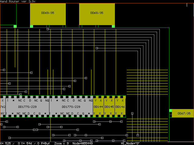
Figure 1. KDPV
What prevents such grandees of training of domestic microelectronics, such as, for example, MEPI and MIET, to do the same as their foreign colleagues (for example, MIT or UZH), namely, to enable graduate students to produce their own crystals? You can, of course, assume that the release of your own crystal is extremely long, complex and expensive, and therefore expensive for an institute, and unbearable for a student. However, it is not. Let's take a look at one of the available technologies in the domestic microelectronics market, familiarity with which will allow the student to become much more attractive in terms of future employment, and the offer of which for the student will allow the university to significantly raise its rating in the eyes of applicants and employers.
2. What is BMK?
BMK is a basic matrix crystal. Not become clearer? Then we will take a step aside and look at the highly simplified production cycle of a customized chip (ASIC):
- Development of schema description
- Topology creation
- Transferring process files to the plant and waiting for crystal availability
- Measurements of the crystals obtained
- Enclosure
- Sale
There are two very "long" points here - the development of a scheme and the expectation of the results of the plant’s work. To reduce development time, various methodologies are applied, and in the student environment the best solution is teamwork, but we are interested in the second point — the plant operation time. Due to the fact that the microelectronic plant is a very inert production, everything should be as planned. Did not have time to start the production? Next try in a quarter. The production itself, depending on the complexity of the product, can last up to six months. Moreover, these six months is an approved production cycle on highly automated machines, and not the carelessness of the staff. How can you reduce these periods? By making a common basis in all the schemes produced, so that the stage of making differences is fast.
This common basis is the BMC - a crystal with pre-arranged transistors, the functional purpose of which is determined by the metallization layers, which allow interconnecting transistors. These interconnects form the unique functionality of the crystal.

Figure 2. Hand Router v3.3, originally from NICEVT, was created in the 1980s – 1990s.
At one BMK, using different metallization schemes, it is possible to produce hundreds of different microcircuits for various organizations. For the plant, in this case, BMK itself becomes a mass-produced serial product, and the finishing stages, ie the metallization layers, can be quickly changed according to customer requirements. Thus, we get more frequent “launches” of new products into production and lower prices. For student development, both of these items are extremely relevant.
3. Why precisely BMK?
Let's compare the benefits of using different teaching methods and see what gives the greatest effect at the lowest cost.
Table 1. Comparison of the educational effect of learning using various techniques
Header encoding, because otherwise it does not fit in the width of the layout.
A - FPGA-oriented design
B - BMK without the use of FPGAs and with real release
C - BMK using FPGA and with real release
D - ASIC without the use of FPGAs and without real release
E - ASIC with FPGA and without real release
F - ASIC with FPGA and real release
G - The current training program in MEPI, Department. 27
| Route component | A | B | C | D | E | F | G |
|---|---|---|---|---|---|---|---|
| Formulation of the problem | ■ | ■ | ■ | ■ | ■ | ■ | ■ |
| RTL programming | ■ | ■ | ■ | ■ | ■ | ■ | ■ |
| ASIC-oriented RTL programming | □ | ■ | ■ | ■ | ■ | ■ | □ |
| Work with modern CAD | ○ | ■ | ■ | ■ | ■ | ■ | ○ |
| Understanding the FPGA-Specific Code | ■ | □ | ■ | □ | ■ | ■ | ○ |
| Understanding synthesizer performance | □ | ■ | ■ | ■ | ■ | ■ | ○ |
| Understanding Constrain Requirements | ○ | ■ | ■ | □ | □ | ■ | □ |
| Understanding the importance of placement and tracing | ○ | ■ | ■ | □ | □ | ■ | □ |
| Testing | ■ | ■ | ■ | ■ | ■ | ■ | □ |
| Creation of verification environment | ■ | ■ | ■ | □ | ■ | ■ | □ |
| Multi-corner modeling | ■ | ■ | ■ | ■ | ■ | ■ | □ |
| Simulation with extraction | □ | ■ | ■ | ■ | ■ | ■ | □ |
| Enclosure | □ | ■ | ■ | □ | □ | ■ | □ |
| Analog circuitry | □ | ■ | ■ | ■ | ■ | ■ | ○ |
| Work with measuring installations | □ | ■ | ■ | □ | □ | ■ | ○ |
| Work in the laboratory | ■ | ■ | ■ | □ | □ | ■ | ○ |
| Cost of | one | 2 | 3 | 0 | one | four | 0 |
■ - is present in the program;
□ is not in the program;
○ - possible options.
This table is filled exclusively from my vision of how the presence of a particular stage in a certain spherical graduation project in a vacuum affects the performance of students. In reality, someone can master the entire route without teaching help, while others are unable to write a multiplexer on Verilog. The string "cost" reflects the positioning in the top, but by no means multipliers. Also, the "cost" does not take into account the actual cost of CAD, for a number of different reasons.
Now it becomes clear that with less additional cost, the route aimed at the release of the BMC, with the use of FPGAs and with real release, covers exactly the same set of skills that is necessary for the release of ASIC. The remaining routes, although nominally, cover a large range of skills, in practice, in good faith, students are not executed due to the lack of motivation to exert a lot of effort without any visible result.
4. Market Overview
Today, the design of entry-level microchips has become quite a simple task: everyone has heard about FPGAs (programmable logic integrated circuits), circuit synthesizers from code, component placement programs, and subsequent trace circuits. At the same time, many novice developers can hardly imagine what a BMC is, how to work with it, and what advantages it gives. Unfortunately, manufacturers of BMC, this situation leads to the following results:
“The analysis of 2009 shows the outflow of a part of consumers due to the expansion of the field of application of imported FPGAs on the basis of issued permits.” (C) Anstrem OJSC annual report for 2009.
In today's microelectronics market there are many manufacturers of BMC: both domestic and foreign. In particular, in the Union State of Russia and Belarus there are at least six manufacturers of microcircuits that offer their own BMC for development: Angstrem OJSC, IEC NN, Progress Scientific Research Institute of Awareness, Technological Center NPK, Physics Research and Production Corporation and Minsk Integral ".
Usually, specialized CAD systems from well-known companies, such as Cadence, Synopsis or Mentor Graphics, are used for the development of microchips; however, in the case of BMK, everything is somewhat more complicated. Official support for BMK, as a separate type of chip, this software does not provide, but it is possible to make it work in the right mode with the help of various tweaks. In this situation, BMK developers have to develop their own unique design routes, which are sometimes used along with independently developed software by OpenSource software, for example, Yosis.
- In the case of Angstrom, finding the exact information used by the CAD system is very difficult. There are, however, prerequisites to assume that their CAD "Nevod" is no longer used and the transition to the use of Cadence products has been made.
- IEC NN, OAO NPO Fizika, AO NIIMA Progress and Integral, do not provide information on the CAD system used, however, the PDK Integral under Cadence, so it can be concluded that the rest of the route is also there.
- NPK "Technological Center" use their CAD "Ark", which implements almost the complete design route. In any case, this is stated on their website.
5. How many gates are enough for everyone?
A popular reason for the reluctance to work with BMK is uncertainty about whether the scheme being developed will “fit” into this BMK and at what speed it will all work. Of course, it’s good when there is a BMK series with a single design library, and you can jump to a larger or faster crystal if necessary, but this is not always possible. Here, for example, everything is clear about TSMC: there are many companies that openly declare the speed of their schemes performed on one or another of those. process. And what about our BMK? Where generally to take a list of products created on the basis of BMK, and see their performance?
A few examples:
- Digital-analog BMK. About 300 gates + 8 power transistors. Implemented a timer circuit for 2 minutes with two levels of protection. Load control on current mirrors, power transistors for load control. Reduced power consumption, work with quartz 32.768 kHz, supply voltage range from 1.8V to 9V.
- Digital happy. resistant BMK. 100,000 gates. Logic specials destination + NCO (numerically controlled oscillator). Battery phase 40 discharges, sine - 12 discharges. Two registers control the sine frequency, parallel and sequential control. The output is parallel.
- Digital-analog BMK. About 400 gates + DAC 10 bits. Sinus generator for 7 digits with current output.
- Digital BMK. From 1500 to 3000 valves. Various terminals multiplex channel GOST 26765.52-87.
- Digital BMK. About 500 valves. Eight-channel generator to control the primary windings of transformers.
- Digital BMK. About 3000 valves. Majority scheme for 8-bit bus.
Unfortunately, the specificity of the market leads to the fact that the vast majority of developments at BMK remain unknown to the general public. Public data does not give a clear idea of speed, and the figures stated in the brochures look ambiguous. At the same time, it’s not much to get familiar with technology for the tasks, and already having some experience behind it is much easier to give a rough estimate of the complexity of a particular circuit.
6. The development process
We turn to the most interesting. We have: BMK for ~ 3k valves (1 valve = 2 CMOS transistors) with channel architecture, wiring in one layer of metal and polysilicon sublayer; enthusiasm; approval of the management of the company for self-study employee.
The idea of the future crystal was born out of idleness, namely, from reading one forum, where, in particular, there was a conversation about circuit design compact solutions for calculating sine codes. I found this topic interesting, and I decided to see what can be done in this area.
Now let's see what was done, what was not, what mistakes and what conclusions were made.
6.1 Design
Surface studies have shown that there is an algorithm for calculating the values of sine, which of mathematical operations requires only summation, subtraction and shift to the right. It turned out that this is not just an algorithm, but a whole family called CORDIC (Coordinate Rotation Digital Computer). Those interested in the details of the algorithm can refer to the bibliography at the end of the article, and I will just clarify that using this algorithm you can calculate not only the sine, but also the cosine, arctangent, multiply and divide the arguments, and consider some hyperbolic functions.
Having studied a lot of publications on this algorithm, and having systematized this knowledge in my head, I figured out that you can try this algorithm at a BMK with a capacity of about 3k gates.
So, what we have in the end on the architecture of the scheme?
- Expanded pipelined CORDIC algorithm for calculating sine.
- 4 additional digits in internal data buses to compensate for rounding errors.
- 11 bit accumulator adder for phase value.
- The phase increment is set by the parallel bus.
- Output data format: 7 digits + sign, parallel bus.
Everything seems to be fine, but what will happen if you do not compensate for rounding errors? Here's what (comparing the internal bus 11bit and 8bit):
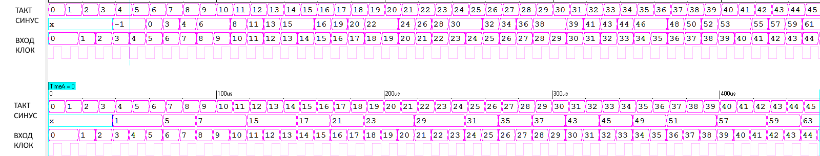
Figure 3. Comparison of the output of the CORDIC algorithm with the use of 11bit and 8bit internal buses, respectively.
If you look at the second lines of data, you can see that rounding errors can effectively lower the quality of your calculations.
If we later attach this chip to the DAC for 7 bits, then we get a perfectly usable sine generator (DDS, in our opinion, direct digital synthesis). In this case, we will have the opportunity for frequency modulation of the sine, but there will be no possibility for phase modulation.
In general, the route of working with small BMK is somewhat different from the design route that is now generally accepted. If you think about it, the differences become obvious: with such a small valve volume, it is necessary to use each valve extremely efficiently, and the main paradigm of modern design is not at all that. She says that the product must be architecturally compatible with modern systems of automated testing, verification, measurement at every stage. At the same time, the question of valve efficiency remains outside the brackets, as the necessary overhead costs. Indeed, in the years of dynamic development of production technologies, thinking about efficiency was superfluous. That's when (and if) we still reach the physical limit and stop increasing the density of transistors on a chip, then the issues of efficient use of space will face us in full growth. Well, with small bmc they already stand up to their full height, and therefore the conclusion is that at small bmc of small containers, you can and should use complex designs using various clever schemes for generating clocks, various latches, feedbacks and other things for which you use in the modern route senior engineer hands would pootryvat.
The main problem of using such things is that in order to use them the engineer must clearly be aware of what he is doing and why. However, if there is an understanding, then the gain can be fantastic. If there is no understanding ... well, you can shoot in the foot in a million different spectacular ways.
What did the design route look like in my case:
- Manual drawing of the scheme in the form of the scheme from library elements
- Estimation of the resulting volume of the scheme
- Processing the scheme until the volume of the scheme exceeds 80% of the capacity of the BMC
- This also includes work on creating new library elements, testing them and integrating them into the design route.
- Making tests for the scheme
- Manual tracing scheme
Experienced designers here may immediately argue that several important stages have been missed, but I really did not forget to mention anything.
Manual design shows very well how important a high-quality component library is. The first versions of the circuit did not fit into the crystal simply by the volume of logic, and in fact, in the case of a channel BMK — one where the wiring goes through the channels laid between the “lines” of transistors — about 30% of the circuit's volume is occupied by interconnects. Therefore, we had to expand the library somewhat, based on the topology that was obtained in this particular project. This approach allowed to save a significant number of valves and even more or less freely lay all the tracks.
The final filling of the crystal - 72%, another third of the crystal went to the layout. Then the files were transferred to the plant, and I returned to my current working projects.
When using the “manual” design method, the following points should be kept in mind:
- You can not mindlessly use library elements, based on their function. It is necessary to study what this element is made of at the transistor level, whether it is digital or analog. What is its load capacity for inputs and outputs, whether it is pure CMOS logic, or TG, or something else.
- It is necessary to take into account and coordinate the power elements and their load.
- If you have a synchronous trigger, then you need to clock it with signals of equal power.
- If you use some kind of signal without intermediate amplification, and it is loaded on many consumers, then the signal can fall too much. This may be insignificant in normal conditions, but is critical when testing for WWF (external factors).
No simulation system will replace your own brains. In general, you can not run the simulation, if you do not understand how the circuit works.
6.2 Measurements
An extremely important stage in working with a crystal is its measurements. Three types of measurements can be distinguished: technological, functional, electrical. The first check that the plant is not nakosyachil and the crystal is technologically correctly made. The latter verify that the theory (i.e., modeling) converges with practice (real crystal). Still others are responsible for such parameters as: consumption currents, leakage currents, input and output currents, etc. Here it is extremely important to understand that measurements on a real probe device are not at all the same thing as simulation. And this is not even the same as the work of the enclosed chip on the board as part of some device. Often, it is much worse in terms of the working conditions of the crystal. After all, the probe apparatus is one thing, and the measuring system is another. There is a loop between it, interconnects ... And this is all nothing but a huge number of parasitic resistors, capacitors and inductances. Therefore, tests for the measuring installation are created separately, taking into account the physics of the processes.
And measuring installations are different, and each of them has its own characteristics and nuances. For example, the Fairchild installation comes from the 80s of the last century, the interface is not USB, but a tape cassette. In the domestic installation FORMULA, after the first recorded error, in the time diagram of the measurement, randomly still some "phantoms" appear that easily disappear after fixing the first error. Measuring from HP lives on some ancient Unix and communicates with the outside world exclusively over the network. In National Instruments measurement, the position of the strobe is set not in the same way as in all, but in its own special way, which imposes its own restrictions on the formation of test sequences (vectors). There are still measuring installations from Agilent, with their own nuances. In general, the idea is clear, yes?) It will not be easy and simple.
And the student, in an amicable way, would have to work with each of the measuring installations in order to have a broad understanding of this process. Because life is more difficult than our expectations, and the fact that initially the crystal was measured at, say, Fairchild, does not mean that the following measurements will not have to be carried out at NI. Thus, there must be some initial set of tests that is applicable to each of the measuring systems in use by means of various kinds of software converters. If something is not taken into account when drawing up the tests, it may be impossible to use any measuring system, or the consistency of these test vectors with each other will be broken.
In general, for beginners, I have a small list of rules and reminders that must be followed when taking measurements:
- If there are no good reasons for this, then the measuring system should be considered as obviously working.
- The probe machine must be properly in contact with the plate. If there is no contact, then it makes no sense to carry out further work.
- The "fast" test may not work properly when measured with a snap with long wires.
- The test itself can be illogically composed, without taking into account the physics of the processes underway, such as non-synchronism of the general reset signal, for example.
- Plates can be different in quality.
- The crystals on the plates may contain various defects:
- Topological
- Circuitry
- Technological
- All inputs / outputs, other than purely digital, must have their estimated current consumption. The current consumption of the chip should be calculated taking into account all the inputs / outputs.
- It should be remembered about the values of voltages and currents established for different drivers of the measuring system.
- Circuit error during measurement can be considered found if it is regular. That is, it is repeated independently of the plate and the crystal on the plate.
- If the error is not critical, then it must be "taken into account" in the source files and re-write tests so as to eliminate it.
- If you make changes to the source files after the release of zero crystal correction, then you should always keep a history of changes.
The list can be expanded further, but it gives a good idea of what nuances can emerge upon first acquaintance with the process of measuring a crystal.
But now let's move on to practice. After only 4 (!) Weeks , plates with ready-made crystals were obtained. Plate measurements have shown that the circuit works, but not entirely. Remember about the shot in the leg, right?) I successfully shot myself in the foot ignoring the above-mentioned item “Extraction of parasitic parameters from the topology and re-modeling” at the design stage.

Figure 4. Meme.
But there is nothing to do, it is necessary to study what and why it does not work. A pre-prepared layout is not suitable, and therefore we take a universal breadboard, a soldering iron and go ahead. After 80 wires, one arduin, a couple of cases of universal logic and several liters of coffee, a working model was obtained, which not just flashed a light bulb, but played me an 8-bit lambad.
Well, more seriously, then a couple of waveforms. At different clock frequencies and different predetermined phase increments per clock, the following sinusoids can be obtained:

Figure 5. Large phase increment per cycle

Figure 6. Slow phase increment per clock
That is, the smaller the phase increment per cycle, the smoother the sinusoid is.
However, a negative result is also a result. Conclusions were made, the experience gained. The enthusiasm is warmed up by an 8-bit lambada to unprecedented quantities. Make a second correction.
6.3 Second Chip Correction
What should be done next?
- To recognize the current version of the chip insolvent;
- Explore NCO construction options (numerically controlles oscillator) for more details;
- Find, research, develop a variant of NCO based on the ROM compression technology (cROM);
- Develop a compressed multiplication scheme with sufficient accuracy for a specific task;
- Develop for components library:
- Multiple static memory cell options
- Several options for reading memory amplifiers
- Several options for addressing cells in memory
- Choose from the variety of options the one that should give the best result;
- Optimize applied library elements for a specific project;
- Design BMK

Figure 7. Intermediate version of the crystal topology loaded into HRT.
The final parameters of the released chip:
- Filling BMK - 83%.
- 14 Phase Storage Drive
- Set the increment of the phase 11 bits
- Complementary phase outputs (sin & cos, 12 digits) to parallel buses
- 16 MHz input frequency
Unfortunately, the oscillograms of this version I have not survived, and what else is there to watch? This version works well in the entire specified range of temperatures and voltages, and the result in frequency was even better than expected. Tracing this version of the chip was quite complicated, but the desire to fit the same scheme has won all the difficulties.
The development of this microcircuit for me has always been like a kind of minor project, but at the same time quite fascinating. I got a lot of knowledge about the many different interesting areas of design, which initially was not very, and wanted to dive. If you are a student, and you have the opportunity to release your own firmware for BMK as a graduation project - grasp this opportunity with both hands. This kind of experience is invaluable.
7. And why is this all and how much is all this?
These are very correct questions.
Let's start with the second.
30 000 rubles worth the release of one plate with a diameter of 100mm using 2 micron technology. For this money we get a huge amount of experience that will settle "at the fingertips" of students. Even if in the future this student goes to program the FPGA, he will never have a question about what Setup & Hold is, he will never forget that the Verilog code is not just a program, but an algorithm running on a real device, and external signals - not just digits of a logical state, but a complex chain containing many parasitic elements. Depending on the chosen BMC, one can try out a full-fledged modern digital route, and a hybrid one - migration from FPGA to BMC, and mixed modeling, verification of any difficulty levels, analog circuits ... the scope is limited only by students' imagination. And most importantly - the theoretical training will be supported by its crystal, standing on the shelf and flashing light.
Note. Comments about errors in the article, please send to the PM.
Accepted Abbreviations
Higher education institution
MEPhI Moscow Engineering Physics Institute
MIET Moscow Institute of Electronic Technology
MIT Massachusetts Institute of Technology
UZH Universität Zürich
BMC Base Matrix Crystal
ASIC Application specific integrated circuit
FPGA Programmable logic integrated circuit
CAD CAD software
CMOS Complementary metal oxide semiconductor [technology]
CORDIC Coordinate Rotation Digital Computer
-
NCO Numerically controlled oscillator
ROM Read-only memory
cROM Compressed ROM
Literature
- CORDIC IP Block Design, Vitaliy Kuhar, Stockholm, Sweden 2008
- CORDIC. , . . , . .
- Comparison of parallel and pipelined CORDIC algorithm using RCA and CSA, Guerrero, Meloni
- CORDIC for dummies.pdf
- Sine/Cosine using CORDIC Algorithm, Prof. Kris Gaj
- Lecture_cordic.pdf
')
Source: https://habr.com/ru/post/418759/
All Articles